Article

Analytical Study of the Electrical Output Characteristics of c-Si Solar Cells by Cut and Shading Phenomena

Photovoltaics Laboratory, New and Renewable Energy Institute, Korea Institute of Energy Research, Daejeon 34129, Korea
*
Author to whom correspondence should be addressed.
Energies 2018, 11(12), 3397; https://doi.org/10.3390/en11123397
Submission received: 12 September 2018 / Revised: 15 October 2018 / Accepted: 27 November 2018 / Published: 4 December 2018

Abstract

:
Cut solar cells have received considerable attention recently as they can reduce electrical output degradation when the c-Si solar cells (crystalline-silicon solar cells) are shaded. Cut c-Si solar cells have a lower short-circuit current than normal solar cells and the decrease in short-circuit currents is similar to the shading effect of c-Si solar cells. However, the results of this study’s experiment show that the shadow effect of a c-Si solar cell reduces the V o c (open circuit voltage) in the c-Si solar cell but the V o c does not change when the c-Si solar cell is cut because the amount of incident light does not change. In this paper, the limitations of the electrical power analysis of the cut solar cells were identified when only photo current was considered and the analysis of the electric output of the cut c-Si solar cells was interpreted with a method different from that used in previous analyses. Electrical output was measured when the shaded and cut rates of c-Si solar cells were increased from 0% to 25, 50 and 75%, and a new theoretical model was compared with the experimental results using MATLAB.

1. Introduction

The photovoltaics (PV) module is currently being researched to increase electrical output [1]. In terms of methods for improving electrical output, there are studies on increasing the efficiency of c-Si solar cells and reducing the series resistance of solar cells and PV modules [2,3,4].
Cut c-Si solar cells have less resistance because of their small electrical current and area. Therefore, the power output is improved as the FF (fill factor) characteristic is enhanced [5]. The PV module, fabricated by cut c-Si solar cells is receiving much attention even though loss is caused by an increase in leakage current and contact resistance. However, most cut c-Si cell research has a paste and electrode structure and there is a lack of research on the electrical output of cut c-Si solar cells [6,7,8].
Recently, research has been carried out to fabricate PV modules using cut c-Si solar cells. Typical examples are half cut c-Si solar cells and shingled solar cells [9]. Previous research is mainly about reducing contact resistance in the c-Si solar cell or maximizing the area of irradiation that is incident to PV modules. There are no studies on the electrical output characteristics resulting from the division of c-Si solar cells. Cut c-Si solar cells have a smaller area than regular c-Si solar cells, which reduces the I s c (short circuit current) value. In general, the decrease in the current value from cutting the c-Si solar cell is considered the same as the shading effect in c-Si solar cells. Therefore, the I s c value of c-Si solar cells decreases. The crack phenomena, in which parts of a c-Si solar cell are divided, are also considered to have a reduction in the I p h (photo current) value. [10] However, the cut and shading phenomena of solar cells are different. When shaded effects occur, the normal areas of the solar cell are connected to shaded areas, reducing the electrical output of the entire c-Si solar cell [11]. Cutting solar cells is only reducing the overall area of the solar cell, the normal area of the cell is not connected to the shaded area. In other word, the shading effect is the reduction of the photo-generation current by external environmental factors and the cut solar cell does not decrease the photo-generating current but rather the area along the same photo-generation current. Thus, when interpreting the electrical output of a cut solar cell, it is not possible to make a correct interpretation because the voltage values do not match. That is, if the shading effect and cut solar cells reduce the light entering at the same rate, the reduction in the light generation current is the same but the voltage value is not. In this work, the voltage and current were reduced in a shaded solar cell while the cut solar cell only reduced the current and the voltage was the same. Electrical power was compared for the cut and shading phenomena of c-Si solar cells and the limitations of electrical power analysis were reviewed considering only the photo current. In addition, the electrical output in cut c-Si solar cells was analyzed theoretically.
In summary, many PV module companies have produced much of the cutting modules in recent years and cut solar cells are receiving considerable attention. However, it was previously impossible to interpret the exact electrical output of the cut solar cell. The reason was that it was interpreted in the same way as the shading effect of a solar cell. In this paper, the electrical output of the cut solar cell has been analyzed in a way that was not previously possible.

2. Comparison of Electrical Output Characteristics of Cut and Shading Phenomena of c-Si Solar Cells Considering I p h

Because PV modules generate electricity in an external environment, the shading effect can be caused by bird droppings, leaves, and shadows [12,13]. When the shading effect occurs, the current in the c-Si solar cell decreases because no current is generated in the shaded area [14,15]. In addition, cut solar cells reduce the current in the solar cell because no current is generated in that area. The electrons generated inside the c-Si solar cell flow into the finger and electrode (busbar) on the surface of the c-Si solar cell. An electron cannot flow through the finger of a c-Si solar cell because the electrode breaks when the c-Si solar cell is cracked or cut. As shown in Figure 1, a vertical cut of the 3-busbar c-Si solar cell breaks the finger electrode and, therefore, the electrons cannot be collected. Section B is an inactive zone because even if light enters the c-Si solar cell and electron-hole pairs are generated, they cannot flow through the busbar. That is, the c-Si solar cell generates electrical output in area A but not area B.
Figure 2 shows a c-Si solar cell cut horizontally. If the electrode is cut completely horizontally, there is no electrical power at all and there is no need to interpret the electrical output. Therefore, in this study, we excluded c-Si solar cells being cut completely horizontally. That is, c-Si solar cells were cut horizontally but we assumed that the electrodes connected zones A and B. As shown in Figure 2, the electrodes are not shorted, the electrons in the c-Si solar cell can move through the electrodes. Therefore, area B in Figure 2 is not an inactive area, area A and B are connect each other and current flows.
An equivalent circuit considering the output of the normally generated area and cut area of a c-Si solar cell is shown Figure 3. The left side of the center normally generates electricity and the right side is the cut area.
The c-Si solar cell equivalent equation is as follows:
I = I p h I 0 [ e x p q ( V + I R s ) n k t 1 ] V + I R s R s h
where I p h is the photovoltaic current, I o is the saturation current, q is the electron charge, k is the Boltzmann constant, T is the temperature of the PN junction (p-type and n-type Junction), R s and R s h are the series resistance and shunt resistance, respectively, and n is the diode ideality constant. If the c-Si solar cell is cut as shown in Figure 1, the whole area must be removed from the inactive zone. The equation is as follows:
I = ( I p h I p h _ c u t t i n g ) I 0 [ e x p q ( V + I R s ) n k t 1 ] V + I R s R s
where I p h _ c u t t i n g represents the current value of the cut solar cell. In addition, the electrical output of the c-Si solar cell cut horizontally can be interpreted as being connected between A and B. The equation is as follows:
I = ( I p h _ c u t t i n g 1 + I p h _ c u t t i n g 2 ) I 0 [ e x p q ( V + I R s ) n k t 1 ] V + I R s R s
where I p h _ c u t t i n g 1 and I p h _ c u t t i n g 2 represent the current values in areas A and B of the cut solar cell. Since the c-Si solar cell has been cut but has no electrically inactive zone, the I p h may be represented by the following: I p h _ c u t t i n g 1 indicates area A (wide part) of Figure 2 and I p h _ c u t t i n g 2 indicates area B (narrow part). The sum of the areas of the two parts is I p h and is produced by a single c-Si solar cell. The equation is as follows:
I p h = I p h _ c u t t i n g 1 + I p h _ c u t t i n g 2
Because there is no inactive area, the electrical output is the same as a normal c-Si solar cell. The exclusion of inactive areas from the whole light generation current value of the c-Si solar cell in Equation (2) is identical to the shading effect of the c-Si solar cell shown in Figure 4.
In Figure 4, the c-Si solar cell is shaded into an inactive zone in area B, as in Equation (2). The whole photo-generation current of the c-Si solar cell excludes the inactive area.

3. Comparison of Current-Voltage Characteristic by Cut and Shading Effect of a c-Si Solar Cell

3.1. Experimental Method

In this study, we conducted an experiment on the electrical output of the cut and shading phenomena of c-Si solar cells. A single crystalline 3-busbar c-Si solar cell was used for the experiment and the initial output of the c-Si solar cell was measured. Measurements were taken at Chungbuk Technopark Solar Technical Center. The simulator was in the AAA class and the measurement temperature was 25 °C. AAA class means a spectral match at intervals of 0.75–1.25, irradiance spatial non-uniformity of 2% and temporal instability of 2%, according to the American Society for Testing and Materials (ASTM). To ensure that the experiment was accurate, the reference cell current was within the range of the reference value ratio ±0.05 [A] or less and when measuring, we confirmed the temperature change of the c-Si solar cell every 2 minutes. Figure 5 shows a measurement of the current voltage characteristics of a solar cell that is 50% shaded in the vertical direction.

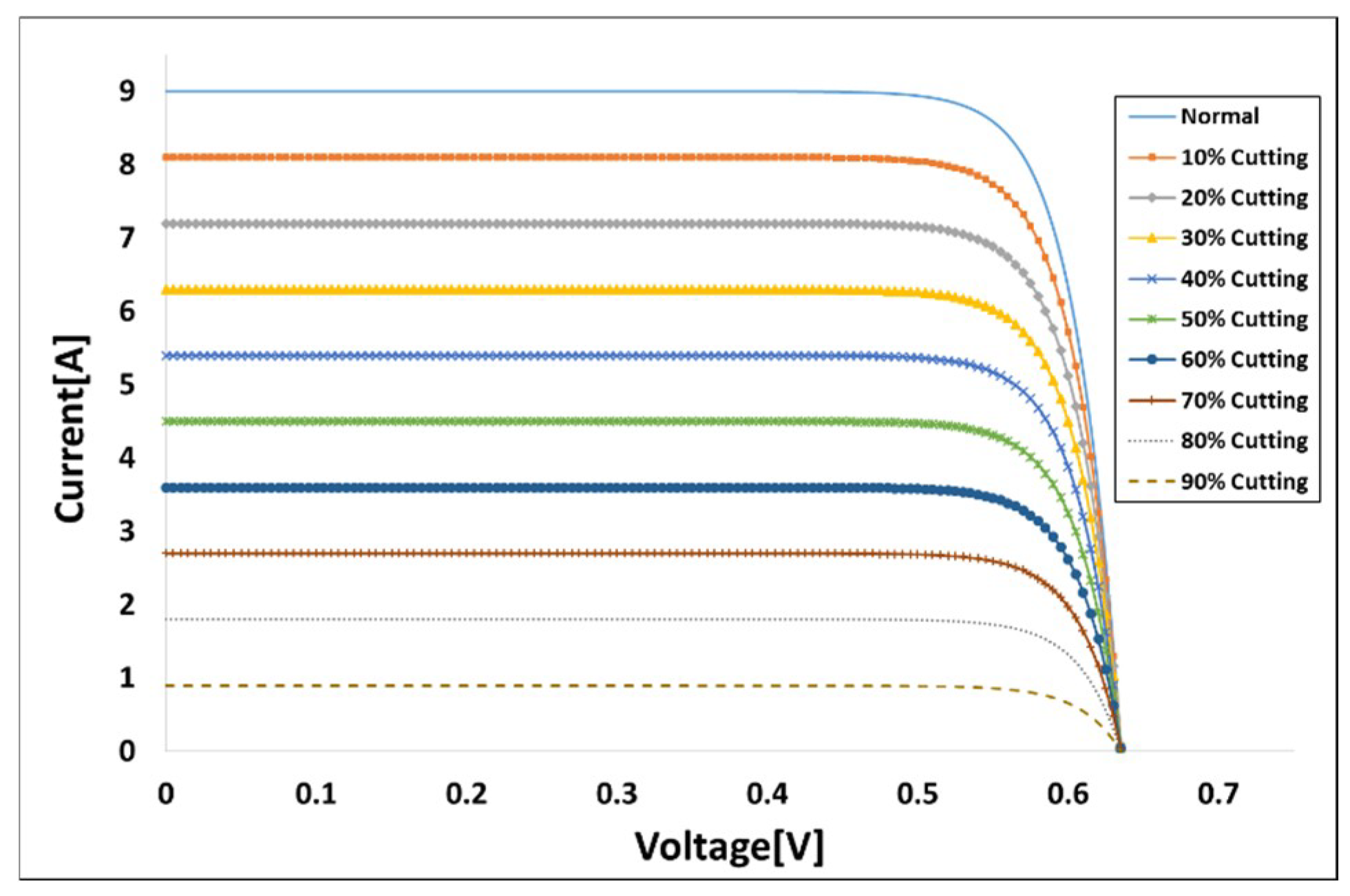
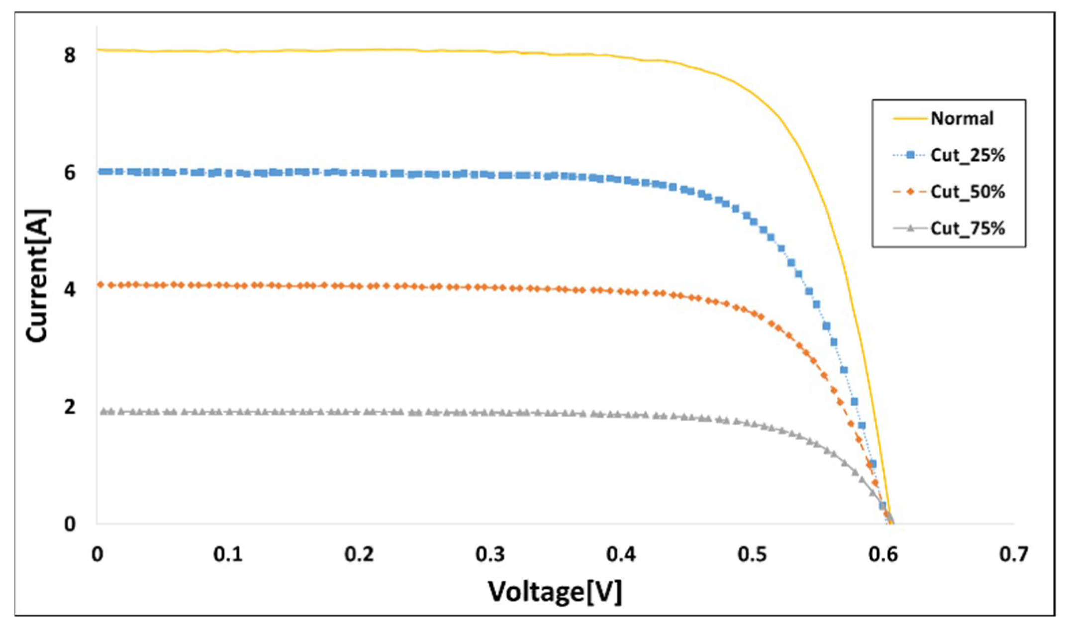
3.2. Results of Electrical Output Experiment for the Cut and Shading Effect c-Si Solar Cells

Before the experiment we measured the initial value of a c-Si solar cell. We then measured the electrical output after the c-Si solar cell was 50% shaded horizontally and vertically. Then, the c-Si solar cell was cut to 50% and the current voltage characteristics were measured.
There was no difference in the horizontally and vertically cut directions of the c-Si solar cell because the electron-hole pairs produced in the PN junctions flowed to the busbar and finger. Figure 6 shows the current-voltage characteristic curve of a c-Si solar cell that is cut horizontally and vertically. Prior to the experiment, two c-Si solar cells with similar initial electrical output were selected, one c-Si solar cell was cut 50% in the horizontal direction and the other 50% in the vertical direction. The current voltage was then measured. The initial electrical output difference between the two c-Si solar cells was as follows: current (A) 0.001, voltage (V) 0.002, and FF (fill factor) 0.09%. The output characteristics were very similar.
The results of the experiment showed that the electrical output of c-Si solar cells cut horizontally were almost identical to those cut vertically. The electrical output of the c-Si solar cell was estimated to be the I p h value caused by the shaded or cut area.
Figure 7 compares the current-voltage characteristics of a c-Si solar cell with respect to the cut and shading effect. The experimental results in the inactive areas caused by the shading and cut phenomena of the c-Si solar cell revealed that the current was equivalently reduced but the V o c value was about 2% different. When a c-Si solar cell experienced the shading effect, there was a change in the voltage value but there was little change in the voltage value for the cut c-Si solar cell. In conclusion, the shading effect of the inactive area of a c-Si solar cell can be interpreted only by considering the light generation current.

3.3. Limitations of the Analysis of Electrical Output Characteristics of a Cut c-Si Solar Cell Considering the Photo-Generation Current

Figure 8 shows the general equivalent circuit of a solar cell. Reducing the I p h value, such as by interpreting the shading effect, results in smaller V o c values as well. Cut c-Si solar cells have the same inactive areas but they do not produce voltage drops in normal areas and, therefore, require a different interpretation. Here, I d is the current flow to the diode, V d is the voltage applied to the diode, R s is the series resistance, and R s h is the parallel resistance.
Figure 9 shows the current voltage characteristic curve according to the value of I p h using a MATLAB (R2016b, Math Works, Massachusetts, USA) simulation program. When the c-Si solar cell is shaded or the irradiation is reduced, as shown in Figure 9, the I p h value decreases and the V o c value decreases slightly.
The semiconductor material composed of PN connections has a depletion layer and a potential barrier, which varies in value depending on the concentration of electrons. In addition, the concentration of electrons depends on the temperature, the forward/reverse bias, and the light intensity. Sunlight has energy and the amount of energy varies with the value of the electron-hole pairs produced in the c-Si solar cell. If the amount of light is reduced, the current and voltage are reduced. The simulation shows that the initial electrical output of a c-Si solar cell without the shading effect is a current (A) of 9 and the voltage (V) is 0.635. The initial value represents the electrical output value of 0% shaded solar cells and Figure 9 shows the current-voltage characteristic curve when the area of the shaded solar cells is increased by 10%. The results of the simulation showed that the current value and voltage value decreased as the shaded area of the shaded solar cell increased.
A c-Si solar cell divided in half and connected in parallel is expressed in Figure 10. Area_1 is the normal operating area of the c-Si solar cell and, assuming Area_2 is inactive, I p h at the normal operating area does not degrade the voltage; there is no reduction in electrical output. However, in shaded areas, voltage drops occur because of the reduction of I p h .
In Area_1 normal current and voltage occur but in Area_2 the voltage drop caused by the shading effect causes the overall output to decrease. This reduced not only the current but also the voltage. However, cut c-Si solar cells produce electrical power in the normal area of Area_1 so there is no voltage drop. In other words, cut c-Si solar cells have the same reduced value of I p h as a shaded c-Si solar cell but do not produce a voltage drop. Thus, the electrical power of a cut c-Si solar cell needs an interpretation different from the shading effect of c-Si solar cells, which takes into account only the value of the I p h .

4. Analysis of Electric Output Characteristics of a Cut c-Si Solar Cell

4.1. Theoretical Analysis of the Electrical Output of a Cut c-Si Solar Cell

When light energy is absorbed into a c-Si solar cell, the electrical current occurs in the PN junction, which is normally expressed as a light-generating current. The carrier generation rate by light is g o p t [ 1 cm 3 s ] , the area is A[ cm 2 ] , the charge amount is q[c], and the light generation current is as follows [16]:
I p h = q A g o p t
When light enters a c-Si solar cell, electron-hole pairs are created. When E p h E g [eV] magnitude of energy enters a c-Si wafer, an electron-hole pair is separated and a current flows through the c-Si solar cell. When light enters a semiconductor, an electromotive force is generated by the light and the optical power density ( P v ) that is generated through the unit area per hour can be expressed as Equation (6).
P v = E p h F v
where α is the absorption coefficient, F v is the number of photons moving at any one point, and E p h is the energy of the photon [16].
When the intensity of the light is higher, the value of the optical power density is greater. Therefore, I o p [ eV / cm 2 s ] , which represents the light intensity, is used as follow [16]:
I o p = E p h F v = P v = h c λ F v
where h is the Planck constant, c is the velocity of light, and λ is the wavelength of light. When light is absorbed into a semiconductor, the amount decreases depending on the depth. This is equivalent to a decrease in the optical photon flux. The variation ratio of the optical photon flow ( F v ) at any one point inside the semiconductor is as follows [16]:
Δ F v ( x ) = F v ( x + d x ) F v ( x )
Δ F v ( x ) = F v ( x ) d x Δ x = 1 E p h d p v ( x ) d x Δ x
As light enters the semiconductor, it changes the optical power density and the variation of the optical power density relative to the distance from the surface is as follows [16]:
Δ P v ( x ) = P v ( x + d x ) P v ( x ) = d P v ( x ) d x Δ x = α P v ( x ) Δ x [ W / cm 2 ]
where α is the light absorption coefficient that determines the optical generation rate of the c-Si solar cell as follows [16]:
Δ F v ( x ) = 1 E p h ( α P v ( x ) Δ x )
Considering energy of a photon, it can be expressed as follows [16]:
Δ F v ( x ) = h c λ ( α P v ( x ) Δ x )
In any one point, the optical power density is P v ( x ) = P v 0 e a x , which can be expressed as follows [16]:
Δ F v ( x ) = h c λ ( α P v ( x ) Δ x ) = h c λ ( α P v 0 e α x )
The carrier generation rate by light can be expressed as follows [16]:
g o p t = Δ F v ( x ) Δ x = α P v ( x ) h v = α P v 0 h v e a x
When the cross section of the solar cell is referred to as A [ cm 2 ] and the light is applied to the PN Junction, the photovoltaic current ( I o p t ) generated by the light is as follows [16]:
I o p t = q A g o p t
In other words, the I p h in the c-Si solar cell is as follows:
I p h = qA α P v 0 h v e a x
Equation (16) is applied to the c-Si solar cell equivalent equation as follows:
I = I p h I 0 ( e x p q V n k t 1 ) = q A α P v 0 h v e a x I 0 ( e x p q V n k t 1 )
The reverse saturation current I 0 is:
I 0 = q A ( L p τ p P n 0 + L n τ n n p 0 )
Therefore, the solar cell equivalent equation is:
I = I p h I 0 ( e x p q V n k t 1 ) = q A α P v 0 h v e a x q A ( L p τ p P n 0 + L n τ n n p 0 ) ( e x p q V n k t 1 ) I s h
where L p is the diffusion length of the hole, L n is the diffusion length of the electron, τ p is the minority carrier lifetime of the hole, τ n is the minority carrier lifetime of the electron, P n 0 is the concentration of the holes on the n-side just near the junction, and n P 0 is the concentration of the electron on the p-side just near the junction, respectively. When a c-Si solar cell is shaded, it reduces only I p h . However, the cut c-Si solar cell also reduces the overall area. Therefore, the I 0 and I sh also should be considered. The equivalent circuit of a c-Si solar cell is shown in Figure 11 when a single c-Si solar cell is divided into many small c-Si solar cells and connected in parallel.
In Figure 11, if each small c-Si solar cell has no electrical losses caused by a connection and each c-Si solar cell has the same electrical characteristics, the following equations apply:
I p h 1 = I p h 2 = I p h 3 = I p h 4 = I p h n
I d 1 = I d 2 = I d 3 = I d 4 = I d n
R s 1 = R s 2 = R s 3 = R s 4 = R s n
Assuming that the light-generation current of a small c-Si solar cell, I p h 1 , I p h 2 , I p h 3 , I p h 4 and I p h n combined, is I p h , the value of the light-generation current of a single solar cell is as follows:
I p h 1 + I p h 2 + I p h 3 + I p h 4 = I p h
The R s h of a solar cell is assumed to be equal in the same c-Si solar cell because it is caused by leakage currents generated by wafer fabrication or process. Since R s is also the series resistance of c-Si solar cells, it was assumed that if the area is the same, the value is the same.
Figure 12 assumes that the red square box is an inactive part of a normal c-Si solar cell.
The total current output of a c-Si solar cell is expressed as follows:
I _ n = J 1 + J 2 + J 3 + J 4 J n
Current in the cut area is as follows:
I _ c = J c 1 + J c 2 + J c 3 + J c 4 + J c n
When the generation current of a c-Si solar cell excludes the current in the cut area from the current of the entire c-Si solar cell, it is as follows:
I = I _ n I _ c
where I represents the current value of a c-Si solar cell after it has been cut and I _ n represents the total current value of a c-Si solar cell. The value of I _ c indicates the current in the inactive part caused by the cut. As the area of the cut c-Si solar cell is part of the total c-Si solar cell area, I _ c can be represented as follows:
I _ c = n = 1 A r e a _ c n = 1 A r e a _ t I _ n
where Area_t indicates the total area of the c-Si solar cell and Area_c denotes the area of the inactive part due to the cut. That is, the entire area of a c-Si solar cell can be represented as the sum of all the small areas, just as the current densities, under Equation (25), are combined. The total area of a cut c-Si solar cell can be expressed by adding all the small areas of a cut.
In addition, Equation (25), which indicates the normal part of the current, may be expressed as follows:
I _ n = 1 n = 1 A r e a _ t I 1 + 1 n = 1 A r e a _ t I 2 1 n = 1 A r e a _ t I 3 1 n = 1 A r e a _ t I 4 + 1 n = 1 A r e a _ t I n
Equation (19) is applied to Equation (29) as follows:
I = q n = 1 A r e a _ t α P v 0 h v e a x q n = 1 A r e a _ t ( L p τ p P n 0 + L n τ n n p 0 ) ( e x p q ( V + I R s ) n k t 1 ) n = 1 A r e a _ t I R s h q n = 1 A r e a _ c α P v 0 h v e a x q n = 1 A r e a _ c ( L p τ p P n 0 + L n τ n n p 0 ) ( e x p q ( V + I R s ) n k t 1 ) n = 1 A r e a _ c I R s h = [ I p h _ n I 0 _ n ( e x p q ( V + I R s ) n k t 1 ) ( V + I R s _ n ) R s h _ n ] n = 1 A r e a _ c n = 1 A r e a _ t [ I p h _ n I 0 _ n ( e x p q ( V + I R s ) n k t 1 ) ( V + I R s _ n ) R s h _ n ]
Equation (30) expresses the current of a c-Si solar cell with the sum of the area of a small part expressed as follows:
I = n = 1 A r e a _ t n = 1 A r e a _ c n = 1 A r e a _ t [ I p h I 0 ( e x p q ( V + I R s ) n k t 1 ) ( V + I R s ) R s h ]
Figure 13 shows the simulation results of Equation (31) in the MATLAB simulation. A cut c-Si solar cell reduces the current values only because the generation area gradually decreases with the size of the inactive area. The simulation shows that the initial electrical output of a c-Si solar cell without the cut ratio has a current of 9 and a voltage of 0.635. In Figure 9, the voltage value as well as the current value is reduced according to the shading ratio, but only the current value is reduced as a result of Figure 10. This means that the electrical output of a solar cell can be interpreted by Equation (31).

4.2. Experimental and Simulation Results

In Equation (31), of a cut c-Si solar cell, only the current value changes. The voltage value does not change. This is shown in Figure 13. In order to compare the difference between the shading effect and the electrical output of a cut c-Si solar cell, the experiment was conducted at a proportion of the same area. The electrical output experiment for the shading effect and cut were performed at 0, 25, 50 and 75% of the total c-Si solar cell area and, as in previous experiments, solar cells with almost the same initial electrical output were used. Figure 14 shows a solar cell cut at a ratio of 0, 25, 50 and 75%.
Figure 15 and Figure 16 show the results of our experiment on the current-voltage characteristics of c-Si solar cells according to the shading effect and cut rates.
As in previous experiments, the current and voltage values decreased when the shaded area increased. However, as the cut area increased, the voltage value of the cut c-Si solar cell was almost the same, although the current value greatly decreased. When partially shading effects occur on a c-Si solar cell, there are areas of normal generation and areas where voltage is degraded by shadows, thereby reducing the overall voltage. However, the characteristics of the voltage do not change because the cut c-Si solar cell changes the whole area and not the I p h . As a result of our experiment, we found that the difference between the shading effect and the cut of the c-Si solar cell cause changes only to the voltage value.
Figure 17 shows the current-voltage characteristic curve in comparison with the theoretical and experimental results of a cut c-Si solar cell. The results of the experiment and the developed mathematical model were very similar, with a difference of about 1%. The experimental and simulation results show that the cut c-Si solar cells experienced a reduction in current values in proportion to the reduction of the area and that the voltage value was unchanged.

5. Conclusions

In this paper, electrical power characteristics are analyzed for cut c-Si solar cells. First, the cut c-Si solar cell’s electrical power was interpreted as a reduction in light generation current. This was the same as the shading effect and was not an acceptable result for analyzing the electrical power of the cut c-Si solar cell. The reason for this is that a shaded c-Si solar cell has a normally generated area and shaded area, which changes the voltage value. However, cut c-Si solar cells cannot be interpreted in the previous way because they only reduce the area in normal areas.
Therefore, in this paper, we proposed a new model considering the area of the light-generated current and the saturated current parts differently from the previous equation that was used to interpret the electrical power characteristics of cut c-Si solar cells. The results of the experiment and the newly proposed model had similar results.
The model proposed in this paper is expected to be used to study the electrical power characteristics of the half c-Si solar cell or shingled c-Si solar cell, which is currently receiving considerable attention.

Author Contributions

J.R.L. wrote the main part of the paper, in particular, the theoretical interpretation and the analysis of the experiment. W.G.S. established the research direction of the paper and suggested a method for conducting the experiment. S.W.K. analyzed the data using the paper and provided important comments. Y.C.J. and H.M. Hwang provided technical ideas and assistance in establishing the experiment. G.H.K. reviewed and revised the overall contents of the paper.

Funding

This research received no external funding.

Acknowledgments

This work was supported by a grant from the Standardization Certification of Korea Energy Agency (KEA) and the Renewable Energy of Korea Institute of Energy Technology Evaluation and Planning (KETEP) funded by the Ministry of Trade, Industry and Energy, Republic of Korea (Project No.71000106, 20163020010890, 20163010012230).

Conflicts of Interest

The authors declare no conflicts of interest.

Nomenclature:

V o c open circuit voltageFFFill Factor (%)
I s c short circuit currentndiode ideality constant
I p h photo current I d current flowing to the diode
I o saturation current V d voltage applied to the diode
R s series resistance g o p t carrier generation rate by light
R s h shunt resistance P v optical power density
I p h _ c u t t i n g current value of the cut solar cell F v number of photons moving at one point
αabsorption coefficient I o p t photovoltaic current
h Planck constant L n diffusion length of electron
E p h energy of the photon τ p minority carrier lifetime of hole
λ wavelength of light τ n minority carrier lifetime of electron
L p diffusion length of hole n P 0 concentration of electron on p-side
qelectron charge P n 0 concentration of holes on n-side
kBoltzmann constant I _ n total current value of a c-Si solar cell
Ttemperature I _ c cut c-Si solar cell is part of the total c-Si solar cell

References

  1. Hajighorbani, S.; Radzi, M.A.M.; Ab Kadir, M.Z.A.; Shafie, S.; Khanaki, R.; Maghami, M.R. Dual search maximum power point (dsmpp) algorithm based on mathematical analysis under shaded conditions. Energies 2015, 8, 12116–12146. [Google Scholar] [CrossRef]
  2. Pei, Y.; Guo, J.; Kou, D.; Zhou, W.; Zhou, Z.; Tian, Q.; Meng, Y.; Wu, S. Precise-tuning the In content to achieve high fill factor in hybrid buffer structured Cu2ZnSn (S, Se) 4 solar cells. Sol. Energy 2017, 148, 157–163. [Google Scholar] [CrossRef]
  3. Isabella, O.; Vismara, R.; Linssen, D.N.P.; Wang, K.X.; Fan, S.; Zeman, M. Advanced light trapping scheme in decoupled front and rear textured thin-film silicon solar cells. Sol. Energy 2018, 162, 344–356. [Google Scholar] [CrossRef]
  4. Poursafar, J.; Bashirpour, M.; Kolahdouz, M.; Vakilipour Takaloo, A.; Masnadi-Shirazi, M.; Asl-Soleimani, E. Ultrathin solar cells with Ag meta-material nanostructure for light absorption enhancement. Sol. Energy 2018, 166, 98–102. [Google Scholar] [CrossRef]
  5. Tada, H.Y.; Carter, J.R., Jr.; Anspaugh, B.E.; Downing, R.G. Solar Cell Radiation Handbook; NASA: Washington, DC, USA, 1982.
  6. Halavani, Z.; Lang, J.F.; Summhammer, J. Results of pressure-only cell interconnections in high voltage PV-Modules. In Proceedings of the 29th European Photovoltaic Solar Energy Conference and Exhibition, Amsterdam, The Netherlands, 22–26 September 2014; pp. 64–68. [Google Scholar]
  7. Summhammer, J.; Halavani, Z. Cell interconnection without glueing or soldering for crystalline Si photovoltaic modules. EPJ Photovolt. 2016, 7, 75401. [Google Scholar] [CrossRef] [Green Version]
  8. Summhammer, J.; Halavani, Z. High-voltage PVmodules with crystalline silicone solar cells. In Proceedings of the 28th European Photovoltaic Solar Energy Conference and Exhibition, Villepinte, France, 30 September–4 October 2013; pp. 3119–3122. [Google Scholar]
  9. Zhao, J.; Wang, A.; Abbaspour-Sani, E.; Yun, F.; Green, M.A. Improved efficiency silicon solar cell module. IEEE Electron Device Lett. 1997, 18, 48–50. [Google Scholar] [CrossRef]
  10. Song, Y.-H.; Kang, G.-H.; Yu, G.-J.; Ahn, H.-G.; Han, D.-Y. A Study on the Electrical Characteristics of Photovoltaic Module Depending on Micro-Crack Patterns of Crystalline Silicon Solar Cell. Trans. Korean Inst. Electr. Eng. 2012, 61, 407–412. [Google Scholar] [CrossRef] [Green Version]
  11. Anurag, S.Y.; Mukherjee, V. Line losses reduction techniques in puzzled PV array configuration under different shading conditions. Sol. Energy 2018, 171, 774–783. [Google Scholar]
  12. Seyedmahmoudian, M.; Mekhilef, S.; Rahmani, R.; Yusof, R.; Renani, E.T. Analytical modeling of partially shaded photovoltaic systems. Energies 2013, 6, 128–144. [Google Scholar]
  13. Bingöl, O.; Özkaya, B. Analysis and comparison of different PV array configurations under partial shading conditions. Sol. Energy 2018, 160, 336–343. [Google Scholar] [CrossRef]
  14. Horoufiany, M.; Ghandehari, R. Optimization of the Sudoku based reconfiguration technique for PV arrays power enhancement under mutual shading conditions. Sol. Energy 2018, 159, 1037–1046. [Google Scholar] [CrossRef]
  15. Jung, T.H.; Ko, J.W.; Kang, G.H.; Ahn, H.K. Output characteristics of PV module considering partially reverse biased conditions. Sol. Energy 2013, 92, 214–220. [Google Scholar] [CrossRef]
  16. Kim, D.M. Microelectronic Semiconductor Physics and Devices, 2nd ed.; Hanbit Media: Seoul, Korea, 2011; pp. 948–977. [Google Scholar]
Figure 1. Vertical cut of a c-Si solar cell.
Energies 11 03397 g001
Figure 2. Horizontal cut of a c-Si solar cell.
Energies 11 03397 g002
Figure 3. Equivalent circuit of a c-Si solar cell with cut or shading.
Energies 11 03397 g003
Figure 4. Vertical shading of a c-Si solar cell.
Energies 11 03397 g004
Figure 5. Actual IV measurement of a c-Si solar cell.
Energies 11 03397 g005
Figure 6. Current-voltage characteristic curve for a 50% vertically and 50% horizontally cut c-Si solar cell.
Energies 11 03397 g006
Figure 7. Current-voltage characteristic curve with 50% cut and shading.
Energies 11 03397 g007
Figure 8. Solar cell equivalent circuit.
Energies 11 03397 g008
Figure 9. Current-voltage characteristic curve according to light intensity.
Energies 11 03397 g009
Figure 10. Equivalent circuit of a c-Si solar cell with 50% shading.
Energies 11 03397 g010
Figure 11. Equivalent circuit of small c-Si solar cells connected in parallel.
Energies 11 03397 g011
Figure 12. Equivalent circuit of small c-Si solar cells connected in parallel when being cut.
Energies 11 03397 g012
Figure 13. Current-voltage characteristic curve according to the cut area.
Energies 11 03397 g013
Figure 14. Cut c-Si solar cell.
Energies 11 03397 g014
Figure 15. Current-voltage characteristic curve according to the shading ratio.
Energies 11 03397 g015
Figure 16. Current-voltage characteristic curve according to the cut ratio.
Energies 11 03397 g016
Figure 17. Current-voltage characteristic curve in experimental and simulation results for a cut c-Si solar cell.
Energies 11 03397 g017

