Article

Analysis and Design of an Air-Coupled DC Transformer with a Hybrid Modulation Control Method

1
Division of Electronic and Informatics, Gunma University, Kiryu 376-8515, Japan
2
Department of Electrical Engineering, Yangzhou University, N. 196 Huayang West Road, Yangzhou 225-000, China
*
Author to whom correspondence should be addressed.
Current address: Tenjin Cho 3-15-38, Kiryu, Gunma, Japan.
These authors contributed equally to this work.
Energies 2019, 12(13), 2570; https://doi.org/10.3390/en12132570
Submission received: 12 June 2019 / Revised: 1 July 2019 / Accepted: 1 July 2019 / Published: 3 July 2019

Abstract

:
DC micro-grid is gaining increasing attention recently due to its highly efficient energy utilization and flexible energy exchange capabilities. In this paper, an air-coupled DC–DC transformer is proposed for the interconnection between the active load and the DC microgrid. The generic problems in an air-coupled power transfer system without ferromagnetic structure are discussed. A bidirectional half-bridge topology is also proposed to suit the characteristics of the stationary load and to realize the bidirectional power transfer between the active DC load and the DC grid. A Hybrid Modulation Method (HMM) is proposed; the small signal model is derived and linear control techniques are applied to the forward power transfer control, and phase model control is applied to the reverse power transfer model. The open-loop system is simulated by PSIM to get the characteristics of the forward and reverse transfer model, and the closed system is built in the MATLAB/SIMULINK to verify the effect of the forward frequency control method and the reverse phase control method. The prototype is built with a dsPIC controller, tests are performed to evaluate the characteristics of the transformer and the power flow control of the bidirectional power transfer.

1. Introduction

With the rapid development of new energy and distributed power generation technology, the DC micro-grid is gaining more and more attention due to its capability of island operation as well as power flow interaction with the utility grid. Protection and contingency management of a DC system has been troublesome and costly due to the non-cross-over feature of the DC system [1,2,3,4,5]. Wireless power transfer (WPT) technology provides a feasible way for isolated protection [6,7,8,9,10,11,12]. The idea behind this technology is to convert electric power into spatial magnetic power, which can be coupled to the load via different means [13,14,15,16,17,18]. The known three major means to implement WPT are the inductive power transfer, resonant power transfer and radiational power transfer [19,20,21,22,23,24,25].
As more loads and storages are integrated into the DC micro-grid, there are increasing demands for the enhanced plug-and-play and bi-directional power flow capability. Therefore, a power processing device that behaves like a DC transformer (DCX) is highly desirable [26,27,28,29].
Based on the aforementioned demand, this paper proposes an air-coupled DC transformer for the active load for the DC micro-grid using wireless power transfer technology. The dual half-bridge topology is proposed. The circuit operation and the small signal model for bidirectional power transfer are analyzed in detail. The hybrid modulation method is proposed which suits the characteristics of each power transfer direction. The proposed DCX is finally verified experimentally with a dedicated prototype.

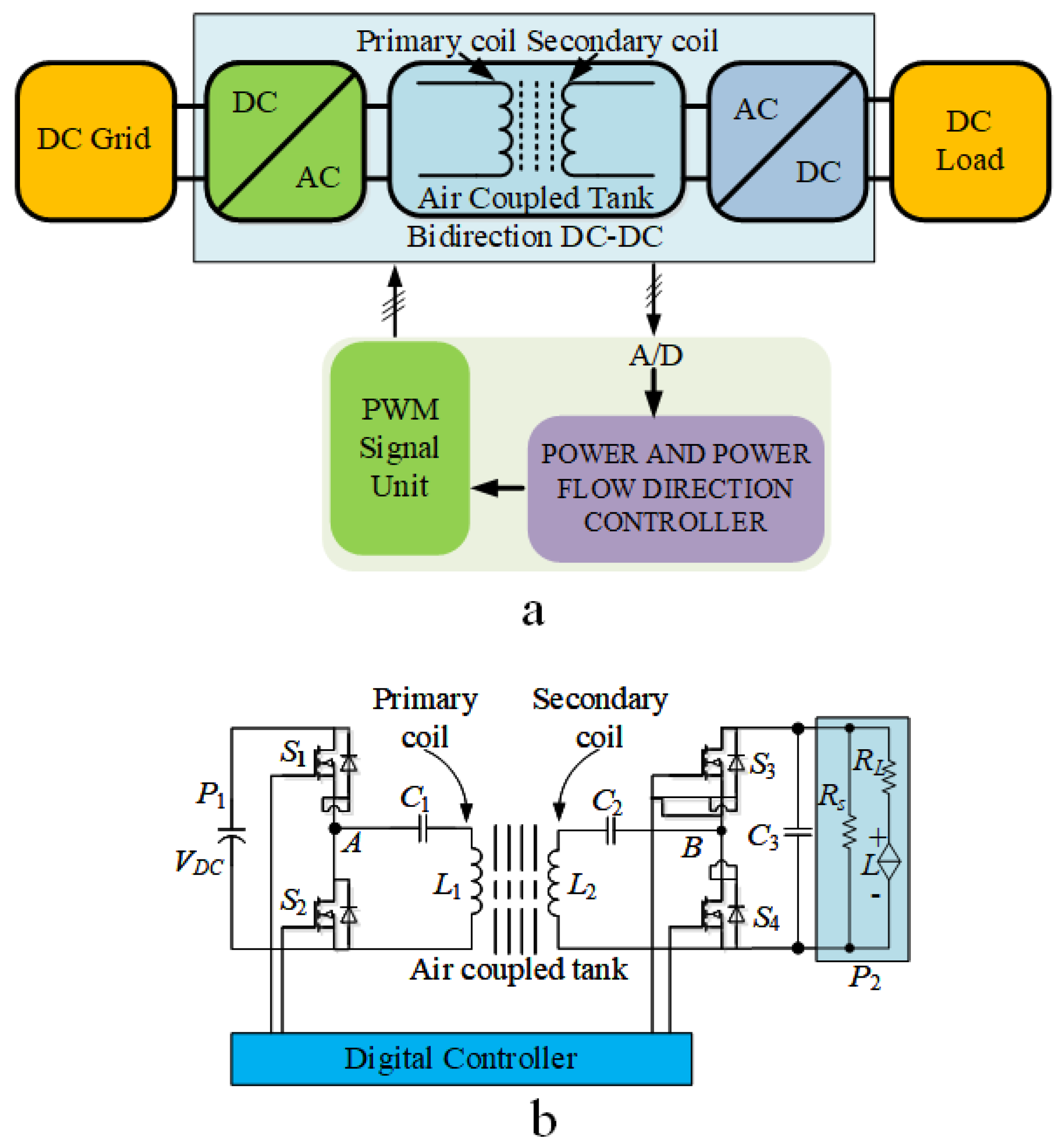
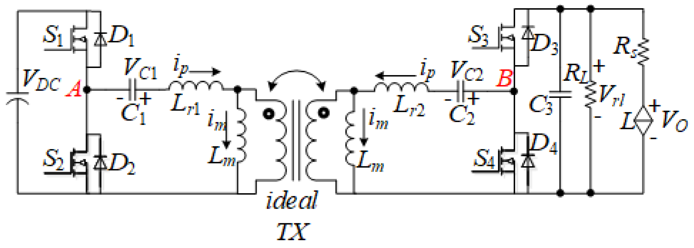
2. Proposed Air-Coupled DC Transformer

Different loads exist in the DC micro-grid system, the majority of which require smart operation as in the ac systems. Therefore, the point-of-load converters or dc plugs for a DC micro-grid require special attention since dc current does not have zero-cross points. Detaching the load from the ac-link is another option; in order to avoid undesired sparks, a detachable transformer is proposed by coupling two sets of the coil only through the air [30,31,32].
The system diagram and schematic diagram are shown in Figure 1; the proposed system mainly includes four parts: power input port, bidirectional power conversion unit, air coupling system and the power output port. The bidirectional power conversion unit includes the half-bridge switching pole both on the primary side and the secondary side; the output port is connected to the static or dynamic DC load.
The P 1 port is the input of the system which is connected to the DC bus; P 2 is the output port connecting to the load. As per discussed in the previous section, the load served by this converter can be either static or active.
In this proposal, the air-coupled tank shown in Figure 1 is made by two air-coupled coils without magnetic core, and the series LC resonant technology is applied both in the primary side and secondary side to compensate for the high leakage and low coupling factor. The system working mode is decided by the load connected to the port P 2 : If the load is a power consuming load, the system will work in forward transfer mode to transfer the power from the DC grid to the power consuming load. Otherwise, if the load is a generator load, the system will work in the reverse transfer mode to transfer power from the generator load to the DC grid.

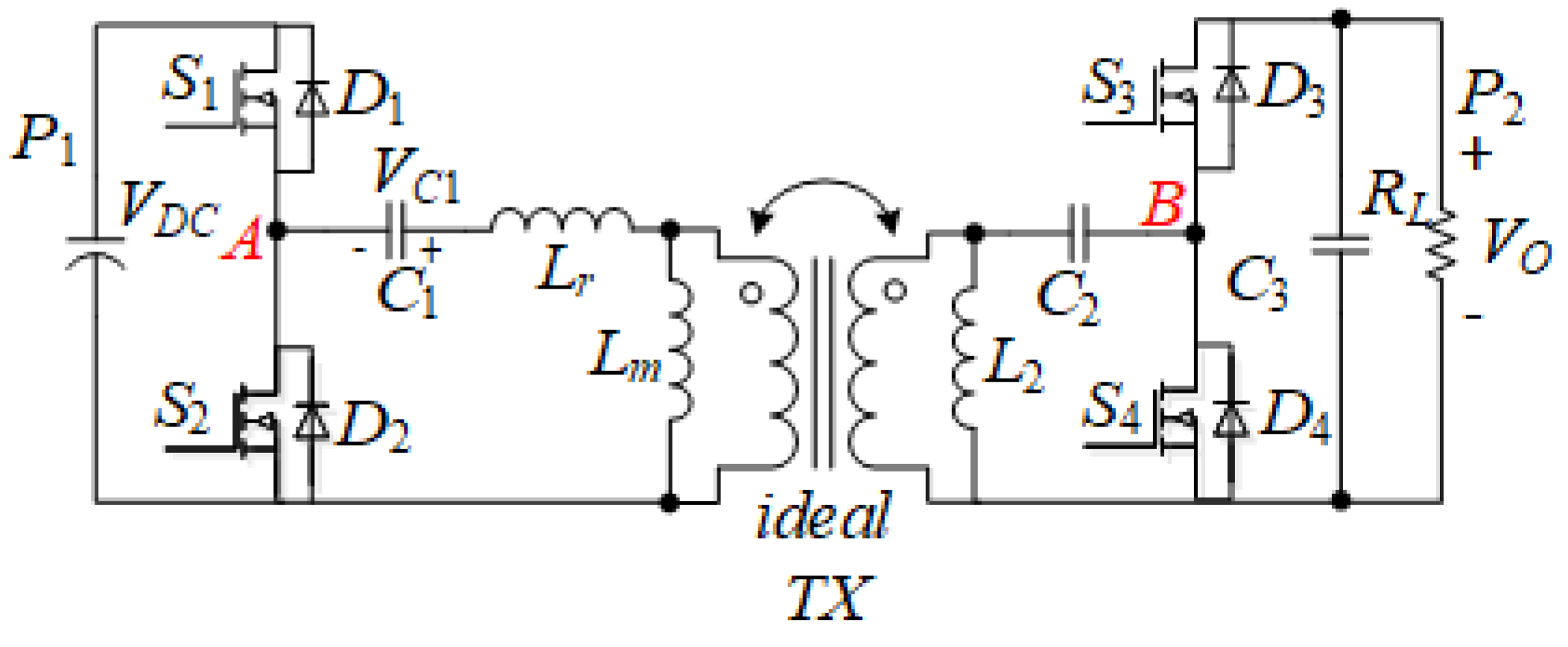
3. Power Stage Analysis

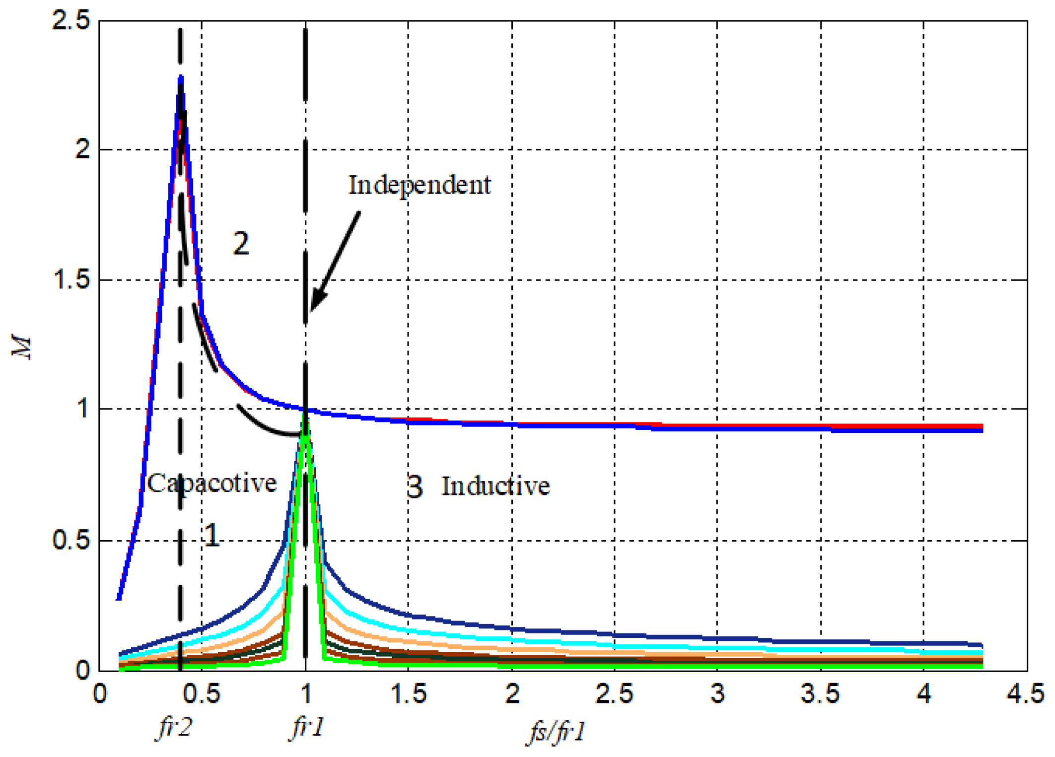
3.1. Resonant Analysis

In order to realize bidirectional power transfer, the symmetrical half-bridge resonant topology is chosen in this system, and a series resonant network in both the sanding side and receiving side is used for the air-coupled power transfer. To facilitate the analysis, the system can be simplified to an LLC series resonant two-port network shown in Figure 2, by converting all the impedance to the sending side.
In the simplified series resonant network shown above, C r is the series resonant capacitor (equivalent to the capacitance C 1 in schematic diagram), L r is the leakage inductance of the air coupling transformer, L m is the magnetizing inductance and Z a c is the equivalent impedance of the transformer. The ralationship between L 1 , L r and L m is show as (1).
L 1 = L r + L m
This resonant network has two resonant frequency, the first resonant frequency f r 1 and the second resonant frequency f r 2 .
f r 1 = 1 2 π L r C r
f r 2 = 1 2 π C r ( L r + L m )
In this design the ratio of the air-coupled transformer is set to 1, so the relationship between output voltage U o and input voltage U i n can be obtained as (4).
U o U i n = j ω Z o j ω L m + Z o 1 j ω C r + j ω L m + j ω Z o j ω L m + Z o
where Z o is the output characteristic impedance. We suppose λ = L r / L m to be the ratio between leakage inductance L r and magnetizing inductance L m , and f n = f s /f r 1 is set to be the ratio between the switch frequency f s and the first resonant frequency f r 1 . Supposing that the system quality Q = Z o P o u t /U o u t 2 . The simplified function of the output voltage gain can be by introducing the impedance λ , f n and Q into (4).
M ( f n , λ , Q ) = 1 ( 1 + λ λ f n ) + Q 2 ( f n 1 f n )
Hence, the characteristic of the output voltage ratio against the operation frequency ratio under the different value of Q can be easily concluded as Figure 3.
According to Figure 3, the system can be divided into three different working modes based on the operating frequency: inductive working mode (f s > f r 1 ), load independent working mode (f s = f r 1 ) and capacitive working mode (f r 2 < f s < f r 1 ). In this proposal, considering the safety of the system, the operating frequency is set to be bigger than f r 1 .

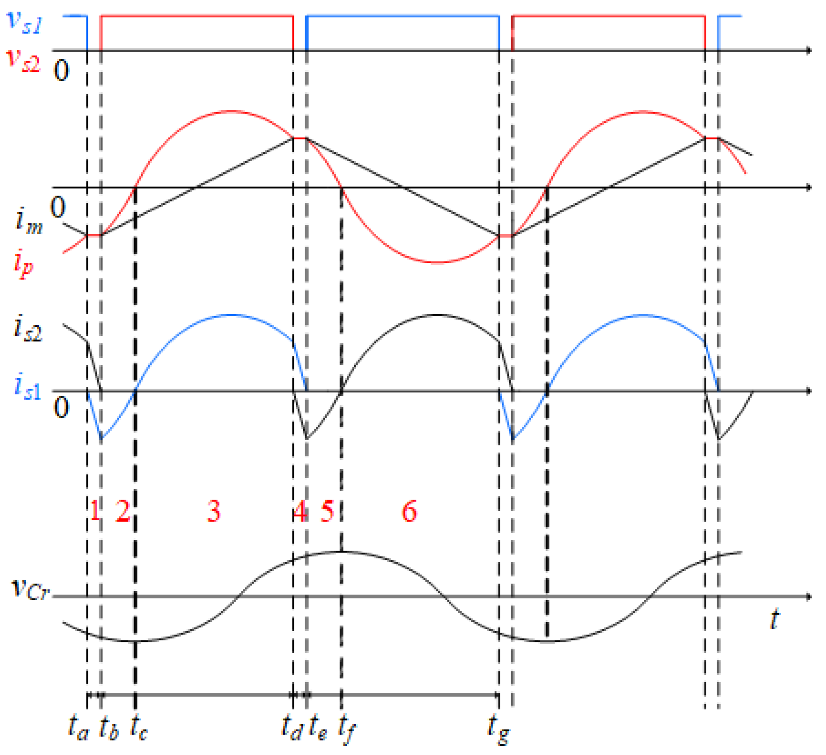
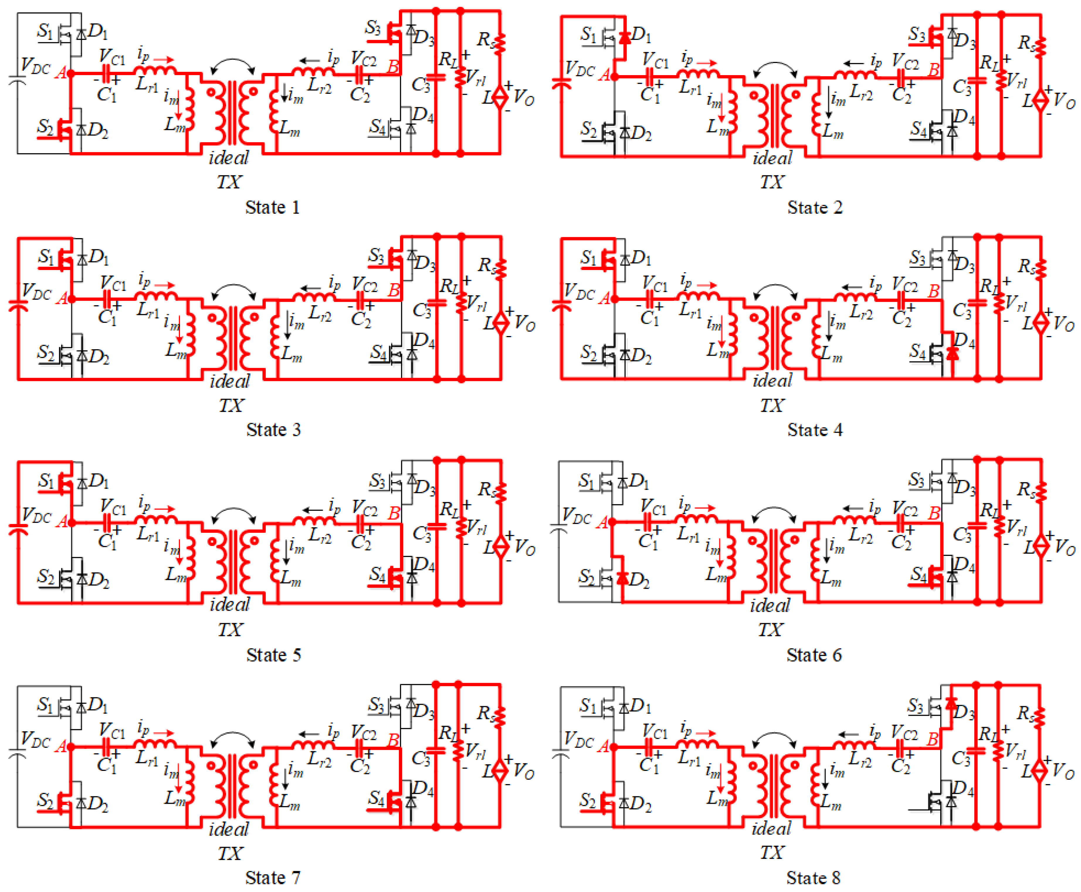
3.2. Forward Transfer Mode Analysis

To analyse the forward power transfer mode, considering that the system is working under very high switch frequency, it can be equivalent as the half-bridge LLC resonant converter shown in Figure 4; the output port P 2 is connected to the resister to simulate the load, and the driver signal is only given to switch S 1 and S 2 in complementary mode, the half-bridge combined by S 3 and S 4 working as an uncontrolled rectifier, power flows from P 1 to P 2 .
To realize the linear control of the transfer power, the frequency of the driving signal on S 1 and S 2 should be higher than the first resonant frequency: f s > f r 1 . In this case, the system can be divided into six working modes in a switching cycle. The theoretical waveform is shown in Figure 5. Where v s 1 and v s 2 are the driving signal of the switch S 1 and S 2 , i p is the current in the leakage inductance L r , i s 1 and i s 2 are the currents flowing in the switches S 1 and S 2 , respectively; v C 1 is the voltage on the resonant capacitor C 1 .
The following analysis is based on this case and the switch cycle time can be analyzed in six modes from t a to t g . Figure 6 shows the state diagram of the six working modes.
Model 1: Period between t a and t b , this period is the dead time of the driver signals, S 1 and S 2 are in the off state; in the primary side of the air coupled transformer, the current i p is reverse, and it flows through the anti-parallel diode D 1 of S 1 , thus, the zero voltage switching (ZVS) of S 1 realized. In the second side, the resistor is powered by the output capacitor C 3 , and the coupled current flows through the inductance L 2 capacitor C 2 and D 4 , thus, the second side is divided into two loop cells.
Model 2: Period between t b and t c , in this mode switch S 1 on, S 2 off. The current i p runs through the switch S 1 in forward direction and increasing, at the same time, the current i m increases linearly, the output power is supported by the coupled power. Assuming that the dead time is negligible, the current i p is calculated as (6).
i p ( t ) = i p ( t b ) c o s ω r 1 ( t t b ) + V b Z r 1 s i n ω r 1 ( t t b )
where i (t b ) is the current value on L r at time t b , V b is the voltage on L r , w r 1 is the angular frequency of the system, V C 1 is the voltage on the resonant capacitor C 1 , and V D f is the voltage drop of the diode D 3 .
i p ( t b ) = ( V o + V D f ) L m 1 ( T s / 4 Δ / 2 )
V b = V i n V C 1 ( t b ) ( V o + V D f )
Δ = t d t c = t g t f , ω r 1 = 2 π f r 1
In this case, the current in magnetizing inductance L m rises linearly in the forward direction, can be calculated as (10).
i m ( t ) = i m ( t b ) + n ( V o + V D f ) L m ( t t b ) = ( V o + V D f ) L m ( t t b T s 4 + Δ 2 )
where i m (t b ) = i p (t b ), T s is the switching period, in this working state, the resonant network includes the series L r and C 1 , and L m is out of the resonance. The current i p and i m will become the same value at the end of this working state, and the current in the diode D 3 will become zero. If the switching frequency f s = f r 1 , than Δ = 0 .
Model 3: Period between t c and t d . At the end of Model 2, i p = i m , and the current in D 3 is zero. Thus, in this mode, L 2 , C 2 and D 4 form an independent loop that is isolated from the output load, the resistor is powered by the output capacitor C 3 . In this mode, L m is involved in resonance, and the current i p and i m are equal. Therefore, we can calculate the current i p as (11):
i p ( t ) = i p ( t c ) Z r 2 C r c o s ( ω r 2 ( t t c ) ) + V C r ( t c ) Z r 2 s i n ω r 2 ( t t c )
Model 4 to Model 6 are working in the opposite state. In summary, it can be seen that the working mode of operation in Model 1 to Model 3 is symmetrical with respect to Model 4 to Model 6.

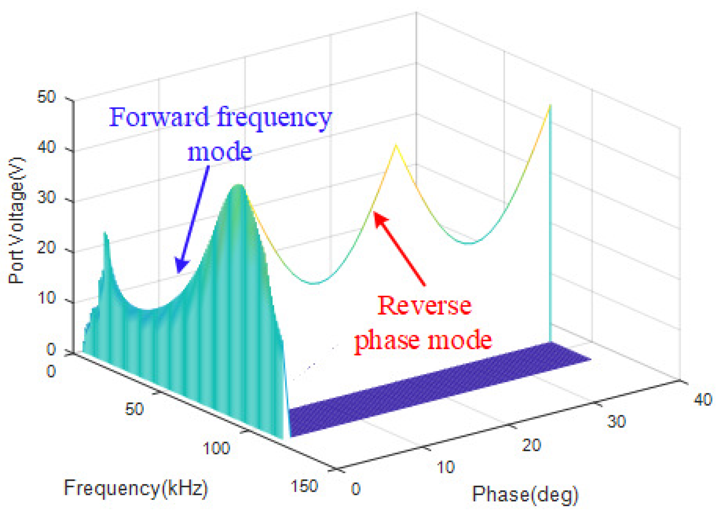
3.3. Reverse Power Transfer Mode Analysis

In the reverse power transfer mode, the input port P 1 connects to a 48 V DC grid and output port P 2 is connected to the source load, a resistor in parallel with a controlled voltage source is used to simulate the generation load, the equivalent circuit is shown in Figure 7.
This way, the power flows from P 2 to P 1 . Due to the high-frequency working situation, the system is working under the phase control mode which can be seen as a dual active bridge, where L r 1 is the leakage inductance of the primary side while L r 2 is the leakage inductance of the second side, and L m is the magnetizing inductance of the transformer. A phase control method is proposed to control the power flow by controling the voltage of R L .
While the system is working, the switch S 1 to S 4 are driven at the same time, and the drive signals are complementary between S 1 and S 2 , S 3 and S 4 , a phase shift is between the signal of the S 1 and S 3 , S 2 and S 4 , thus, the system can be divided into eight states in a drive period, according to the state of the four switches and also including the direction of the current in L r 1 and L r 2 , take the direction from right to left as forward direction of the current in L r 1 and L r 2 , also as the voltage of the capacitor C 1 and C 2 . The diagram of the eight states is shown in Figure 8.
The qualitative analysis of these working state are proposed as follows.
State 1: S 1 off S 2 on; S 3 on S 4 off, there are two connected loops in the secondary side: (I) the resistor R L is powered by the controlled source; (II) the controlled source also powers the capacitor C 3 and the coupled net, and the current is decreasing in the forward direction. In the primary side only one loop is formed including L r 1 , L m , C 1 and S 2 . This way the source load transfer the power to the primary side.
State 2: S 1 off S 2 off; S 3 on S 4 off, the secondary side keeps the same as the State 1, with the current flows through S 3 instead of D 3 . In the primary side, the current flows through D 1 to transfer the power to DC grid, although in both sides the current continues to decrease in the forward direction. The power flow is transferred from the source load to the DC grid.
State 3: S 1 on S 2 off; S 3 on S 4 off. There are no changes on the secondary side loop. The primary side current change to flow through S 1 , and the loop changes to include S 1 instead of D 1 . In this state, the current of both sides first decreases to zero and then rises in the reverse direction. Thus, the simulate resistor is powered by both the DC grid and the source load.
State 4: S 1 on S 2 off; S 3 off S 4 off. The primary circuit state remains unchanged. in the second side, due to the shutdown of S 3 and the reverse direction of the current in L r 2 , two independent circuits are formed: (1) Capacitor C 3 and resistor R L are powered by source load; (2) Coupled current runs through L m , L r 2 , C 2 and D 4 , storing coupled power in the magnetizing inductance L m , this state is called a coupled power storing state, and there is no power that is transferred to the DC grid.
The working mode of State 5 to State 8 is in the opposite direction of State 1 to State 4. From the above analysis, the working mode of the reverse transfer mode is also symmetrical.

4. Control System Design

The control strategies of the system are decided by the load condition, if the load is a power consuming load, the system will work in forward power transfer mode, this mode, the driving signals are given to S 1 and S 2 , S 3 and S 4 are off and using their anti-parallel diodes as an uncontrolled half-bridge to realize to highest transfer efficiency, and the frequency control method has been applied to control the output voltage, the controller is designed based on the built mathematical model of this transfer mode.
If the output voltage is over and out of control by using a frequency control method, that means the load has changed into a generator load; thus, the system will change to the reverse power transfer mode, the driving signals will also be given to S 3 and S 4 , and the control method will be changed into the phase control method; the power will be controlled through controlling the port voltage (voltage on R L ). Hence, the mathematical model of the reverse power transfer mode has not been built yet and the convention PI controller will be applied.

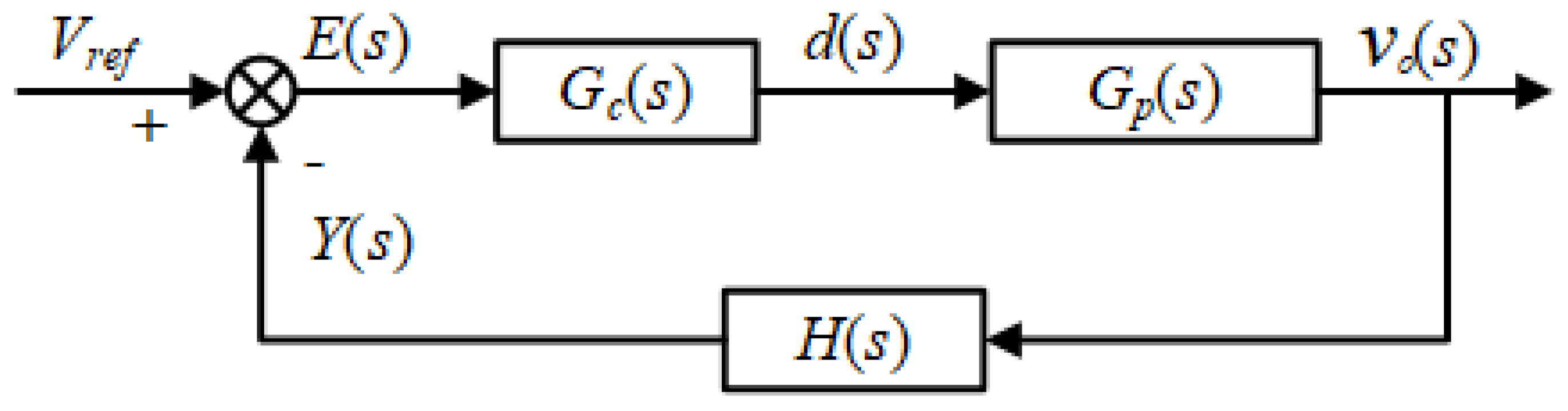
4.1. Small Signal Analysis

A frequency control method is proposed to control the output voltage of the forward power transfer. To realize the digital control of this system, a small signal model of the system is built, separating the output of the half-bridge inverter into a sine and a cosine voltage source, and the equivalent simplified circuit is shown in Figure 9.
Where r s represents the resistor of the coil, L S is the primary resonant inductance (i.e., the leakage inductance of the air coupled transformer), C S is the primary resonant capacitor (i.e., C 1 in Figure 4), r c is the equivalent resistor of the output capacitor, C f is the output capacitor (i.e., C 3 in Figure 4), and R is the output resistance.
The output voltage of the half-bridge can be divided into two parts, the sine voltage source v e s and the cosine voltage source v e c , i s is the current of the sine source and i c is the current of the cosine source, v e s and v e c can be obtained as (12) and (13), respectively.
v e s = L s ( d i s d t + ω s i c ) + r s i s + v s + v p s = L s ( d i s d t + ω s i c ) + r s i s + v s + 4 n π i p s i p p v c f
v e c = L s ( d i s d t + ω s i s ) + r s i c + v c + v p s = L s ( d i s d t + ω s i s ) + r s i c + v c + 4 n π i p c i p p v c f
Introducing the small signal into the state equation of the system, the plant transfer function G p (s) between the output voltage and frequency is obtained as (14). The parameters already been considered.
G p ( s ) = 5.5895 ( 1 + s 3.314 × 10 4 ) × ( s 8.262 × 10 5 1 ) ( s 2 + 973.6 s 8.949 × 10 8 + 1 ) × ( s 2 + 2.76 × 10 5 s 1.227 × 10 12 + 1 )

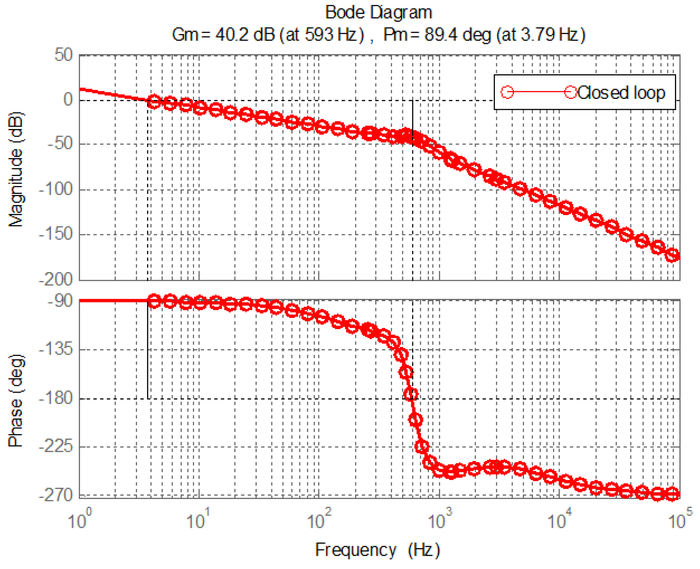
4.2. Forward Power Transfer Control Loop

For the forward power transfer, the voltage mode closed-loop control method is applied to control the power transmission. Considering the characteristics of the system, a frequency mode control method is proposed to control the output voltage. The control block diagram is shown in Figure 10. V r e f is the reference value, Y(s) is the output of feedback loop, G p (s) is the transfer function of the plant, the function between output voltage and switching frequency, G c (s) is the controller.
Considering the transfer function of the plant, the controller is designed as a two zeros and three poles controller. The testing and experimental method is applied to get the parameters of the controller, as is shown in (15).
G c ( s ) = 371249.6041 × ( s 2 + 973.6 s + 8.949 × 10 8 ) s × ( s + 3.314 × 10 4 ) × ( s + 1.03 × 10 6 )
The bode diagram can be easily obtained as shown in Figure 11, from which the crossing frequency of the system is 593 Hz, and the phase margin is 89.4 degrees, system stability requirement is satisfied and therefore the closed loop system can work stably.

4.3. Reverse Power Transfer Control Loop

For the reverse power transfer, the voltage of R L is considered to control the transmission power. A phase control method is proposed for the reverse power flow control by controlling the voltage of R L ; the closed loop control block diagram is shown in Figure 12, where V r e f is the set reference, Y(s) is the output of feedback loop, G(s) is the transfer function of the plant, the function between voltage on R L and phase shift, C(s) is the controller.
Since the model of G(s) has not been built yet, a conventional PI controller is applied in this control system. The transfer function of the PI controller is as (16).
C ( s ) = K P + K I s
The same method of the experimental method is used to obtain the parameters of the PI controller, as K P = 1 and K I = 150 satisfies the stability requirement of the system design.

4.4. System Working Strategy

In this proposal, the P 2 voltage is controlled by two main parameters, switching frequency f s and phase angle between driving signals. For the forward power transfer mode, f s is working under a specific range, when the load is getting lighter, the f s control is applied to control the output voltage; this mode is called LLC mode. When the voltage is out of control, or the power flow tends to be reversed, the control strategy is changed to phase control under the optimal frequency point. The system switches to reverse transfer mode as Dual Active Bridge mode (DAB). The idea of the system working strategy is shown in Figure 13.

5. PSIM/MATLAB System Simulation

5.1. Forward Open Loop System Simulation

In order to get the characteristics of the forward power transmission mode, an open-loop system model built in PSIM is proposed to sweep the switching frequency to obtain the system characteristics upon frequency. For the forward power transfer, only S 1 and S 2 are driven by the driven signal, S 3 and S 4 just in function as the half-bridge rectifier, output resistor R L = 8 Ohm, consider the parameters chosen, the first resonant frequency f r 1 = 225 kHz, and the second resonant frequency f r 2 = 80 kHz. Thus, sweeping the switching frequency between 0 Hz and 300 kHz, and the characteristic curve can be obtained as Figure 14.
From the figure, it can be easily seen that when the switching frequency is over f r 1 , the output voltage decreases as the switching frequency increases. Therefore, linear control of the output voltage can be realized in this interval.

5.2. Forward Closed Loop Simulation

In order to verify the correctness and accuracy of the controller, the closed loop system is built in MATLAB (R2017a, MathWorks, Inc, Natic, MA, USA). The reference output voltage 40 V, the output voltage and current waveform can be seen in Figure 15, and it can be concluded that the control system achieves the desired efficiency.

5.3. Reverse Open Loop System Simulation

In the reverse power transfer mode, the phase shift method is applied with S 3 and S 4 are driven together and ahead of the S 1 and S 2 drive signal. The open-loop simulation is built in PSIM to get the characteristic of the power transmission among phase shift. The parameter is the same as the forward simulation mode, and the load is changed to be the source load, 48 V DC load is connected to the output port. The simulation makes S 3 and S 4 drive signal lead ahead than the signal of S 1 and S 2 , scan the phase from 0 to 360 degrees, and the curve of the input and output power along with the phase is shown in Figure 16, and the curve of the voltage on R L shown in Figure 17.
It can be easily concluded that reverse power transfer happens in the interval of 0–180 degrees of the leading phase, also in the range 0–90 degrees, the power transmission increases with the phase degree increase, while it decreases in the range 90–180 degrees. However, the voltage on R L presents an opposite trend then the power transmission. Therefore, the interval of 0–90 degrees is chosen to be the limitation interval of the control system.

5.4. Reverse Closed-Loop Simulation

As the PI controller is applied, to verify the efficiency of the control parameters, the closed-loop system model is built in the MATLAB (R2017a, MathWorks, Inc, Natic, MA, USA). Set the reference of the voltage on R L be 45 V, the simulation waveform is shown in Figure 18. From the waveform, it can be shown that the control system achieves the desired efficiency.

5.5. Full System Simulation

The whole system is carried out in MATLAB, using the idea switch to change the resistor load to the source load. In order to verify the power control strategy, set the origin transfer direction to forward, and control the output voltage 30 V, change the load to source load at 0.6 s and control the voltage of R L 46 V; the simulation output waveform of the port voltage and the source load current is shown is Figure 19, from which the system function is verified.

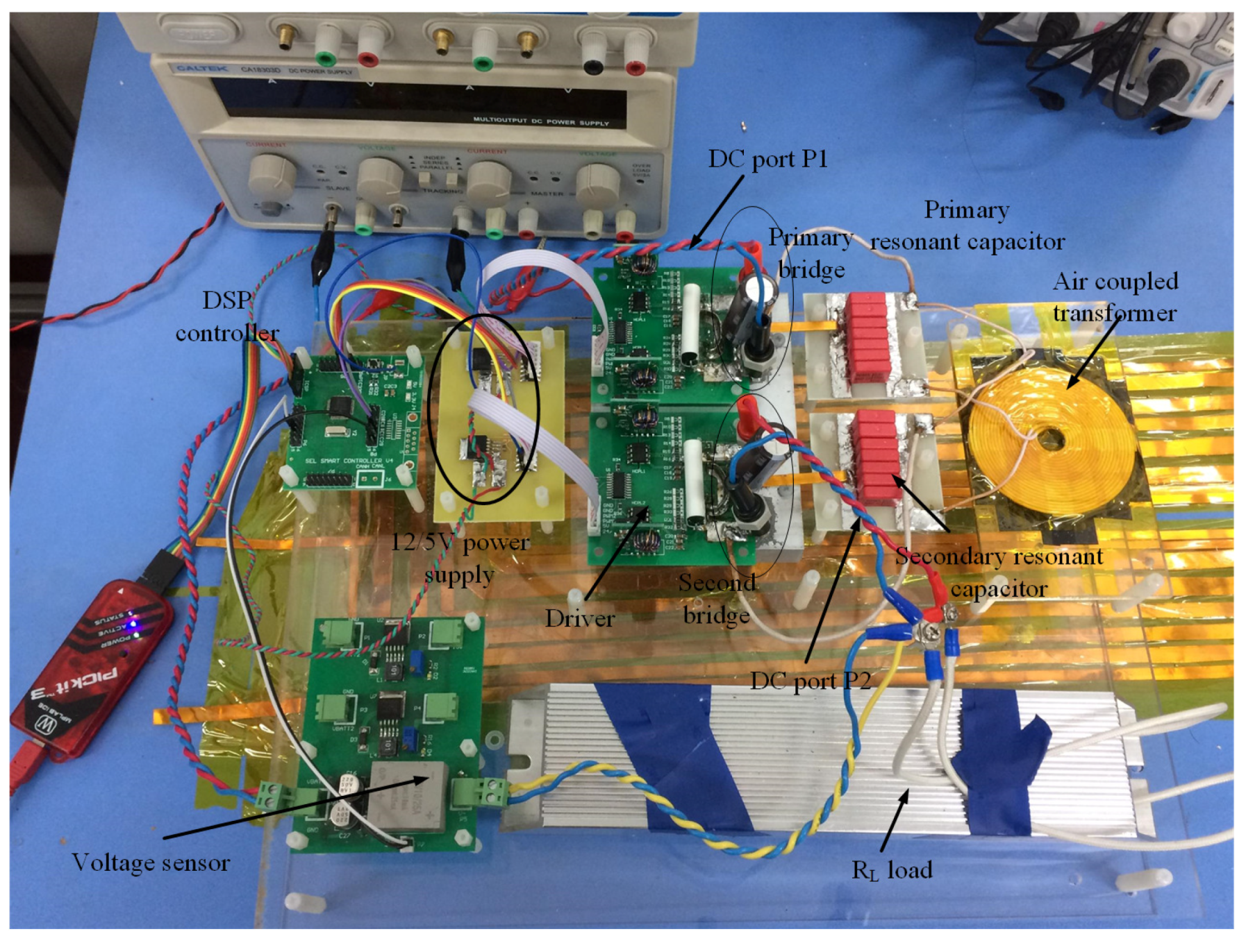
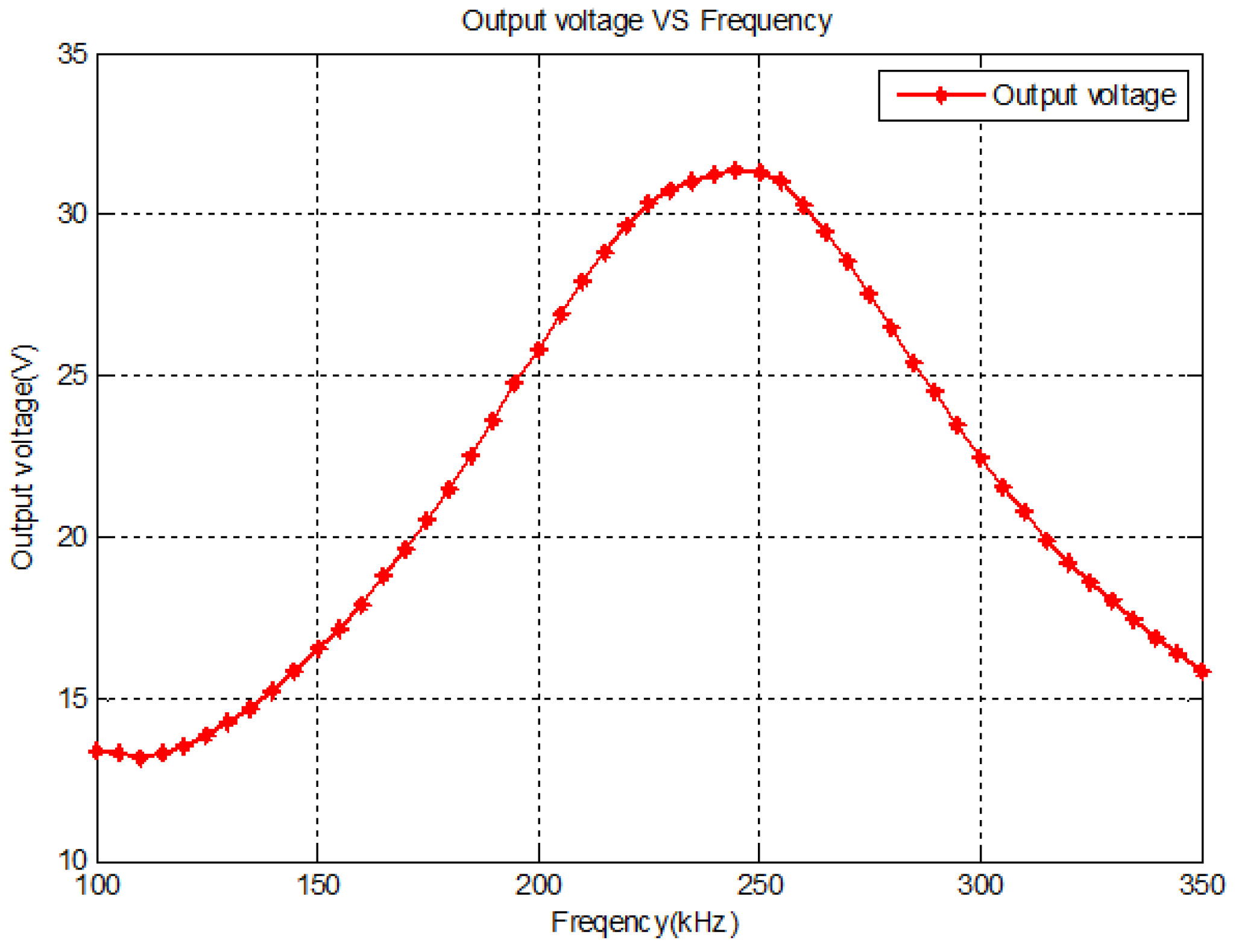
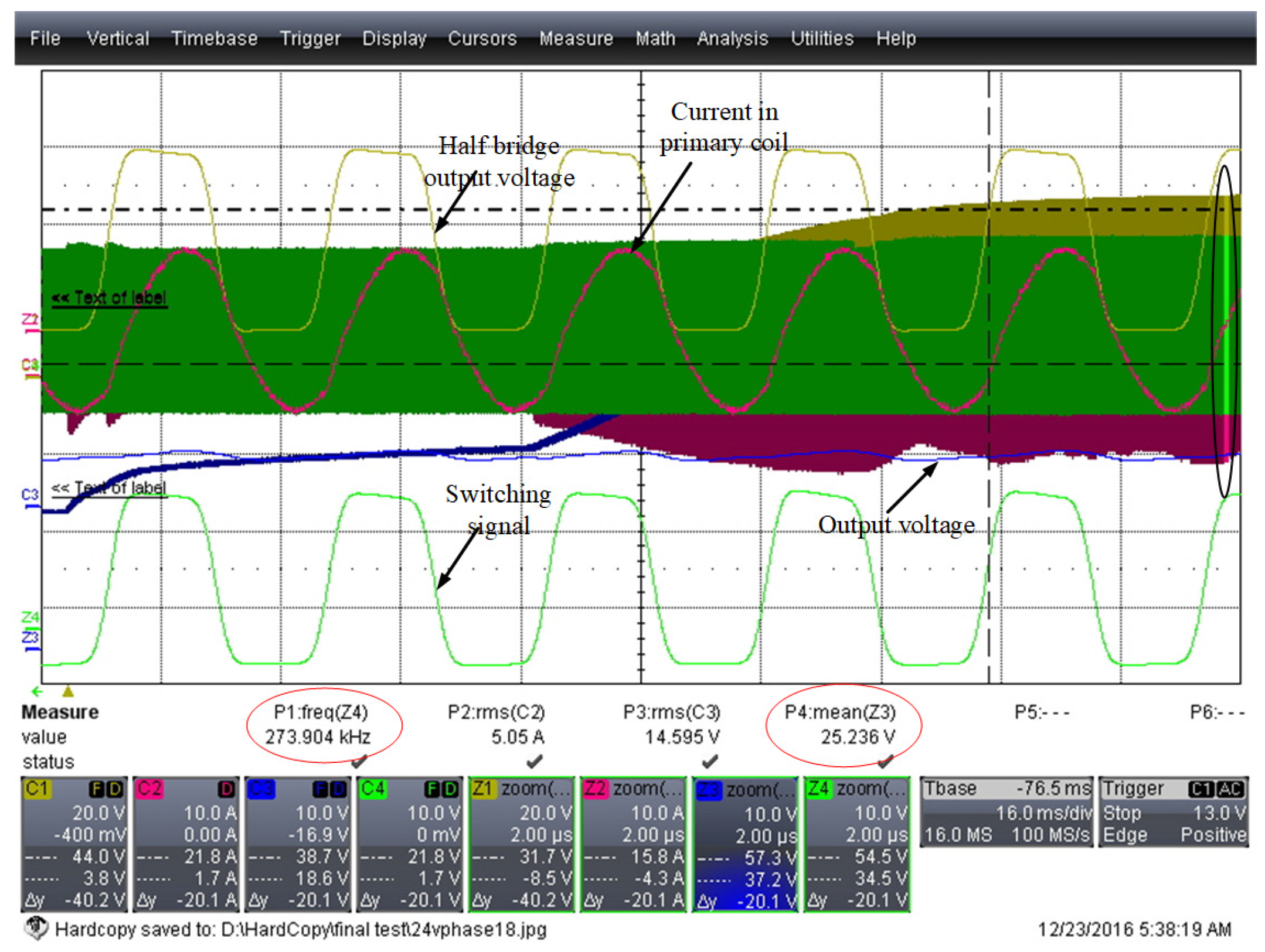
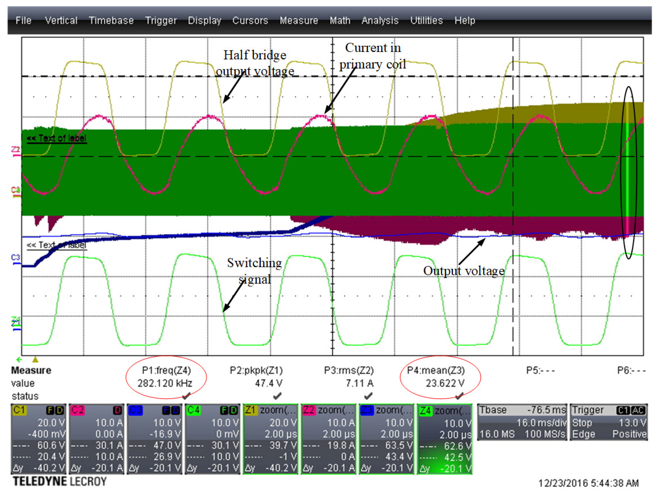
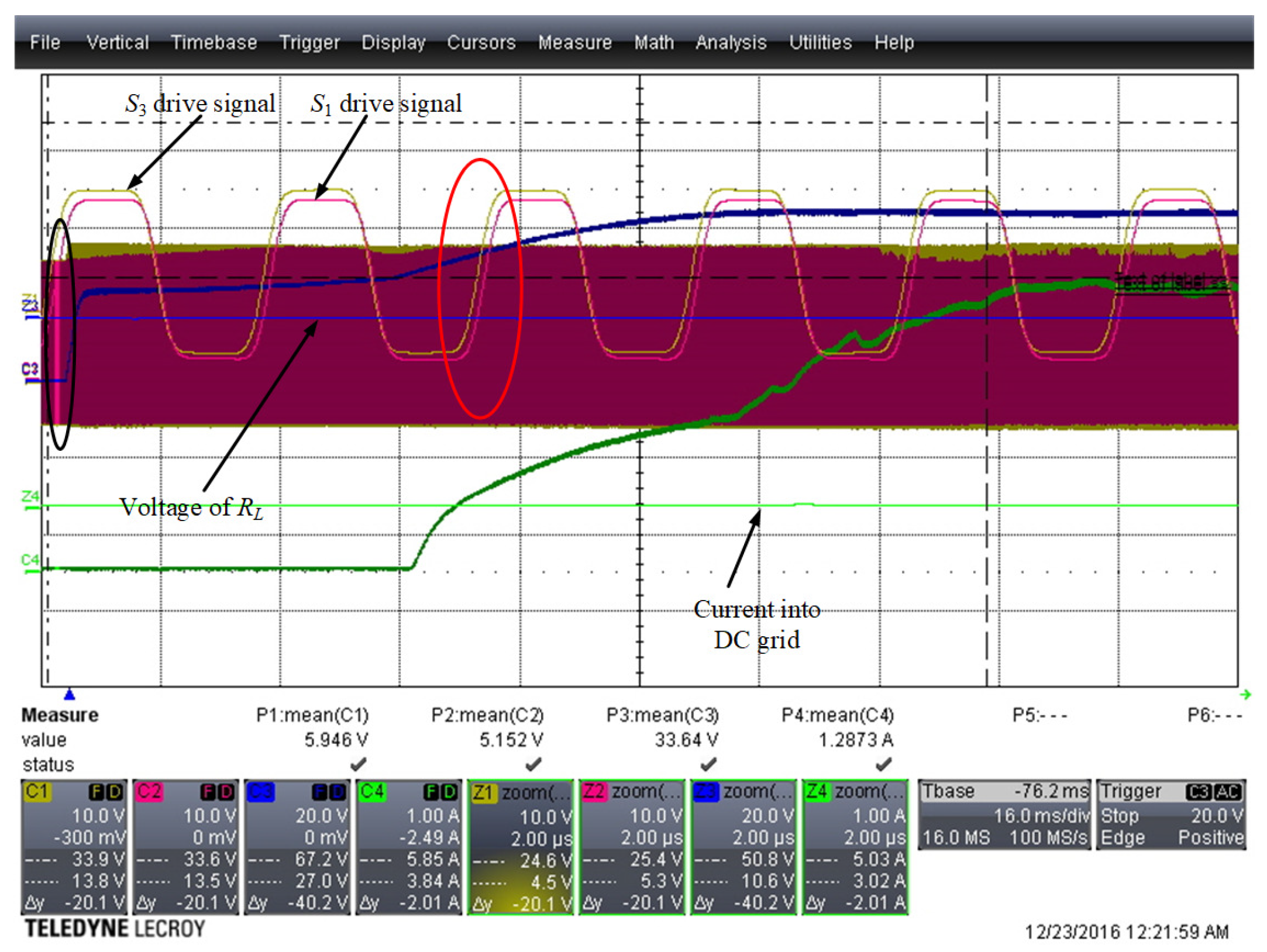
6. Experiments and Analysis

An experimental platform was built as shown in Figure 20, concluding the DC voltage source, air-coupled transformer and the simulated load of DC grid, and the parameters of the hardware system as listed in Table 1.
The experiments including the open-loop sweep and closed-loop experiment on both forward and reverse power flow transfer was carried out on this platform.

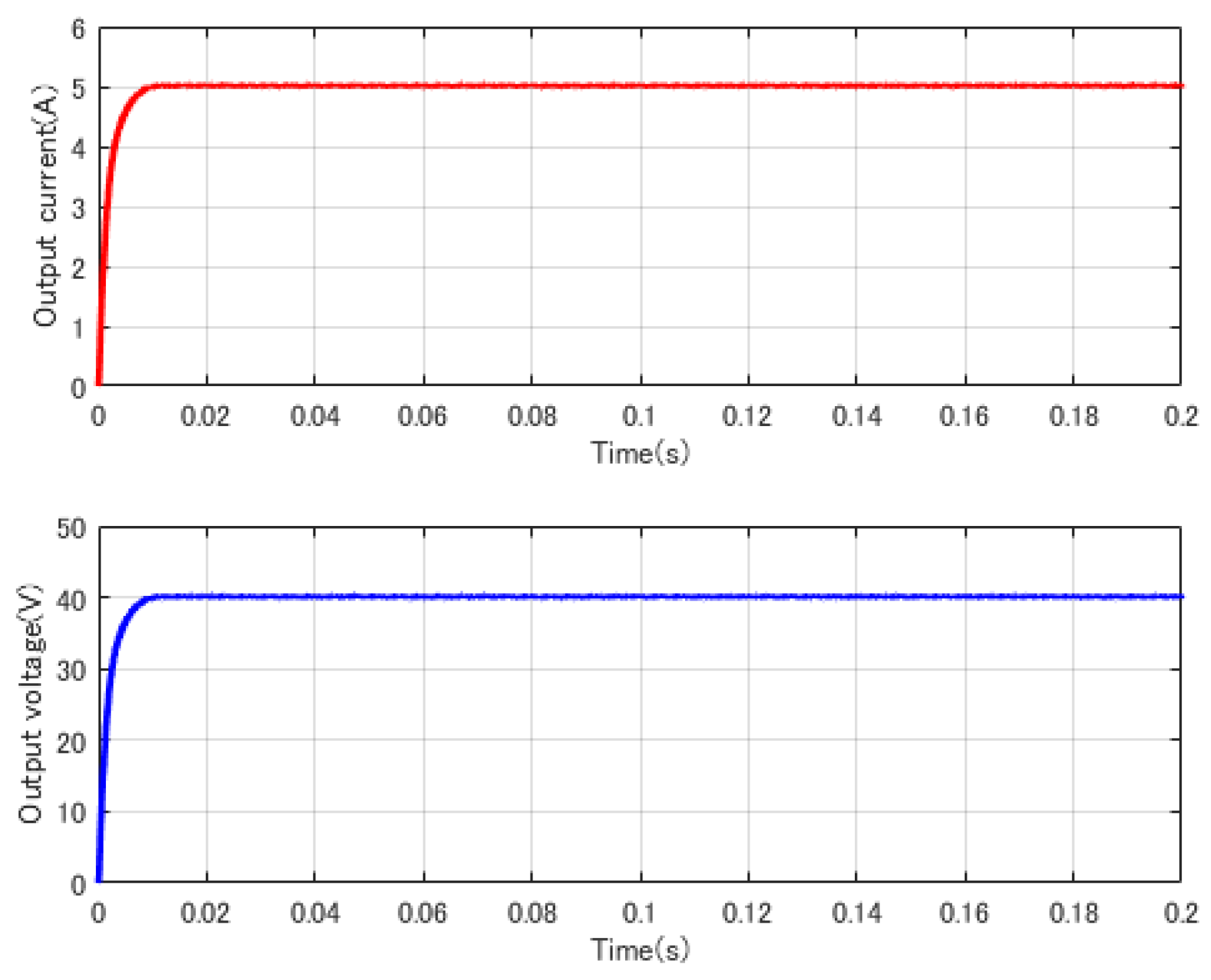
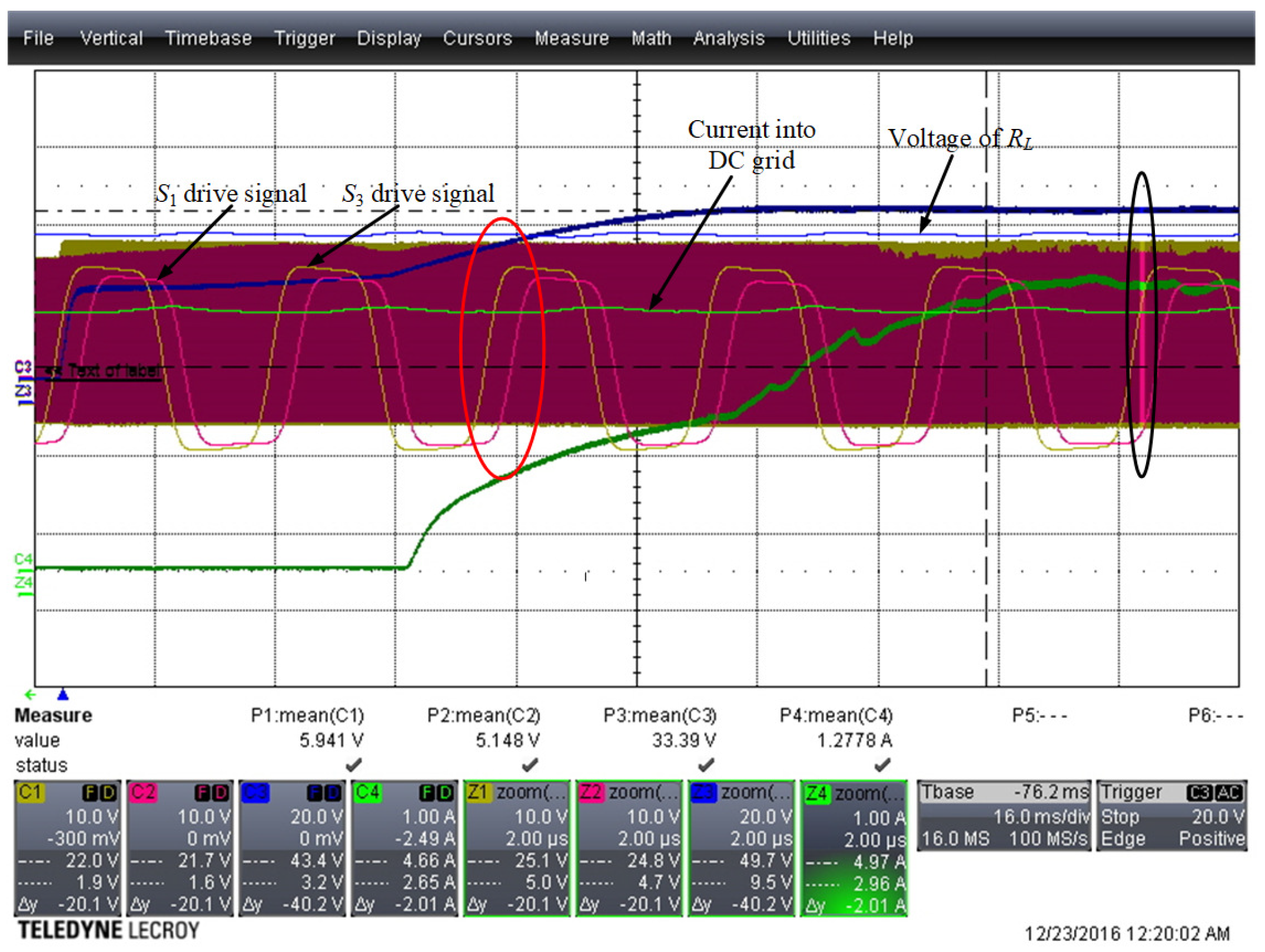
6.1. Forward Transfer Open Loop And Closed Loop Experiments

Based on the simulation results of the forward power transfer mode, the experiment of the frequency sweep is carried out. Considering the system parameters, set the switching frequency at the range of 100–350 kHz, and the output voltage curve can be obtained in Figure 21. The diagram is similar to the simulation results and the system characteristics are verified.
The closed-loop experiment is based on the open-loop sweep results, where the switching frequency setting is higher than the first resonant frequency. At the beginning, the initial frequency of the system is set to 244 kHz and the initial system waveform is shown in Figure 22, where the system frequency is 243.695 kHz.
As can be seen, a reverse voltage is applied to turn off the switch. To verify the effectiveness of the control system, control the system output voltage at 25 V and 23 V, respectively; the waveforms are shown in Figure 23 and Figure 24, respectively. From the waveforms, the output voltage is 25 V, the system switching frequency is 273.9 kHz, while the output voltage of 23 V and the frequency is 282.12 kHz. The results meet the open-loop sweep result. Therefore, the control system is efficient and verified.

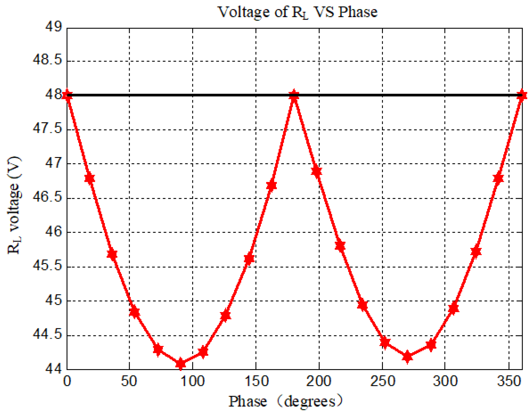
6.2. Reverse Transfer Open Loop and Closed Loop Experiments

This experiment is proposed to verify the bidirectional power transfer of the system; as in reverse power transfer mode, the switching frequency is higher than the first frequency. The drive signal of S 3 and S 4 leads the phase; sweep the phase from 30 degrees to 360 degrees under different switching frequency, the curve of the transfer power along with the phase can be obtained in Figure 25.
It can be easily concluded that before 90 degrees, the transfer power increases when the phase increases, while after 90 degrees, the trend becomes the opposite. Also, the frequency affects the power transmission; the closer to the first resonant frequency, the higher power transferred.
Choose the frequency at 280 kHz, and the phase control in the range of 0–90 degrees, set the initial phase at 20 degrees, the initial waveform of the drive signal of S 1 and S 3 , the voltage on R L and the current is shown in Figure 26.
To control the voltage of R L , set the reference voltage as 43 V and the waveform can be obtained in Figure 27, where the voltage on R L is 43.44 V, the phase is about 60 degrees, and the reverse transfer DC current is about 2.22 A, thus, the control system achieves the desired results.

7. Conclusions

In this paper, an air-coupled DC isolated transformer system is designed for the static and regenerative load in a DC microgrid. Considering the different load of the grid, bidirectional power transfer between the load and DC grid is realized. An integrated hybrid modulation control method is proposed to control the power flow: for forward power transfer, the frequency control stratagem is applied while for the reverse power transfer, the phase control method is used. The system characteristics of both forward and reverse power transfer modes are gained by a parameter sweep in open-loop simulation and experiments, and the control system verifying in closed loop simulation and experiments. The design has achieved expectations.

Author Contributions

Conceptualization, W.J. and S.X.; methodology, W.J. and S.X.; software, S.X.; validation, W.J., S.X. and S.H.; formal analysis, S.X.; investigation, S.H.; resources, W.J. and S.H.; data curation, S.X.; writing–original draft preparation, S.X.; writing–review and editing, W.J.; visualization, S.H.; supervision, S.H.; project administration, W.J.; funding acquisition, W.J. and S.H.

Funding

This research was jointly supported by Natural Science Foundation of China (Grant No. 31571765) and Yangzhou City-Yangzhou University joint Grant (No. SCX2017020021).

Conflicts of Interest

The authors declare no conflict of interest.

References

  1. Zheng, H.; Ma, H.; Ma, K.; Bo, Z. Modeling and analysis of the AC/DC hybrid micro-grid with bidirectional power flow controller. In Proceedings of the 2017 China International Electrical and Energy Conference (CIEEC), Beijing, China, 25–27 October 2017; pp. 280–284. [Google Scholar]
  2. Chen, Z.; Wang, K.; Li, Z.; Zheng, T. A review on control strategies of AC/DC micro grid. In Proceedings of the 2017 IEEE International Conference on Environment and Electrical Engineering and 2017 IEEE Industrial and Commercial Power Systems Europe (EEEIC/I&CPS Europe), Milan, Italy, 6–9 June 2017; pp. 1–6. [Google Scholar]
  3. Kakigano, H.; Miura, Y.; Ise, T.; Uchida, R. DC Voltage Control of the DC Micro-grid for Super High Quality Distribution. In Proceedings of the 2007 Power Conversion Conference, Nagoya, Japan, 2–5 April 2007; pp. 518–525. [Google Scholar]
  4. Liu, B.; Zhuo, F.; Zhu, Y.; Yi, H. System Operation and Energy Management of a Renewable Energy-Based DC Micro-Grid for High Penetration Depth Application. IEEE Trans. Smart Grid 2015, 6, 1147–1155. [Google Scholar] [CrossRef]
  5. Davari, M.; Mohamed, Y.A.I. Robust Multi-Objective Control of VSC-Based DC-Voltage Power Port in Hybrid AC/DC Multi-Terminal Micro-Grids. IEEE Trans. Smart Grid 2013, 4, 1597–1612. [Google Scholar] [CrossRef]
  6. Zhang, Y.; Lu, T.; Zhao, Z.; He, F.; Chen, K.; Yuan, L. Selective Wireless Power Transfer to Multiple Loads Using Receivers of Different Resonant Frequencies. IEEE Trans. Power Electron. 2015, 30, 6001–6005. [Google Scholar] [CrossRef]
  7. Zhang, Y.; Chen, K.; He, F.; Zhao, Z.; Lu, T.; Yuan, L. Closed-Form Oriented Modeling and Analysis of Wireless Power Transfer System With Constant-Voltage Source and Load. IEEE Trans. Power Electron. 2016, 31, 3472–3481. [Google Scholar] [CrossRef]
  8. Zhang, Y.; Zhao, Z.; Chen, K. Frequency Decrease Analysis of Resonant Wireless Power Transfer. IEEE Trans. Power Electron. 2014, 29, 1058–1063. [Google Scholar] [CrossRef]
  9. Dai, J.; Ludois, D.C. A Survey of Wireless Power Transfer and a Critical Comparison of Inductive and Capacitive Coupling for Small Gap Applications. IEEE Trans. Power Electron. 2015, 30, 6017–6029. [Google Scholar] [CrossRef]
  10. Zhong, W.; Hui, S.Y.R. Auxiliary Circuits for Power Flow Control in Multifrequency Wireless Power Transfer Systems With Multiple Receivers. IEEE Trans. Power Electron. 2015, 30, 5902–5910. [Google Scholar] [CrossRef]
  11. Kurs, A.; Karalis, A.; Moffatt, R.; Joannopoulos, J.D.; Fisher, P.; Soljai, M. Wireless power transfer via strongly coupled magnetic resonances. Sci. Express 2007, 317, 83–86. [Google Scholar] [CrossRef]
  12. Lu, F.; Zhang, H.; Hofmann, H.; Mi, C.C. An Inductive and Capacitive Combined Wireless Power Transfer System with LC-Compensated Topology. IEEE Trans. Power Electron. 2016, 31, 8471–8482. [Google Scholar] [CrossRef]
  13. Berger, A.; Agostinelli, M.; Vesti, S.; Oliver, J.A.; Cobos, J.A.; Huemer, M. A Wireless Charging System Applying Phase-Shift and Amplitude Control to Maximize Efficiency and Extractable Power. IEEE Trans. Power Electron. 2015, 30, 6338–6348. [Google Scholar] [CrossRef]
  14. Li, H.; Fang, J.; Chen, S.; Wang, K.; Tang, Y. Pulse Density Modulation for Maximum Efficiency Point Tracking of Wireless Power Transfer Systems. IEEE Trans. Power Electron. 2018, 33, 5492–5501. [Google Scholar] [CrossRef]
  15. Liu, F.; Yang, Y.; Jiang, D.; Ruan, X.; Chen, X. Modeling and Optimization of Magnetically Coupled Resonant Wireless Power Transfer System with Varying Spatial Scales. IEEE Trans. Power Electron. 2017, 32, 3240–3250. [Google Scholar] [CrossRef]
  16. Nguyen, M.Q.; Chou, Y.; Plesa, D.; Rao, S.; Chiao, J. Multiple-Inputs and Multiple-Outputs Wireless Power Combining and Delivering Systems. IEEE Trans. Power Electron. 2015, 30, 6254–6263. [Google Scholar] [CrossRef]
  17. Huang, M.; Lu, Y.; Martins, R.P. A Reconfigurable Bidirectional Wireless Power Transceiver for Battery-to- Battery Wireless Charging. IEEE Trans. Power Electron. 2019, 34, 7745–7753. [Google Scholar] [CrossRef]
  18. Huang, C.; Lin, C. Wireless Power and Bidirectional Data Transfer Scheme for Battery Charger. IEEE Trans. Power Electron. 2018, 33, 4679–4689. [Google Scholar] [CrossRef]
  19. Seo, D.; Lee, J.; Lee, H. Optimal Coupling to Achieve Maximum Output Power in a WPT System. IEEE Trans. Power Electron. 2016, 31, 3994–3998. [Google Scholar] [CrossRef]
  20. Lim, Y.; Park, J. A Novel Phase-Control-Based Energy Beamforming Techniques in Nonradiative Wireless Power Transfer. IEEE Trans. Power Electron. 2015, 30, 6274–6287. [Google Scholar] [CrossRef]
  21. Shin, S.; Shin, J.; Song, B.; Lee, S.; Kim, Y.; Jung, G.; Jeon, S. Wireless power transfer system for high power application and a method of segmentation. In Proceedings of the 2013 IEEE Wireless Power Transfer (WPT), Perugia, Italy, 15–16 May 2013; pp. 76–78. [Google Scholar]
  22. Sanborn, G.; Phipps, A. Standards and methods of power control for variable power bidirectional wireless power transfer. In Proceedings of the 2017 IEEE Wireless Power Transfer Conference (WPTC), Taipei, Taiwan, 10–12 May 2017; pp. 1–4. [Google Scholar]
  23. Qahouq, J.A.A.; Dang, Z. Investigation and simulation model results of high density wireless power harvesting and transfer method. In Proceedings of the 2017 IEEE Applied Power Electronics Conference and Exposition (APEC), Tampa, FL, USA, 26–30 March 2017; pp. 3095–3099. [Google Scholar]
  24. Zheng, H.; Wang, Z.; Li, Y.; Deng, P. Data transmission through energy coil of wireless power transfer system. In Proceedings of the 2017 IEEE PELS Workshop on Emerging Technologies: Wireless Power Transfer (WoW), Chongqing, China, 20–22 May 2017. [Google Scholar]
  25. Lee, C.H.; Jung, G.; Shin, S.; Kim, Y.; Song, B.; Shin, J.; Chung, S.H.; Kim, D.O.; Lee, J. Design and introduction of high power transfer system for electrical vehicles. In Proceedings of the 2013 IEEE International Conference on Intelligent Rail Transportation Proceedings, Beijing, China, 30 August–1 September 2013; pp. 280–284. [Google Scholar]
  26. Quenum, W.; Junqua, I.; Parmantier, J.P. Experimental power transfer and signal assessment of wireless communications in reverberating cavities. In Proceedings of the 2016 IEEE Wireless Power Transfer Conference (WPTC), Aveiro, Portugal, 5–6 May 2016; pp. 1–4. [Google Scholar]
  27. Lee, B.H.; Choi, Y.W.; Kim, B.C. Standby power reduction method for wireless power transfer system with parallel resonance type resonator. In Proceedings of the 2016 IEEE Wireless Power Transfer Conference (WPTC), Aveiro, Portugal, 5–6 May 2016; pp. 1–3. [Google Scholar]
  28. Xia, C.; Chen, R.; Liu, Y.; Liu, L.; Chen, G. Inhibition of current harmonics in LCL/LCC wireless power transfer system. In Proceedings of the 2017 IEEE PELS Workshop on Emerging Technologies: Wireless Power Transfer (WoW), Chongqing, China, 20–22 May 2017. [Google Scholar]
  29. Matias, R.; Cunha, B.; Martins, R. Modeling inductive coupling for Wireless Power Transfer to integrated circuits. In Proceedings of the 2013 IEEE Wireless Power Transfer (WPT), Perugia, Italy, 15–16 May 2013; pp. 198–201. [Google Scholar]
  30. Van der Pijl, F.F.A.; Bauer, P.; Castilla, M. Adaptive Sliding-Mode Control for a Multiple-User Inductive Power Transfer System without Need for Communication. IEEE Trans. Ind. Electron. 2013, 60, 271–279. [Google Scholar] [CrossRef]
  31. Van der Pijl, F.F.A.; Bauer, P.; Castilla, M. Control Method for Wireless Inductive Energy Transfer Systems With Relatively Large Air Gap. IEEE Trans. Ind. Electron. 2013, 60, 382–390. [Google Scholar] [CrossRef]
  32. Polinder, H.; van der Pijl, F.F.A.; de Vilder, G.-J. Comparison of direct-drive and geared generator concepts for wind turbines. IEEE Trans. Energy Convers. 2006, 21, 725–733. [Google Scholar] [CrossRef]
Figure 1. The proposed DC transformer: (a) System structure (b) System schematic.
Energies 12 02570 g001
Figure 2. Simplified two-port network.
Energies 12 02570 g002
Figure 3. Voltage gain vs. frequency ratio.
Energies 12 02570 g003
Figure 4. Forward equivalent circuit.
Energies 12 02570 g004
Figure 5. Theoretical waveform.
Energies 12 02570 g005
Figure 6. Forward working mode state diagrams.
Energies 12 02570 g006
Figure 7. Reverse equivalent circuit.
Energies 12 02570 g007
Figure 8. Reverse working mode state diagram.
Energies 12 02570 g008
Figure 9. Small signal equivalent circuit.
Energies 12 02570 g009
Figure 10. Forward control loop diagram.
Energies 12 02570 g010
Figure 11. Close loop system bode diagram.
Energies 12 02570 g011
Figure 12. Reverse control loop diagram.
Energies 12 02570 g012
Figure 13. System working strategy.
Energies 12 02570 g013
Figure 14. Output voltage vs. frequency.
Energies 12 02570 g014
Figure 15. Output voltage and current waveform.
Energies 12 02570 g015
Figure 16. Input and output voltage vs. phase.
Energies 12 02570 g016
Figure 17. Voltage on R L vs. phase.
Energies 12 02570 g017
Figure 18. Output waveform of voltage on R L .
Energies 12 02570 g018
Figure 19. Voltage waveform of full system.
Energies 12 02570 g019
Figure 20. Experiment platform of the system.
Energies 12 02570 g020
Figure 21. Output voltage vs. frequency.
Energies 12 02570 g021
Figure 22. Original waveform of forward transfer.
Energies 12 02570 g022
Figure 23. Waveform of controlling output 25 V.
Energies 12 02570 g023
Figure 24. Waveform of controlling output 23 V.
Energies 12 02570 g024
Figure 25. Output power vs. phase under different frequency.
Energies 12 02570 g025
Figure 26. Original waveform of reverse transfer.
Energies 12 02570 g026
Figure 27. Waveform with R L voltage 43 V.
Energies 12 02570 g027
Table 1. System parameters.
ParametersQuantityValue
C 1 , C 2 Resonant capacitor0.7 μ F
L 1 , L 2 Coil self-inductance14.6 μ H
kCoupling coefficient0.865
L m Magnetizing inductance12.629 μ H
L r Leakage inductance1.971 μ H
RLoad resistor8 Ohm
f r 1 First resonant frequency225 kHz
f r 2 Second resonant frequency83 kHz
V D C Suply voltage source48 V DC
S 1 , S 2 , S 3 , S 4 Power CMOSRF540

