Article

Influence of Parasitic Parameters on DC–DC Converters and Their Method of Suppression in High Frequency Link 35 kV PV Systems

1
School of Electronic Information and Electrical Engineering, Shanghai Jiao Tong University, Shanghai 200240, China
2
Dongguan South Semiconductor Technology Co., Ltd., Dongguan 523808, Guangdong, China
*
Author to whom correspondence should be addressed.
Energies 2019, 12(19), 3743; https://doi.org/10.3390/en12193743
Submission received: 2 September 2019 / Revised: 23 September 2019 / Accepted: 25 September 2019 / Published: 30 September 2019
(This article belongs to the Section A2: Solar Energy and Photovoltaic Systems)

Abstract

:
Photovoltaic (PV) power generation has shown a trend towards large-scale medium- or high-voltage integration in recent years. The development of high-frequency link PV systems is necessary for the further improvement of system efficiency and the reduction of system cost. In the system, high-frequency high-step-up ratio LLC converters are one of the most important parts. However, the parasitic parameters of devices lead to a loss of zero-voltage switching (ZVS) in the LLC converter, greatly reducing the efficiency of the system, especially in such a high-frequency application. In this paper, a high-frequency link 35 kV PV system is presented. To suppress the influences of parasitic parameters in the LLC converter in the 35 kV PV system, the influence of parasitic parameters on ZVS is analyzed and expounded. Then, a suppression method is proposed to promote the realization of ZVS. This method adds a saturable inductor on the secondary side to achieve ZVS. The saturable inductor can effectively prevent the parasitic elements of the secondary side from participating in the resonance of the primary side. The experimental results show that this method achieves a higher efficiency than the traditional method by reducing the magnetic inductance.

1. Introduction

Since PV power generation systems can alleviate the energy crisis and reduce environmental pollution, they have found broad application worldwide [1,2,3,4]. Traditional large-scale PV medium-voltage (MVAC) grid-connected systems mostly adopt centralized large-capacity inverters and line frequency transformers because of their simple structure and low installation cost [5,6,7]. The traditional structure of PV systems has achieved high efficiency and low cost. However, there are many problems in traditional systems, including mismatch power losses due to the limitations of single maximum power point tracking (MPPT) [8], magnetic loss and reactive power loss due to the line frequency transformer [9], and a massive consumption of material resources. As a result, the efficiency of traditional systems is difficult to improve any further. Although DC–DC converters can be introduced into the system, as described in [10], and additional power converters will allow each photovoltaic array to operate at its maximum power point (MPP), the remaining problems still cannot be solved, due to the use of the centralized inverter and line frequency transformer. With the development of wide band gap devices, high frequency isolation is possible, and PV systems with higher efficiency and power density are expected. To this end, many improved architectures have been proposed. In [11,12], a modular multilevel converter (MMC) was used to replace the line frequency transformer and central inverter in MVAC grid-connected systems. The MMC was able to easily achieve a medium voltage level, but it could not provide galvanic isolation of the photovoltaic array, and was not found to be suitable for PV systems. In [13], an isolated quasi-z-source DC–DC converter was employed in constructing a medium-voltage level DC bus and providing galvanic isolation for MMC. Nevertheless, controlling the whole system became more complex. Then, in [14], a cascaded H-bridge (CHB) multilevel converter was used to replace the MMC, and an isolated DC–DC converter was used to replace the line frequency transformer. In this architecture, the isolated DC–DC converter and the CHB module could easily be integrated into the PV system to improve the power-density of the system. Since the isolated DC–DC converter needs to undertake MPPT, its voltage gain may vary over a wide range, and its efficiency is difficult to improve. Furthermore, large-scale photovoltaic medium-voltage DC (MVDC) or high-voltage DC (HVDC) grid-connected systems are another promising direction in system structures [15,16]. In [17], a single-stage isolated DC–DC converter was used in an MVDC system, and the line frequency transformer was removed. This single-stage MVDC system was able to reduce system cost, power losses, and system bulk. However, its overall efficiency would be decreased by partial shading [18]. Hence, a two-stage DC–DC converter was used in an HVDC system in order to achieve higher frequency [19]. This paper is based on the high frequency link 35 kV PV system. The introduction of a high-frequency high-voltage isolated DC–DC converter is able to replace the line frequency transformer and save non-renewable resources. Therefore, the high-frequency high-voltage isolated DC–DC converter is one of the core technologies in PV systems.
Isolated high-frequency DC–DC converters can provide a fixed step-up ratio and galvanic isolation [19], and they constitute an important technology in PV power generation systems. A dual active bridge (DAB) was used early in PV applications because of its modular symmetric topological structure and fast dynamic response characteristics [20]. However, its ZVS range is limited by its voltage conversion ratio and load conditions. Therefore, it is difficult to achieve soft-switching throughout the full load range, and it is difficult to improve the efficiency any further [21]. In [22], a current source series resonant converter (SRC) was used as a DC–DC transformer (DCX). However, similar to DAB converters, it is difficult to implement ZVS throughout the full load range using an SRC. Recently, the LLC and CLLC topologies have become attractive due to their desirable characteristics, which include high efficiency, full load range ZVS, and zero-current-switching (ZCS) commutation [23,24,25]. Since bidirectional power flow is not a prerequisite in PV systems, CLLC converters are not suitable for improving power density. Therefore, LLC converters are the best choice.
However, there are still some problems presented by high-frequency LLC converters. On the one hand, unlike traditional low-voltage and low-frequency transformers, the insulation pressure of transformers in the converters makes the design of transformers and the selection of core materials more complex and more difficult [26]. On the other hand, the parasitic parameters of high-frequency transformer are complex, and these may have negative influences on the circuit. Furthermore, in recent years, SiC-MOSFETs have been widely used in DC–DC converters to pursue higher efficiency and higher power density [27]. Many studies have shown that SiC-based converters have greater advantages in terms of efficiency and power density compared to Si-based converters, especially in high-voltage applications [28,29,30]. However, both SiC-MOSFETs and SiC diodes have parasitic parameters. With the increase of the switching frequency of the LLC converter, the negative influences of parasitic parameters on the primary side ZVS of the high-frequency LLC converter gradually emerge [31,32]. In [33], the parasitic capacitor was investigated, and an optimized dead band was provided. In [34], the negative impacts caused by the parasitic capacitors of rectifier diodes were discussed. However, this only indicated negative influences on the DC voltage gain. In [31] and [35], the influence mechanism of parasitic parameters was investigated, and a solution was given in which the dead band and magnetic inductance were adjusted. However, the means for accurately selecting the dead band and magnetic inductance were not mentioned in those papers. The use of wide band gap devices can further improve the efficiency and power density of converters in PV systems. Unfortunately, without ZVS, the large switching losses and the deterioration of EMI characteristics caused by high switching frequency greatly reduces the performance of high-frequency LLC converters [36].
Therefore, this paper presents an architecture for the high frequency link 35 kV PV system, as shown in Figure 1. The distributed three-level boost converters with photovoltaic strings execute the MPPT algorithm. Isolated high-frequency DC–DC converters are used as DCXs between the CBH modules and a common DC bus. This paper studies the influence of parasitic parameters and theirmethod of suppression in high-frequency LLC converters in the 35 kV PV system. This paper describes how the parasitic parameters of SiC devices affect the ZVS of high-frequency LLC converters. Then, a method for suppressing the influence of parasitic parameters is proposed. By adding a saturable inductor on the secondary side, the parasitic components of the secondary side are effectively blocked from participating in the resonance of the primary side, and primary-side ZVS can be ensured. Finally, a multiple-pulse test (MPT) is carried out and a 2000 W small-scale experimental prototype is built to verify the theoretical analysis and suppression method. The experimental results show the proposed suppression methods are effective and the performance of the high-frequency LLC converter can be significantly improved.
Compared with the existing study, this work has some advantages:
  • The influence of the parasitic parameters of SiC devices in high-frequency LLC converters is analyzed step by step, which is more accurate.
  • The mechanism of influence of parasitic parameters on the resonance process is discussed systematically. The paper reveals how different parameters can affect the resonance process with respect to the parasitic parameters.
  • The proposed method is completely different from previous studies, and achieves better performance. Since the proposed method is able to achieve ZVS without a reduction in magnetic inductance and extension of the dead band, the efficiency can be further improved.
This paper is organized as follows. In Section 2, the high-frequency isolated cascaded MVAC grid-connected system is introduced. A downscaled system and its control method are provided. In Section 3, the analysis of influences of parasitic parameters are given, and the conventional suppression method by reducing magnetic inductance is analyzed. In Section 4, the proposed suppression method and its theoretical analysis are given. In Section 5, the theoretical analysis and proposed method are verified using the experimental prototype. Section 6 concludes the paper.

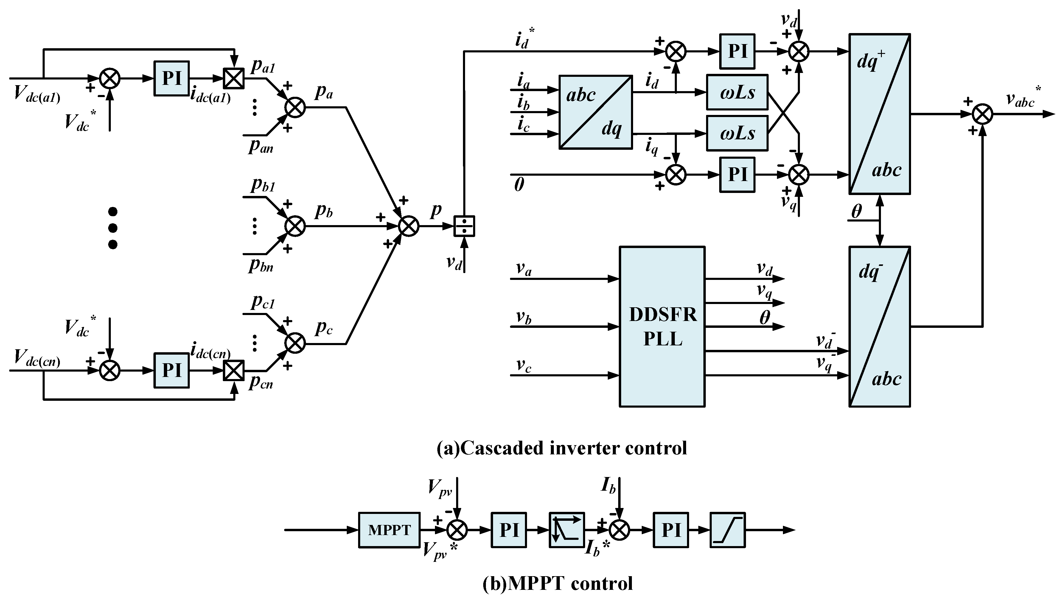
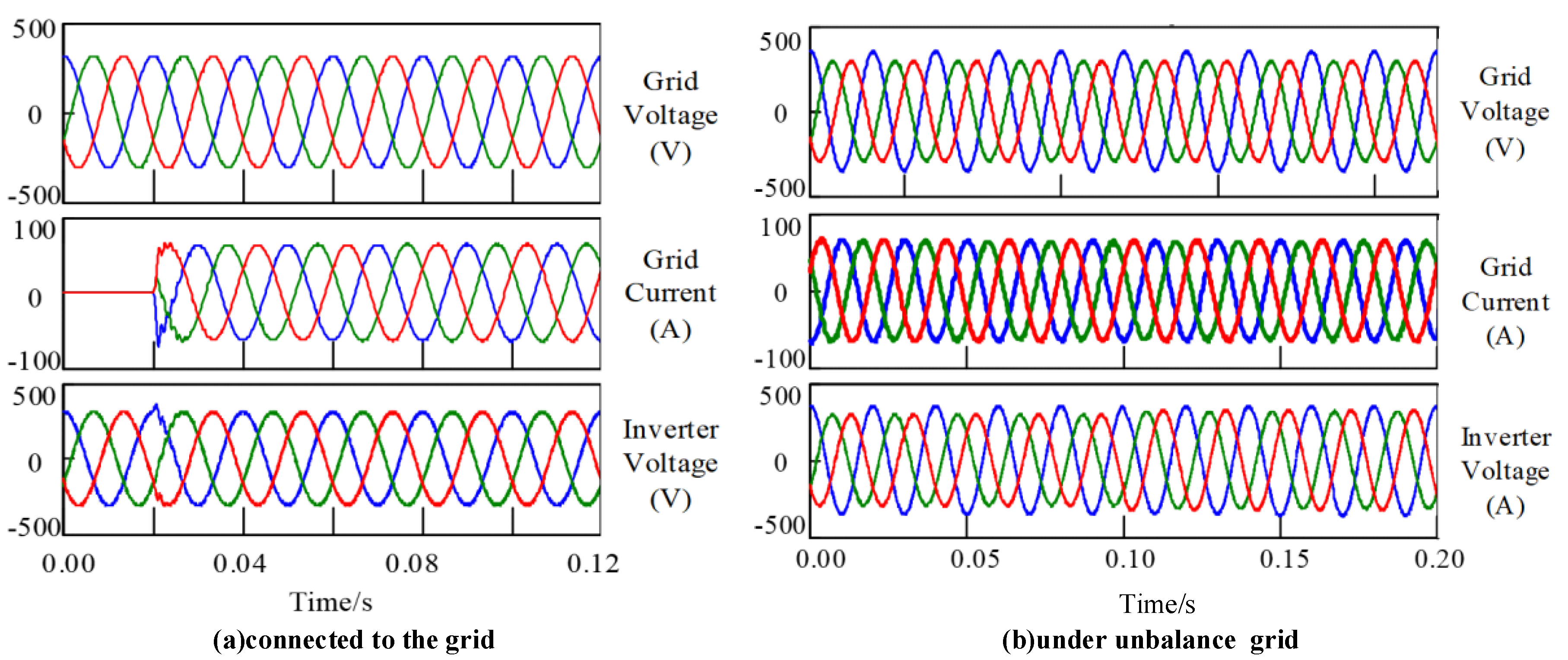
2. Architecture of High Frequency Link 35 kV PV System

The architecture of the presented high frequency link 35 kV PV system is shown in Figure 1. The system can be divided into three stages, including a distributed MPPT stage (non-isolated DC–DC converter), a DC–DC step-up stage (isolated DC–DC converter), and an inverter stage (cascaded inverter). The three-level boost topology is applied in the distributed MPPT stage. The three-level boost is responsible for MPPT, and is directly connected to the PV array. The output terminal of each converter is connected to the DC bus. The isolated DC–DC step-up stage uses a high-frequency LLC converter that works as DCX to provide galvanic isolation and a high step-up ratio. The inverter stage has a cascaded inverter topology. The CHB is used in this stage, which is directly connected to the MVAC grid.
In the presented system, a high-frequency isolated DC–DC converter is used to replace the line frequency transformer. The efficiency and power density can be increased. Additionally, copper consumption can be greatly reduced. The cascaded inverter replaces the centralized inverter. Thus, the switches can operate with lower frequency, lower switching losses and higher conversion efficiency.
The presented system is oriented towards 35 kV large-scale PV power generation. A 6 MW/35 kV PV system is designed based on the presented structure. The parameters of the system are shown in Table 1. To pursue higher efficiency and higher power density, SiC devices are used in the designed system because of their lower conduction loss and better performance under high temperature conditions, even though the switching frequency of CHB is very low. Then, according to the voltage level of the grid and devices, the number of CHB is determined to be 40. For high-frequency LLC converters, SiC devices are also used to achieve higher switching frequency and higher efficiency. In addition, in order to reduce the losses associated with single diodes, several diodes are connected in parallel on the secondary side of the LLC converter. For three-level boost, the devices can be selected to be the same as the LLC converter to reduce the number of different types of device. Besides, since there are a lot of symbols in the paper, all the symbols has been listed in the Appendix C as well.
The control scheme of the system is shown in Figure 2. Since an isolated DC–DC converter operates as the DCX, its voltage gain remains unchanged. As long as the output voltage remains stable, the DC bus voltage will be stabilized. Therefore, for controlling the cascaded inverter, the DC side voltage and the AC side power factor are the main control objectives, as shown in Figure 2a.
In Figure 2a, vdc(ki) (k = a, b, c and i = 1, 2, …, n) is the DC side voltage of unit(i) in phase k. The power reference of each CHB module pki is obtained by comparing vdc(ki) with the common reference vdc*. In the presented system, vdc* remains constant, despite the power variation required for controlling the DC bus voltage. Hence, it is possible to achieve a standard multilevel waveform with an equal and constant voltage level. The PI controller is used to control the power in the dq. When load imbalance or asymmetric faults occur, the grid voltage will be unbalanced. In this case, in addition to decoupling the power control, the cascade inverter also needs to control the balance of the current. In Figure 2a, vd, vd-, vq, vq- are the d-axis and q-axis components of the positive and negative sequence of the grid voltage respectively, and id, id-, iq, iq- are the d-axis and q-axis components of the positive and negative sequence of the grid current. These parameters can be obtained by using the phase-locked loop (PLL) based on the decouple double synchronous reference frames (DDSRF). Then, the three-phase current can be balanced by suppressing negative sequence current by feedforward negative sequence voltage of grid. For the MPPT stage, non-isolated DC–DC carries out MPPT shown in Figure 2b to improve the utilization of solar energy.
To verify the architecture and control scheme of the system, a downscaled system is built. The waveforms and the control effect of the 40 kW/380 V downscaled system are shown in Figure 3. Figure 3a shows the process of connection to the grid. It can be seen that the cascaded inverter can be connected to the grid quickly. Figure 3b shows the control effect of the control scheme discussed above. It is obvious that the control scheme of the system is able to suppress the negative sequence current and ensure the output current balance.
Although the downscaled system is able to operate well, there are still some problems that need to be solved in the experiment. The influence of parasitic parameters under high step-up ratio conditions is more serious, leading to the loss of ZVS. To achieve higher efficiency in high-frequency situations, it is necessary to study the influence of parasitic parameters and their suppression methods.

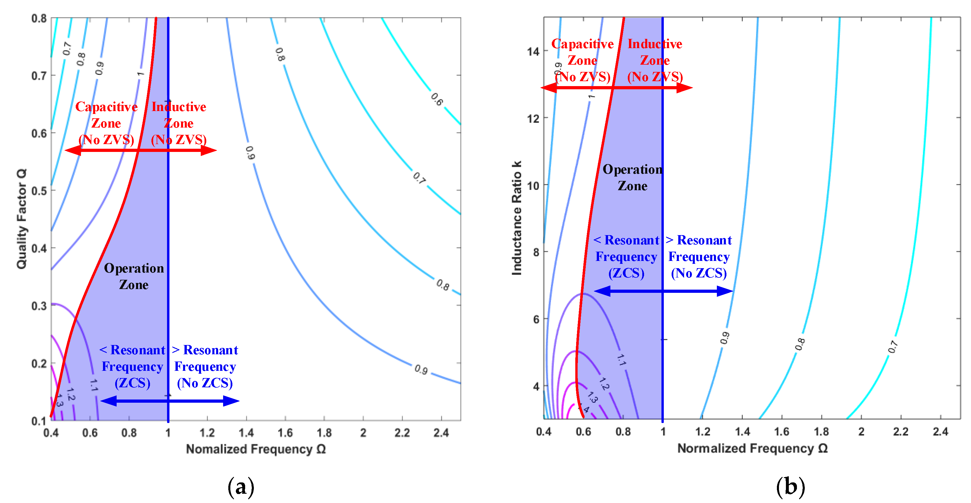
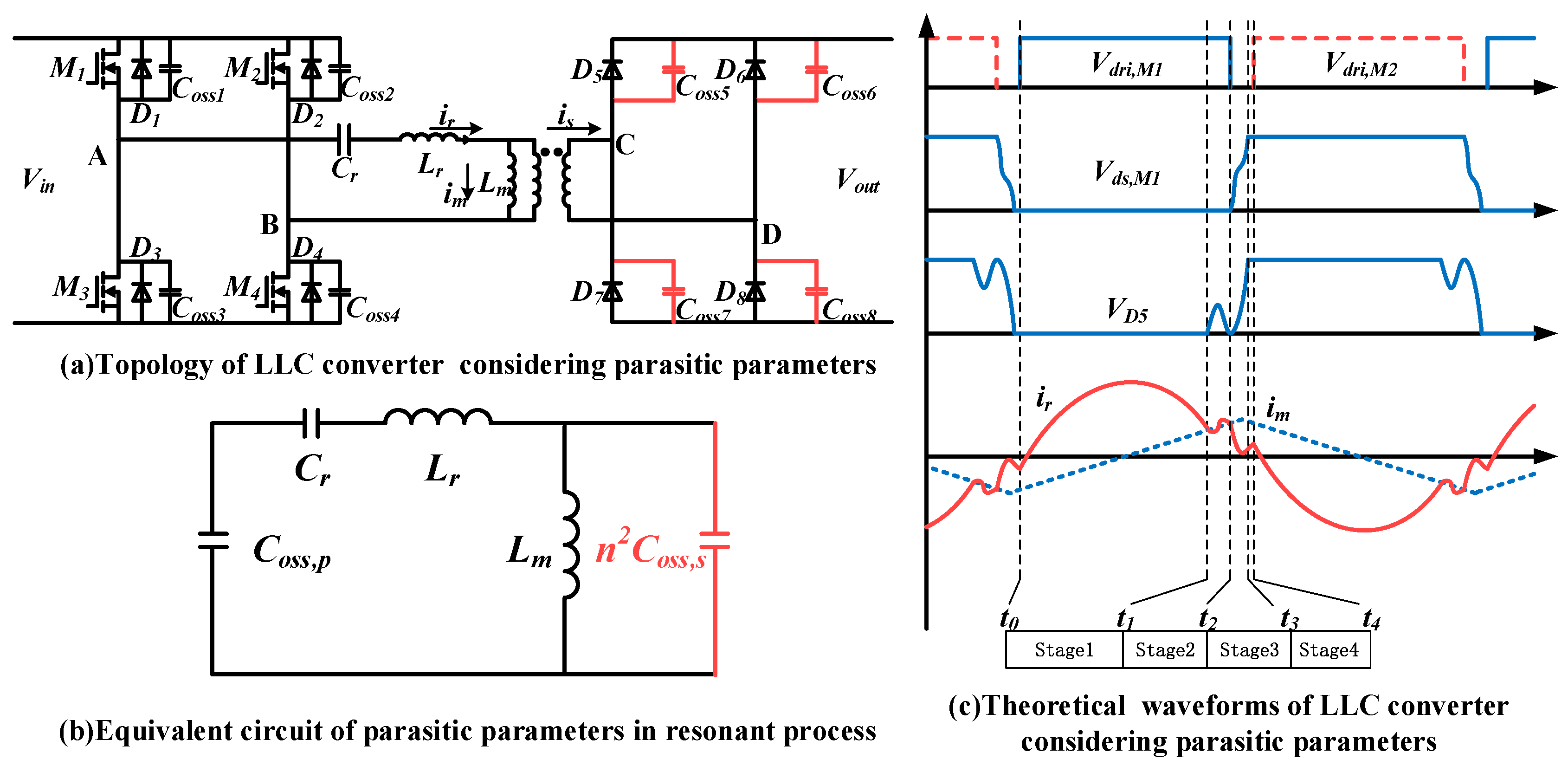
3. Influences of Parasitic Parameters on the Resonance Process

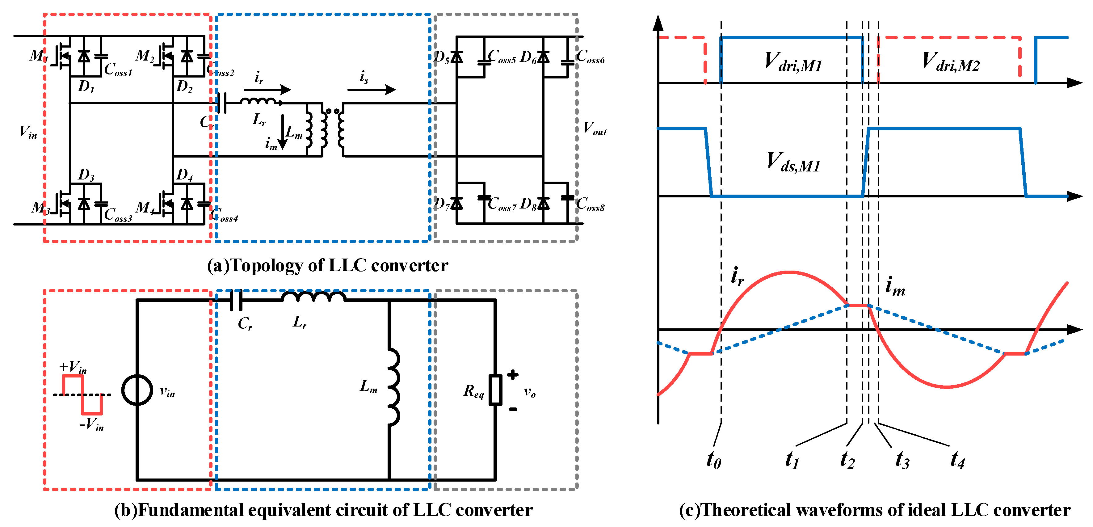
3.1. Operation Principle of the Ideal High-Frequency High Step-Up Ratio LLC Converter

The topology, fundamental equivalent circuit, and theoretical waveforms of the ideal LLC converter are shown in Figure 4. In Figure 4a, M1~M4, D1~D4 and Coss1~Coss8 represent the channels, body diodes and parasitic capacitor of the devices, respectively. Cr is the resonant capacitor, Lr is the resonant inductor, Lm is the magnetic inductor, and D5~D8 are the secondary-side rectifier diodes. The turn ratio of transformer is 1:n.
When the parasitic capacitance of the secondary side is very small and can be ignored, the operation of the LLC converter can be analyzed as being under ideal conditions. Figure 4c shows the theoretical waveforms of the ideal LLC converter, in which Vdri,M1 and Vdri,M2 are the drive signals of M1 and M2, Vds,M1 is the drain-source voltage of M1, and ir and im represent the resonant current and magnetic current, respectively. At t1, as the current drops to zero, the secondary diodes turn off naturally and achieve ZCS because of lower di/dt. Since the magnetic inductance of the ideal LLC converter can be considered to be large enough, im remains unchanged and ir remains the same as im. At t2, M1 and M4 are turned off and ir start to charge or discharge parasitic capacitors of devices. Because ir is always maintained at the peak value of im, the commutation of primary side can be completed in a very short time. Thus, the achievement of ZVS can be ensured at t4.
When the dead band and parasitic capacitance of secondary side are ignored, according to Figure 4b, the DC voltage gain G can be deduced from the fundamental equivalent circuit and can be expressed as:
G = V o u t V i n = 1 ( 1 + 1 k 1 k Ω 2 ) 2 + Q 2 ( Ω 1 Ω ) 2 ,
where Vout is the output voltage, Vin is the input voltage, k is the ratio of Lm to Lr, Ω is the normalized frequency, the ratio of switching frequency fs to resonant frequency fr and Q is the quality factor of the fundamental equivalent circuit, in which Req is the equivalent resistance of the secondary side of the transformer. The DC voltage gain of LLC has been shown in Figure 5. According to Figure 5, when fs > fr, there is no ZCS in the secondary side because of the high di/dt; however, when fs << fr, the LLC converter will operate in the capacitive zone and there is no ZVS. Therefore, the operation zone shown in Figure 5 is the best choice and fs < fr. Since the high-frequency ratio LLC converter operates as DCX, the larger k is preferred to resist the frequency disturbance because of its flatter DC voltage gain curve according to Figure 5b. It is obvious that the gain of the LLC converter changes by less than 10% with the changing of the load, even under the condition that fs = 0.9fr.

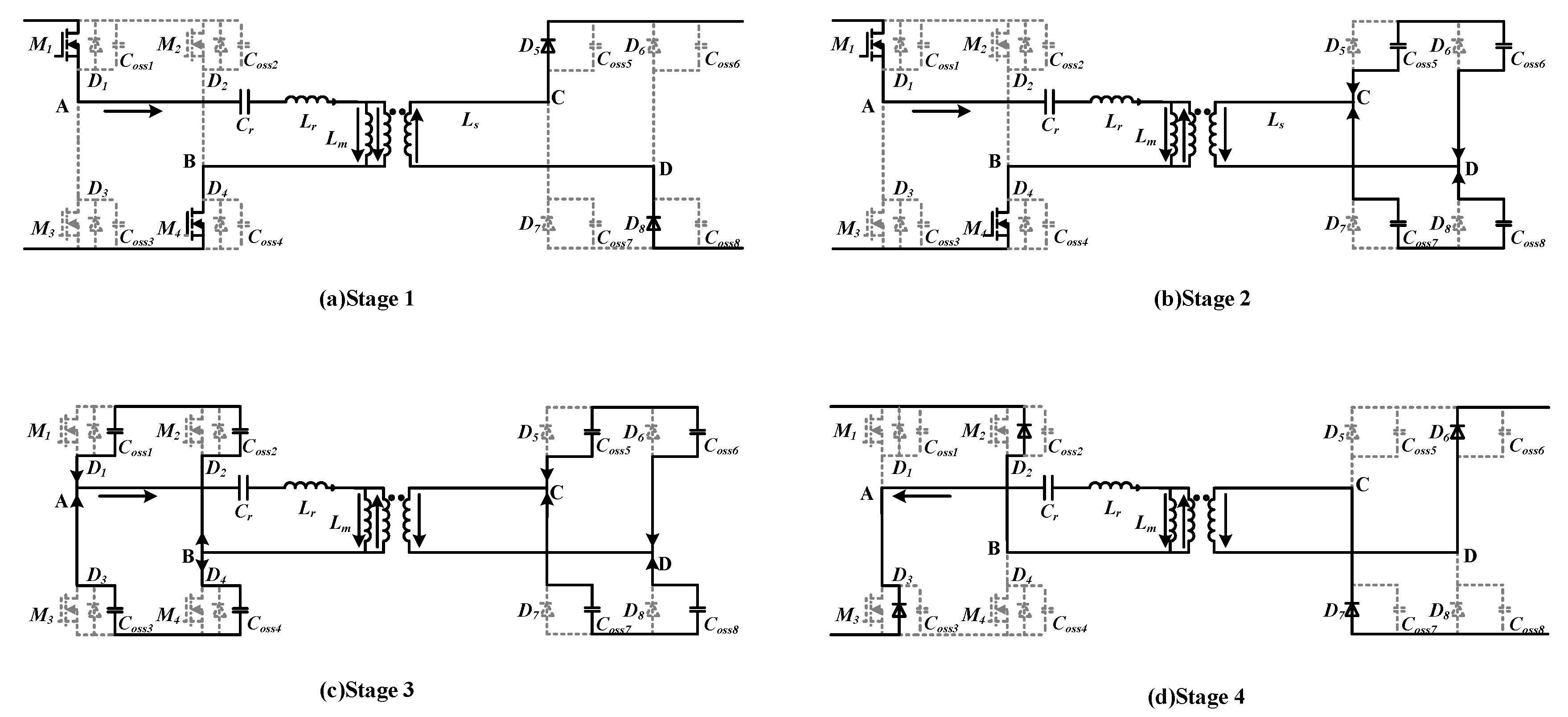
3.2. Analysis of the Operation Principle of the LLC Converter Considering Parasitic Parameters

In the practical application of the high-frequency LLC converter, the parasitic capacitor of the secondary diodes cannot be ignored. The topology of the LLC converter in consideration of the parasitic parameters is shown in Figure 6a. Coss5~Coss8 represent the junction capacitors of the rectifier diodes. The reference direction of ir, im and is are the same as the directions shown in Figure 6a.
In general, the LLC converter is designed in consideration of ideal conditions. Nevertheless, with the increase in the magnetic inductance of the LLC converter, the influence of the magnetic current becomes weaker, and the equivalent parasitic parameters of the secondary devices becomes much greater compared with LLC converters in traditional step-down applications. The parasitic parameters have a negative influence on the primary-side ZVS. The theoretical waveforms of the LLC converter considering parasitic parameters are shown in Figure 6c. Vdri,M1 and Vdri,M2 are the drive signals of M1 and M2, Vds,M1 is the drain-source voltage of M1, VD5 represents the voltage of the secondary rectifier diode D5, and ir and im represent the resonant current and magnetic current, respectively. In the first half cycle, the LLC converter can be divided into four states, as shown in Figure 7.
In Stage3, the parasitic capacitance of both sides participates in the resonance process, as shown in Figure 7c. The equivalent circuit of Stage3 between t2 and t3 is shown in Figure 6b. Coss,p and Coss,s represent the parasitic capacitance of the primary and secondary devices, respectively. According to the equivalent circuit, the secondary-side parasitic capacitance was changed by n2, and the influence on the resonance process was changed as well. Additionally, with the extensive use of SiC devices, the switching frequency of the LLC converters is continuously improved, and the loss increase caused by the loss of ZVS is more serious.
Since the waveform of the LLC converter is completely symmetrical in every half cycle, only the former half cycle is analyzed.
Stage 1 (t0~t1): As shown in Figure 7a, both M1/M4 and D5/D8 are conductive. The voltage of Lm is clamped by the output voltage, and the im increases linearly. Because the resonant elements Lr and Cr form a band-pass filter, only the current near the resonant frequency is able to pass through the resonant network. Therefore, ir varies as a resonant frequency sinusoidal curve.
Stage 2 (t1~t2): As shown in Figure 7b, M1 and M4 are still conductive, while D5 and D8 are naturally turned off, because the current drops to zero with a low di/dt. Thus, ZCS is achieved on the secondary side. Then, the secondary-side parasitic capacitors Coss5~Coss8 are introduced into the resonant network. A higher frequency resonance occurs in both VD5 and ir. In this stage, ir fluctuates near im.
Stage 3 (t2~t3): As shown in Figure 7c, M1 and M4 are turned off and ir starts to charge or discharge the parasitic capacitors Coss1~Coss4. In this stage, both Coss1~Coss4 and Coss5~Coss8 are involved in the resonance process. This stage is very important, because the resonance process has a great influence on the primary-side ZVS. In this stage, according to the Kirchhoff voltage laws (KVL), ir should meet:
{ u c q + u c r + L r d i r d t + L m d i m d t = 0 L m d i m d t = u c d
Furthermore,
{ i r = C q d u c q d t = C r d u c r d t i m = i r C d d u c d d t
where Cq, Cr and Cd are capacitances of Coss1~Coss4, the resonant capacitor and Coss5~Coss8, respectively. Ucq, ucr and ucd are the voltage of corresponding capacitor, and ir and im represent the current of the resonant inductor Lr and magnetic inductor Lm. The initial values are the final values of Stage 2.
Stage 4 (t3~t4): As shown in Figure 7d, primary-side commutation is completed and D2 and D3 are turned on naturally. At the same time, D6 and D7 are turned on as well. The voltage of Lm is clamped by the output voltage, and the im increases linearly. ir varies as a resonant frequency sinusoidal curve. At t4, M2 and M3 are turned on, and the ZVS is achieved.
Obviously, with the addition of secondary-side parasitic capacitors, the resonance process in Stage 3 is changed dramatically, according to Equations (2) and (3). This change may mean that the ZVS cannot be achieved. Usually, the achievement of ZVS needs to meet:
{ i r ( t ) 0 0 T d e a d i r ( t ) d t 2 C q V i n
where Tdead is the dead band of the converter. In Equation (4), the first condition ensures that the voltage of the primary side devices can achieve ZVS, and the second condition ensures that ir can provide sufficient charge to achieve ZVS in the dead band. Therefore, ir(t) is very important for the realization of primary-side ZVS. According to Equations (2) and (3), the ir(t) in Stage 3 can be plotted by MATLAB. Then, the influence of secondary parasitic capacitance on ZVS can be obtained according to Figure 8. Figure 8 presents the change of Vds,M1 during the transient with different Cd and Lm or Lr. When Cd = 0, the equivalent circuit becomes the circuit of the ideal LLC converter and Vds,M1 change linearly.
As shown in Figure 8, with the increase of Cd, ir is shared by the parasitic capacitors of the secondary side, which increases the time required to fully charge the primary-side capacitors. To ensure that ZVS can be achieved, the dead band must be longer than the time needed to charge Coss1 and Coss4. Furthermore, since the switch turns off after ir is equal to im, ir(t2) = im(t2) is assumed.
According to Figure 8a, the Lm influences the resonance process and ZVS. It is obvious that the smaller Lm is, the larger initial ir(t2) is and the shorter the time needed to achieve ZVS under the same parasitic parameter conditions. However, smaller Lm will lead to larger conduction loss and switching loss. Therefore, a careful tradeoff has to be made.
Additionally, according to Figure 8b, Lr also influences ZVS. The change of Lr leads to the change of resonant frequency and impedance in the resonance process. Then, the time to achieve ZVS is changed. It is obvious that the larger the Lr is, the more serious the influence of parasitic capacitance on the ZVS will be.
The above analysis shows that when parasitic capacitance can be extracted, to achieve ZVS, Lm, Lr and Tdead should be carefully designed in the high-frequency LLC converter.
In the traditional design method for LLC converters, to achieve ZVS, Lm is usually limited by:
L m n V o T d e a d 8 V i n C q f s
However, Equation (5) ignores the secondary-side parasitic capacitors and resonance process in the dead band. According to the above analysis, there are two ways of ensuring the realization of ZVS via careful parameter design. The first is that ir is always larger than zero. This means that ZVS can be achieved only by adjusting the dead band (of course, the dead band must be within acceptable limits). The second is that the charge or discharge of primary-side parasitic capacitors can be completed before ir drops to zero. To achieve ZVS, generally the Lm is selected as a small value compared to the theoretical value calculated by Equation (5). However, Lm is an important parameter in high-frequency LLC converters, because it not only affects the realization of soft switching, but also the power loss of the converter. In the LLC converter, the resonant current ir, magnetic current im, primary-side current of transformer ip and secondary-side current of transformer is can be derived as:
{ i r ( t ) = I r sin ( 2 π f s t φ ) i m ( t ) = { n V o u t t L m I m 0 t 1 2 f s n V o u t ( t 1 2 f s ) L m + I m 1 2 f s < t 1 f s i p ( t ) = i r ( t ) i m ( t ) i s ( t ) = n i p ( t )
{ I m = n V o u t 4 L m f s I r = ( π P 2 n V o u t ) 2 + I m 2 φ = arcsin ( I m I r )
Thus, the conduction loss and switching loss of LLC can be calculated, and the relationship between the total loss Ploss and Lm is shown in Figure 9. There is an obvious demarcation point in Figure 9, namely, Lm.min. When Lm is smaller than Lm.min, the Ploss increases rapidly with the decrease of Lm, no matter at light load condition or at heavy load condition, which will lead to a lower efficiency in the full load range. Therefore, a new method to suppress the influence of parasitic parameters in the LLC converter without efficiency loss is very important to improve the efficiency of the PV system.

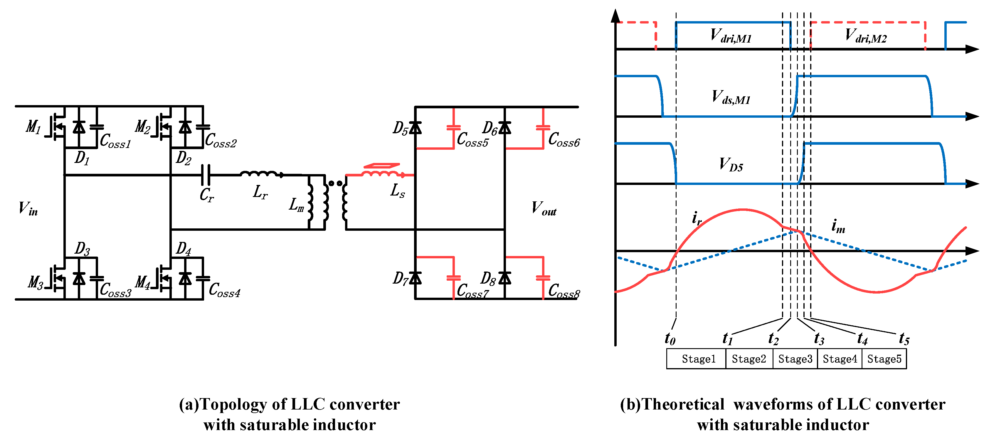
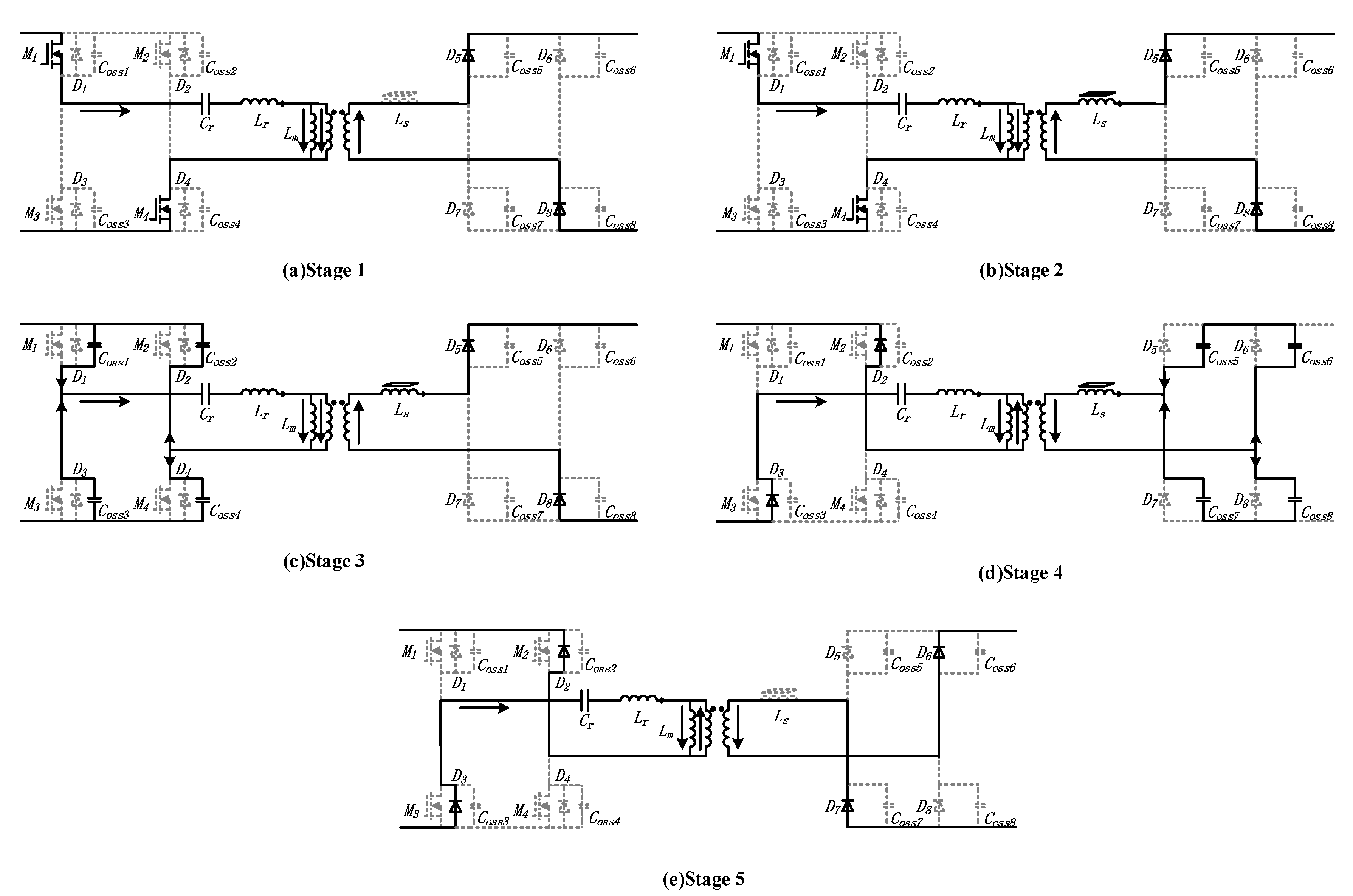
4. Suppression Method of the Influence of Parasitic Parameters Based on the Saturable Inductor

In the PV system, LLC converters based on SiC devices have a higher switching frequency, which can further improve the system efficiency and the power density of the system. However, parasitic parameters lead to the loss of ZVS, the increase in power loss, and the deterioration of EMI characteristics at high frequencies. Although the methodological analysis above is able to suppress the influence of secondary parasitic parameters by reducing the Lm, the increase in power loss is still inevitable. To ensure the implementation of ZVS and improve the efficiency of the LLC converter, a structure for an LLC converter with a saturable inductor, as shown in Figure 10a, is proposed. In addition, its theoretical waveforms are shown in Figure 10b.
In Figure 10a, Ls is the initial inductance of the saturable inductor, and Ic is the current when Ls becomes saturated. The Ls is added to the secondary side. Since the Ic is very small, the Ls is saturated for most of the time in a cycle, and the circuit structure is the same as that of the traditional LLC converter. When the secondary current is is near to zero, the Ls gradually withdraws from the saturated state, and is added into the secondary circuit as an inductor. Therefore, Ls blocks the parasitic capacitance of the secondary side to participate in the resonance process and ensures the achievement of ZVS of the primary side. According to Figure 10b, the operation of the LLC converter with the saturable inductor can be divided into five stages.

4.1. Analysis of the Operation Principle of the LLC Converter with the Saturable Inductor

The five stages of the LLC converter with the saturable inductor are shown in Figure 11.
Stage 1 (t0~t1): As shown in Figure 11a, both M1/M4 and D5/D8 are conductive. The voltage of Lm is clamped by the output voltage, and the im increases linearly. Because the resonant elements Lr and Cr form a band-pass filter, only the current near the resonant frequency is able to pass through the resonant network. Therefore, ir varies as a resonant frequency sinusoidal curve. In this stage, according to KVL:
{ V i n u c r L r C r d 2 u c r d t L m d i m d t = 0 L m d i m d t = V o
Stage 2 (t1~t2): As shown in Figure 11b, M1 and M4 are still conductive, and |is| < Ic. Thus, the Ls participates in the operation of the LLC converter and D5 and D8 remain conductive. Therefore, ir decreases slowly and linearly. In this stage, according to KVL:
{ V i n u c r L r d i r d t L m d i m d t = 0 L m d i m d t = V o + L s d i s d t
According to Kirchhoff current laws (KCL):
i r = i m + i s = C r d u c r d t
Stage 3 (t2~t3): As shown in Figure 11c, M1 and M4 are still conductive, while D5 and D8 are still conductive because of the presence of Ls. Then, ir starts to charge or discharge parasitic capacitors Coss1~Coss4. At this stage, ir decreases slowly and Coss1 and Coss4 are fully charged in a short time. Therefore, according to KVL, ir meet:
{ u c q + u c r + L r d i r d t + L m d i m d t = 0 L m d i m d t = V o + L s d i s d t
According to KCL and voltage-current relationship (VCR):
i r = i m + i s = C r d u c r d t = C q d u c q d t
Stage 4 (t3~t4): As shown in Figure 11d, D2 and D3 naturally become conductive, because Coss2 and Coss3 were fully discharged in Stage 3. Then, is drops to zero, D5 and D8 are turned off and ZCS can be achieved because of lower di/dt. After that, Coss5~Coss8 participate in the resonance process and are charged or discharged. In this stage, according to KVL:
{ V i n u c r L r d i r d t L m d i m d t = 0 L m d i m d t = u c d + L s d i s d t
According to KCL and VCR:
i r = i m + i s = C r d u c r d t = C q d u c q d t i s = C d d u c d d t
Stage 5 (t4~t5): As shown in Figure 11e, both D2/D3 and D6/D7 are conductive and Ls becomes saturated. The voltage of Lm is clamped by the output voltage, and the im decreases linearly and ir varies as a resonant frequency sinusoidal curve. At t5, the M2 and M3 are turned on, and primary side ZVS is achieved. In this stage, according to Figure 11e:
{ V i n + u c r + L r C r d 2 u c r d t + L m d i m d t = 0 L m d i m d t + V o = 0
Besides, some s-domain analysis has been shown in the Appendix B.

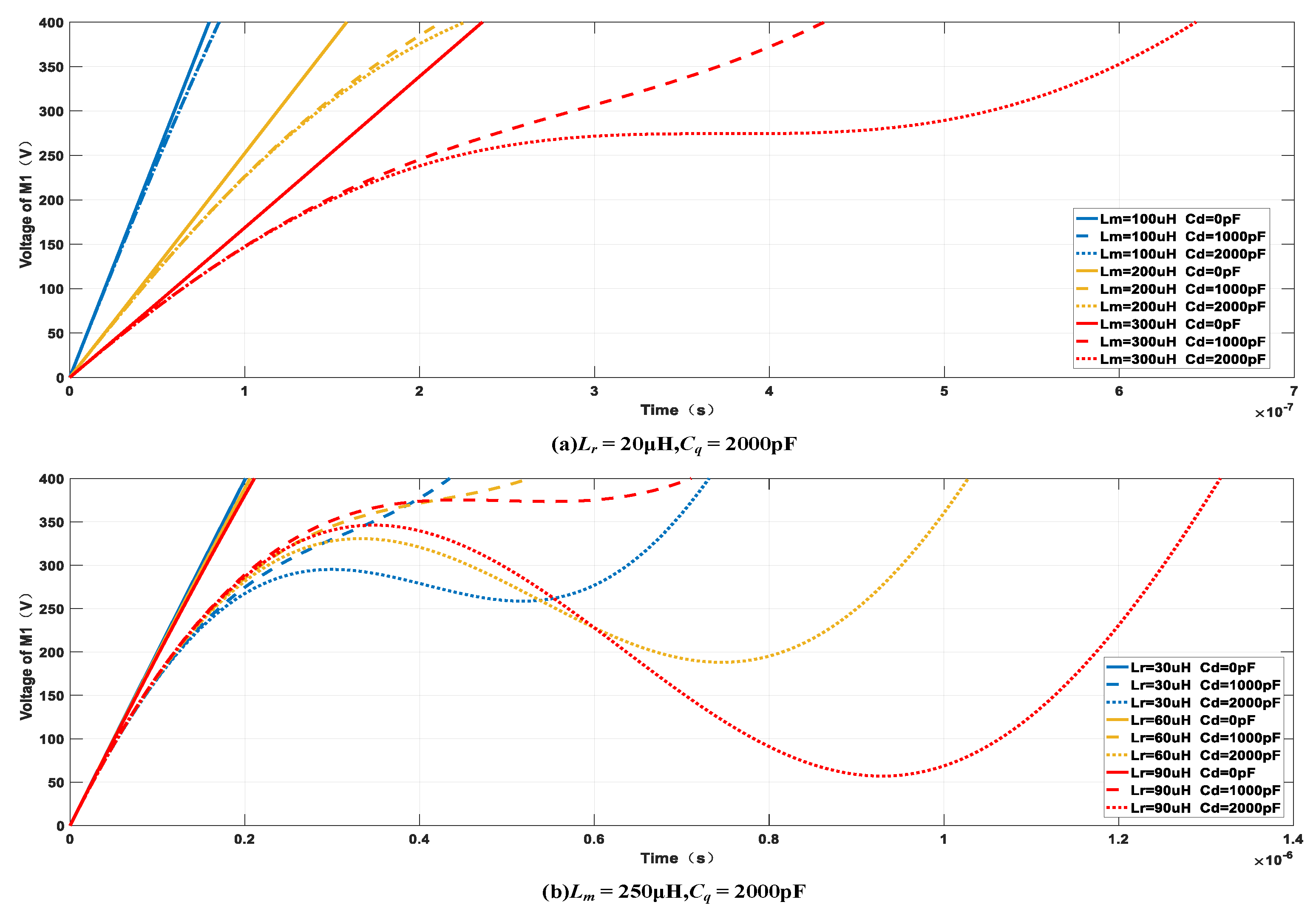
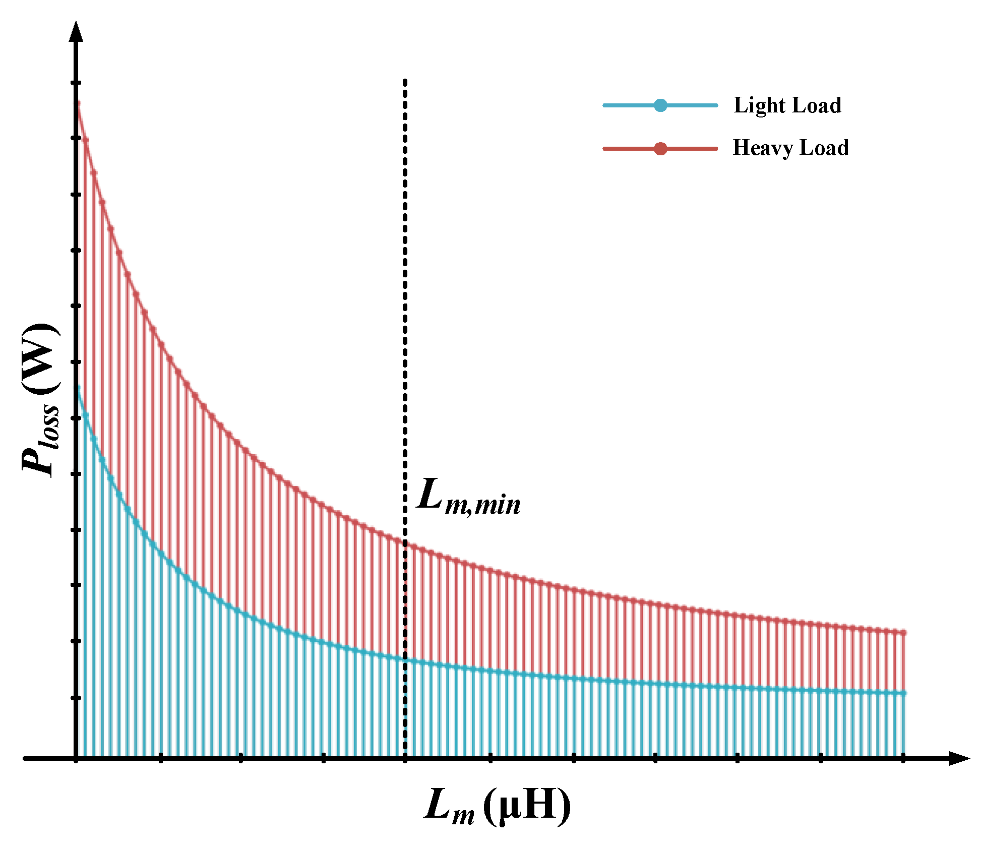
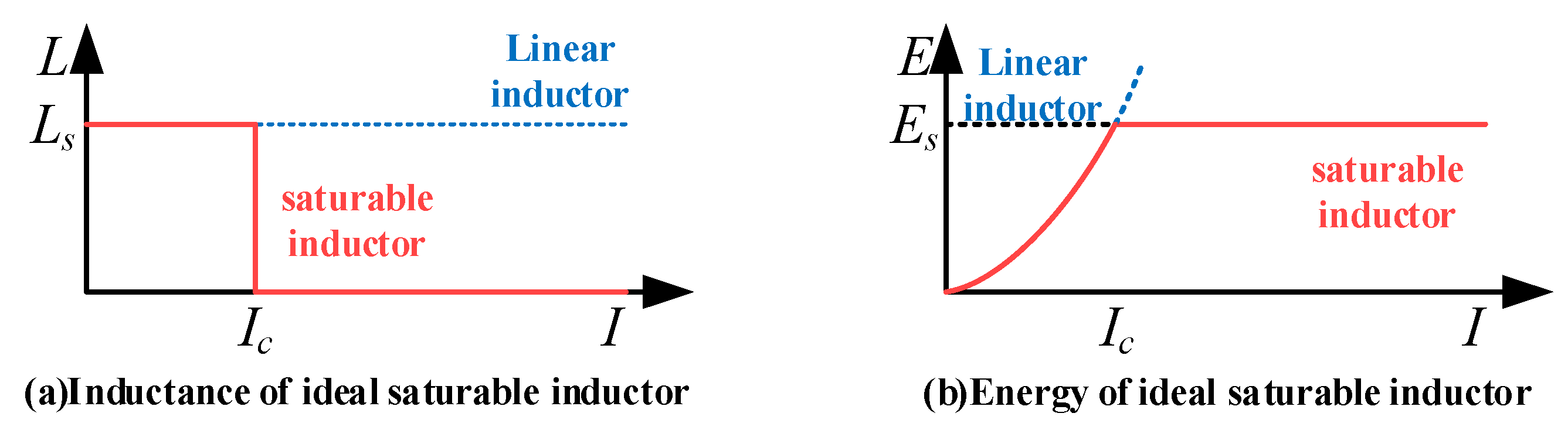
4.2. Analysis and Design of the Saturable Inductor

The inductance and energy storage of the ideal saturable inductor are shown in Figure 12.
In Stage 2 and Stage 3, Ls maintains is greater than zero, which causes the rectifier diodes to be continuously conductive. At these two stages, secondary-side parasitic capacitance will not participate in the operation of the circuit. In Stage 3, Ls causes the ir to remain basically unchanged, which leads to a shorter time for the primary side until commutation. Then, the secondary side voltage of the transformer can be approximated as:
V s V i n + V c + L r d i r ( t ) d t
where the Vc is the peak value of the resonant capacitor voltage, so the is(t) can be expressed as:
i s ( t ) = I c V o V s L s t
To ensure the completion of primary-side commutation, is should always be greater than zero at t3, that is:
I c L s ( V o V s ) ( t 3 t 1 )
In Stage 4, the Ls causes the is to be less than zero. After the secondary diodes are turned off and ZCS is achieved, the parasitic capacitors participate in the resonance process. At t4, is decreases to −Ic and D6 and D7 become conductive. Then, the Ls becomes saturated and no longer participates in the operation of the circuit. In Stage 5, the resonant current ir(t) can be expressed as:
i r ( t ) I m I c + V o + V c V i n L r t
where Im is the peak value of im. To ensure that the primary-side body diode is conductive in these two stages, the ir(t) must be greater than zero; therefore,
I c I m + V o + V c V i n L r ( t 5 t 4 )
According to the constraints of (19) and (21), the values of Ic and Ls for the saturable inductor can be designed.

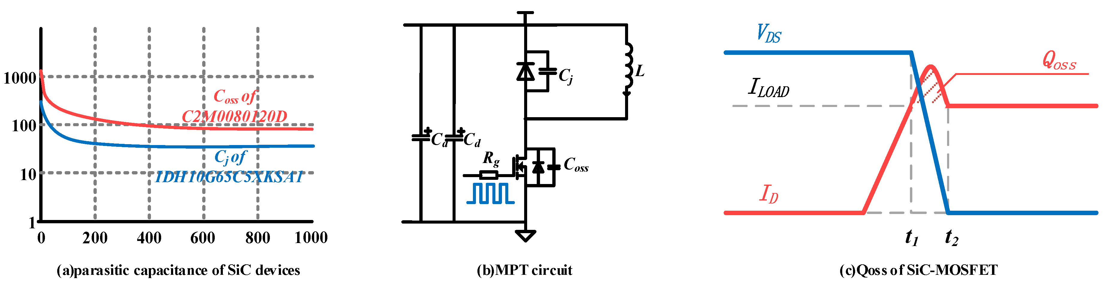
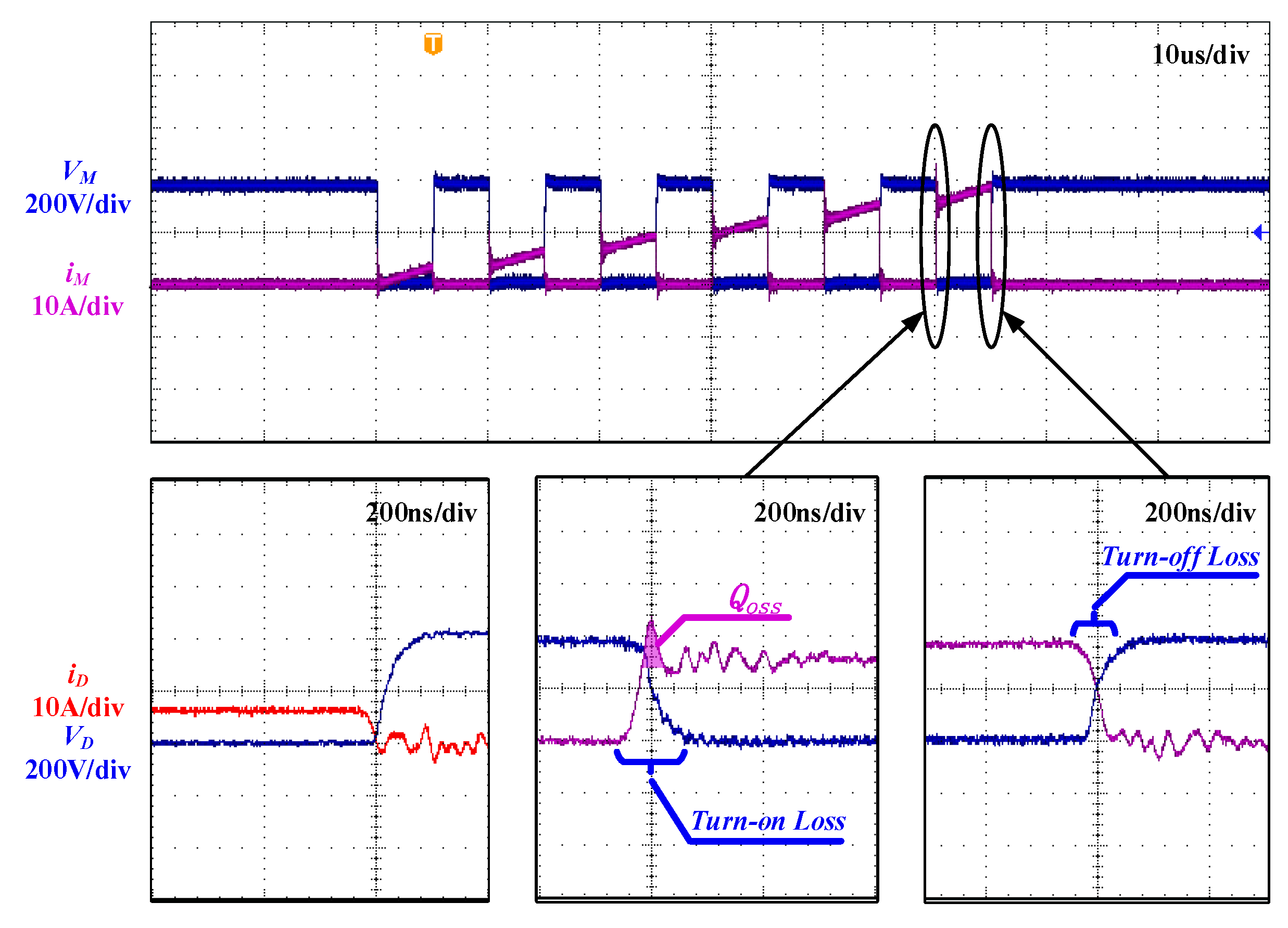
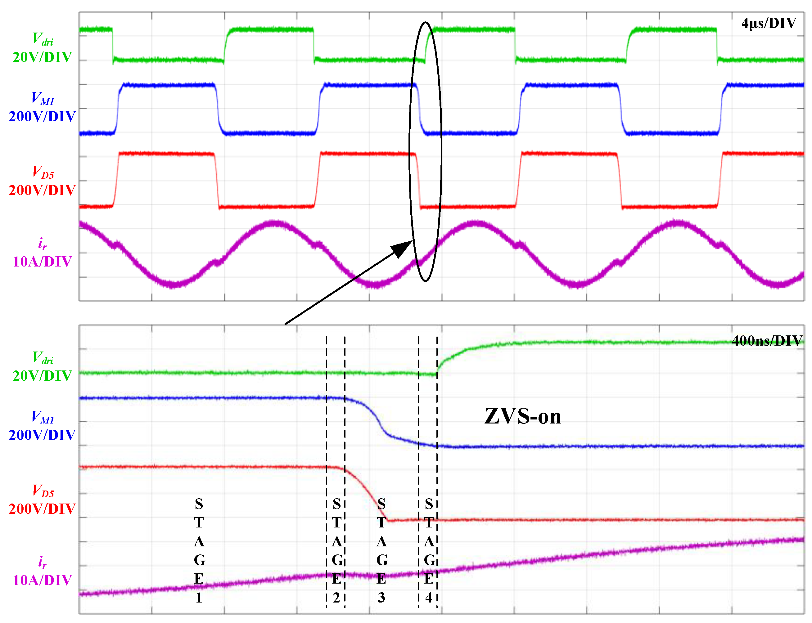
5. Experimental Verification and Analysis

To verify the influence of parasitic parameters on ZVS, as well as to validate the two suppression methods proposed in this paper, a 2000 W down-scale prototype is built.
Since the system is based on SiC devices, the driving circuit and protection constitute an important technology. In comparison with Si-MOSFET, SiC-MOSEFET has some significant differences in terms of its characteristics, due to its different material and structure. SiC-MOSEFET has the advantages of low on-state resistance and fast switching speed. However, due to the low gate threshold voltage, it is more likely to suffer from interference and erroneous conduction. Therefore, the driving circuit of SiC-MOSFET cannot be simply replaced by that of Si-MOSFET.
In the LLC converter, SiC devices are mainly used as full-bridge switching devices on the primary side. Usually the switching on and off of SiC devices is affected by their output capacitance under soft-switching conditions, and the crosstalk problem is not serious. However, because the switching speed of SiC devices is very fast and the transient dv/dt is very large, once the ZVS has been lost, the crosstalk problem becomes very serious. Subsequently, the increase in gate voltage caused by crosstalk will be threatening to SiC-MOSFET during this period. Therefore, effective driving and protection circuits are also the focus of the driving design of the SiC devices.
CREE, ROHM and other companies have successively introduced commercial SiC device driving circuits, but few of these circuits involve solutions to driving protection problems. In this paper, C2M0080120D is used as the primary side switch in the experiment. To meet the high reliability requirement of the PV system, short-circuit protection is considered in the design of the driving circuit, as shown in Figure 13. SiC devices are driven by a 24 V isolated power supply, and a BROADCOM ACPL-339J-000E optocoupler driver chip is used to achieve isolation and protection. This chip provides a user-setup desaturation protection circuit scheme, which is able to provide effective protection for the devices and improve system reliability when a short-circuit occurs. In the driving circuit, the gate parallel resistor and capacitor of SiC-MOSFET are able to reduce the influence of crosstalk. In the short-circuit protection circuit, Cblank and ZDESET are designed according to the actual needs, whereby Cblank determines the allowable blank time of driving protection and ZDESET determines the corresponding current value of protection. When short-circuit protection is triggered, VGMOS will increase to a high level. The soft turn-off time is determined by the series resistance of Q3 and the input capacitance Ciss of SiC-MOSFET.
As shown in Figure 14a, the parasitic capacitance of the SiC-MOSFET and SiC diodes is usually nonlinear. Therefore, the time-related equivalent parasitic capacitance Coss(tr) is very important. Generally, the MPT circuit shown in Figure 14b can be used to measure the equivalent parasitic capacitance. Figure 14c shows the hard switching process of the SiC MOSFET. VDS is the drain-source voltage of the device, ILOAD is the load current, ID is the drain current of the device, and Qoss is the charge caused by Coss. According to the characteristics of the capacitor, the Coss(tr) can be calculated as
C o s s ( t r ) = t 1 t 2 i D ( t ) d t V D S
where iD(t) is the expression of drain current between t1 and t2.
The waveforms of the MPT are shown in Figure 15. VM is the drain-source voltage, iM is the drain current, iD is the current of the diode and VD is the voltage of the diode. The test voltage is 400 V, and the final current is 20 A. According to the results of MPT, the driving circuit was verified. The Qoss was calculated, and the Coss(tr) obtained by (21) was 1.6 nF. Additionally, the switching loss of SiC-MOSFET under hard-switching conditions can be calculated.
According to the analysis above, in consideration of parasitic parameters, the parasitic capacitance of primary- and secondary-side devices is very important for the parameter design of high-frequency LLC converters. However, the parasitic capacitance is not a fixed value. It is related to the voltage of the device. Generally, the values of parasitic capacitance are replaced by time-related equivalent capacitance. The equivalent capacitances of C2M0080120D and IDH10G65C5XKSA1, which are used in the experiment, are shown in Table 2. The parameters of the experimental prototype are also listed in Table 2.
Figure 16 shows the waveform of the LLC converter using the traditional magnetic inductance limitation. According to Equation (5), the maximum inductance value of Lm is 500 μH when the dead band is extended from 500 ns to 700 ns, in accordance with [31]. To ensure that ZVS can be achieved, considering a margin of 1.5 times, the 300 μH is selected as the experimental inductance in the experiment. In Figure 16, ir is the resonant current, VM1 is the voltage of M1, VD5 is the voltage of D5, and Vdri is the driving signal of M1. Although the margin is considered in the design, the ZVS still cannot be realized under full-load conditions. Hard switching increases the interference in the driving signals and reduces the efficiency of the converter. In addition, since there is some interference in the driving signals, this experimental method cannot be used in the actual system. In Figure 16, Stage 1~3 correspond to the stages in the theoretical analysis. In Stage 1, ir is part of a sinusoidal waveform and M1 has been turned off. At the beginning of Stage 2, ir begins to oscillate instead of being maintained near the magnetic current because of the participation of parasitic capacitors of the secondary-side diodes. Since the fs is only slightly smaller than fr, this stage is very short. At the beginning of Stage 3, the parasitic parameters of the primary- and secondary-side devices participate in a resonance process together until the dead band ends or the ZVS has been achieved. It is noteworthy that the secondary diodes become conductive before the ZVS is achieved. Then, ir begins to transmit power to the load, causing the realization of ZVS to become impossible. Therefore, even though the dead band is extended, the ZVS cannot be achieved, as shown in Figure 16.
Figure 17 shows the waveform of the LLC converter, where the magnetic inductance is reduced according to [31,35]. The parasitic capacitance is measured by MPT, and 80 μH is finally selected as the experimental inductance according to a simulation. In Figure 17, it can be seen that ZVS can be achieved under full-load conditions. Additionally, there is no interference in the driving signal. However, the magnetic current clearly increases because of the reduction of the magnetic inductance, which leads to the increase of conduction loss and switching loss. In Figure 17, Stage 1~4 correspond to the stages in the theoretical analysis. Stage 1 and Stage 2 are similar to the stages in Figure 16. At the beginning of Stage 3, the parasitic parameters of the primary- and secondary-side devices also participate in the resonance process together until the dead band ends or ZVS has been achieved. However, since the magnetic inductance is reduced and the magnetic current is increased, the primary-and secondary-side commutation finish almost simultaneously. Then the load will be supported by source instead of by resonant inductor. Therefore, in Stage 4, the primary side ZVS is achieved.
Figure 18 shows the experimental waveform of the LLC converter with the saturable inductor on the secondary side. 300 μH is selected as the magnetic inductance for comparison. It can be seen that ZVS can be realized under full-load conditions. Additionally, there is no interference in the driving signal. Since the magnetic current has hardly increased, the loss is obviously reduced compared with the method of reducing the magnetic inductance. In Figure 18, Stage 1~5 correspond to the stage in theoretical analysis. In Stage 1, ir is part of sinusoidal waveform and M1 has been turned off. As the |ir| decreases, the saturated inductor gradually exits out of the saturated state, and then the Stage 2 begins. Thereafter, the ir varies linearly. At the beginning of state 3, the primary device begins to commutate, which is different from the two experiments mentioned above. Since the saturable inductor keeps the secondary current constantly below 0, the parasitic capacitance of the secondary-side diodes no longer p in this stage. Then the problem of the secondary side completing the commutation before the primary side can be avoided. At the beginning of Stage 4, the primary side commutation is completed and ZVS-on is realized. When the current is exceeds 0, the secondary diodes begin to commutate. If the primary switch is not fully turned on and the secondary commutation is finished, the secondary diodes enter Stage 5. It is obvious the resonant current of this experiment is much lower than that shown in Figure 17. This means that higher efficiency can be obtained.
Figure 19 shows the efficiency curves and loss breakdowns of three experiments under full load conditions. It is obvious that the proposed method is able to achieve the highest efficiency across the full load range compared with the others. The full load efficiency of the proposed method is able to achieve 98.6%. Although the efficiency of the experimental parameters designed by traditional method with the extended dead band is only slightly lower than the proposed method, it is still not suitable for practical application due to its terrible driver conditions, as shown in Figure 16. The converter with reduced magnetic inductance is clearly able to achieve ZVS. However, according to the theoretical analysis shown in Appendix A, from the point of view of power loss, the loss of the primary-side devices is significantly increased. Compared with the former, the method based on the saturable inductor is able to reduce the conduction loss by 56.74% and the switching loss by 73%. Then, the full-load efficiency can be increased by 0.7%. Obviously, the suppression method based on the saturable inductor is better.

6. Conclusions

This paper presents the architecture of a high frequency link 35 kV PV system and studies the influence of the parasitic parameters of the high-frequency high-voltage isolated DC–DC converter. This paper reveals how the parasitic parameters affect the realization of ZVS of the LLC converter in high-frequency situations, and proposes a method for suppressing the influences of parasitic parameters and promoting the realization of ZVS. The method effectively prevents parasitic elements of the secondary side from participating in the resonance of the primary side by adding a saturable inductor on the secondary side to ensure that ZVS can be achieved.
This paper has some advantages compared to the existing research,
  • The influence of the parasitic parameters of SiC devices on the high-frequency LLC converter is analyzed step by step, which is more accurate.
  • The mechanism of influence of the parasitic parameters on the resonance process is discussed systematically. This paper reveals how different parameters are able to affect the resonance process with respect to parasitic parameters.
  • Compared to the extended dead band, the proposed suppression method is able to cause ZVS to be realized and to eliminate the driving interference.
  • Compared to the reduced magnetic inductance, the proposed suppression method can significantly decrease the power loss caused by magnetic inductance. The conduction loss can be reduced by 56.74% and the switching loss by 73%. The efficiency can be improved by 0.7%.
Compared with the conventional method, which involves reducing magnetic inductance, the proposed method does not need to reduce the magnetic inductance, and this is beneficial for reducing the magnetic current of the transformer and improving the efficiency of the LLC converter. The experimental verification shows that the theoretical analysis is consistent with the actual situation. The proposed parasitic parameter suppression method is able to significantly improve the efficiency of the LLC converter. Furthermore, the proposed method is able to improve the efficiency and performance of the MVAC PV system.

Author Contributions

Conceptualization, F.S. and R.L.; methodology, F.S. and R.L.; validation, F.S. and R.L.; formal analysis, F.S.; writing—original draft preparation, F.S.; writing—review and editing, R.L. and X.C.; project administration, R.L., X.C. and H.X.

Funding

This research was funded by Key Area R&D Program of Guangdong Province, grant number 2019B010127001.

Conflicts of Interest

The authors declare no conflict of interest.

Appendix A

On the basis Equations (6) and (7), the resonant current ir, magnetic current im and secondary side current of transformer is can be calculated. Since the drain-source voltage Vds and conduction resistance Rds(on) of the device are known, the conduction loss and switching loss of the devices can therefore be calculated.
Usually, the conduction loss Pc, turn-on loss Pon and turn-off loss Poff can be calculated by (A1)–(A3), as follows:
P c = I d r m s R d s ( o n )
P o n = f s 0 t r ( V d s V d s t r t ) i d t r t d t
P o f f = f s 0 t f ( I D i d t f t ) V d s t f t d t
where Idrms is the RMS value of the drain current, tr is the rise time of the current, tf is the fall time of the current, fs is the switching current and ID is the conduction drain current.
Furthermore, loss due to magnetic components is also important. During the design process, it is possible to obtain the maximum magnetic flux density Bm. Then, on the basis of the datasheet of the selected core, it is possible to calculate the core loss Pcore. Since the parameters of the winding are known, the DC equivalent resistance and AC equivalent resistance can be calculated, as well. Finally, the loss due to magnetic components Pm can be obtained.
Therefore, it is possible to accurately calculate the main losses of the converter by theoretical analysis.
In Figure A1, the s-domain equivalent circuit of each stage of the LLC converter with a saturable inductor is shown. Then, the accurate expression of each stage in the s-domain can be written and derived as follows:

Appendix B

Figure A1. S-domain equivalent circuit of each stage of the LLC converter with a saturable inductor.
Energies 12 03743 g0a1
i r ( s ) = C r L r i r ( t 0 ) s + C r [ V i n V o + v c ( t 0 ) ] C r L r s 2 + 1
i r ( s ) = c 1 s + c 0 c 3 s 2 + c 2 { c 0 = L s C r V i n + L s C r v c ( t 1 ) L s C r V o V o L m C r c 1 = L s C r i r ( t 1 ) L r + L s C r i s ( t 1 ) L s + L s C r i m ( t 1 ) L m + L s C r i m ( t 1 ) L s + L s C r i s ( t 1 ) L m c 2 = L s c 3 = L s C r ( L r + L m + L s )
i r ( s ) = d 1 s + d 0 d 3 s 2 + d 2 { d 0 = L s C r C q V i n + L s C r C q v c ( t 2 ) L s C r C q V o L m C r C q V o d 1 = L s C r C q i r ( t 2 ) L r + L s C r C q i s ( t 2 ) L m + L s C r C q i m ( t 2 ) L m + L s 2 C r C q i m ( t 2 ) + L s 2 C r C q i s ( t 2 ) d 2 = L s ( C r + C q ) d 3 = L s C r C q ( L r + L m + L s )
i r ( s ) = e 4 s 4 + e 3 s 3 + e 2 s 2 + e 1 s + e 0 e 7 s 5 + e 6 s 3 + e 5 s e 0 = i m ( t 3 ) C r e 1 = C r C d [ v c ( t 3 ) V o V i n ] e 2 = C r C d [ i r ( t 3 ) L r + i s ( t 3 ) L s + i s ( t 3 ) L m + i m ( t 3 ) L s ] e 3 = L s C r C d 2 [ v c ( t 3 ) V o V i n ] L m C r C d 2 V o e 4 = L s C r C d 2 [ i r ( t 3 ) L r + i s ( t 3 ) L s + i s ( t 3 ) L m + i m ( t 3 ) L m + i m ( t 3 ) L s ] e 5 = C r + C d e 6 = L s C d 2 + L r C r C d + L m C r C d + 2 L s C r C d e 7 = L s C r C d 2 [ i r ( t 3 ) + L m + L s ]
i r ( s ) = C r L r i r ( t 4 ) s + C r [ V o + v c ( t 4 ) V i n ] C r L r s 2 + 1
where Cq and Cd are the capacitances of Coss1~Coss4 and Coss5~Coss8, respectively; Vo is the equivalent voltage of Vout converted to the primary side of transformer; and ir(tn), vc(tn) and im(tn) represent the values of ir, vc and im at tn(n = 0, 1, 2, 3). Ls is the inductance of the saturable inductor, Lr is the resonant inductance, Lm is the magnetic inductance and Cr is the resonant capacitance.

Appendix C

The symbols used in this paper are shown in Table A1.
Table A1. Symbols used in the paper.
SymbolDescription
VbusDC bus voltage
VgridGrid voltage
PPower
NCHBNumber of CHB in one phase
LgInductance of grid side
vdc(ki) (k = a, b, c and i = 1, 2, …, n)DC side voltage of unit(i) in phase k
pkiPower reference of CHB of unit(i) in phase k
vdc* DC side voltage reference
vd, vd-, vq, vq-D-axis and q-axis components of positive and negative sequence of grid voltage
id, id-, iq, iq-D-axis and q-axis components of positive and negative sequence of grid current
va,vb,vcGrid voltage
ia,ib,icGrid current
θPhase angle of the grid
vabc*Three phase voltage reference
M1~M4Channels of MOSFETs
D1~D4Body diodes of MOSFETs
D5~D8Secondary side rectifier diodes
Coss1~Coss8Parasitic capacitor of MOSFETs
LrResonant inductance
LmMagnetic inductance
CrResonant capacitance
LsInductance of the saturable inductor
nTurn ratio of transformer
Vdri,M1, Vdri,M2Drive signals of M1 and M2
Vds,M1Drain-source voltage of M1
VD5Voltage of secondary rectifier diode
irResonant current
imMagnetic current
GDC voltage gain
VoutOutput voltage of LLC
VinInput voltage of LLC
kRatio of Lm to Lr
ΩNormalized frequency
fsSwitching frequency
frResonant frequency
QQuality factor
Coss5~Coss8Junction capacitors of rectifier diodes
Coss,p, Coss,sParasitic capacitance of primary and secondary devices
Cq, Cr, CdCapacitance of Coss1~Coss4, resonant capacitor and Coss5~Coss8
ucq, ucr, ucdVoltage of Cq, Cr, Cd
TdeadDead band of the converter
VoEquivalent output voltage
ipPrimary side current of transformer
isSecondary side current of transformer
ImThe amplitude of magnetic current
IrThe amplitude of resonant current
φPhase of resonant current
PlossPower loss of LLC
Lm.minDemarcation point magnetic inductance
LsInitial inductance of the saturable inductor
IcValue of current when Ls becomes saturated
VsSecondary side voltage of transformer
VcPeak value of the resonant capacitor voltage
Coss(tr)Time related equivalent parasitic capacitance
VDSDrain-source voltage
ILOADLoad current
IDDrain current
QossCharge caused by Coss
PcConduction loss
PonTurn-on loss
PoffTurn-off loss
IdrmsRMS value of the drain current
trRise time of current
tfFall time of current
BmMaximum magnetic flux density
PcoreCore loss
PmLoss of magnetic components

References

  1. Wang, Y.; Lin, X.; Pedram, M. A near-optimal model-based control algorithm for households equipped with residential photovoltaic power generation and energy storage systems. IEEE Trans. Sustain. Energy 2016, 7, 77–86. [Google Scholar] [CrossRef]
  2. Xie, F.; Luo, Z.; Qiu, D.; Zhang, B.; Chen, Y.; Huang, L. Study on a Simplified Structure of a Two-Stage Grid-Connected Photovoltaic System for Parameter Design Optimization. Energies 2019, 12, 2193. [Google Scholar] [CrossRef]
  3. Van Sark, W. Photovoltaic System Design and Performance. Energies 2019, 12, 1826. [Google Scholar] [CrossRef]
  4. Karanayil, B.; Ceballos, S.; Pou, J. Maximum Power Point Controller for Large-Scale Photovoltaic Power Plants Using Central Inverters Under Partial Shading Conditions. IEEE Trans. Power Electron. 2019, 34, 3098–3109. [Google Scholar] [CrossRef]
  5. Choi, H.; Ciobotaru, M.; Jang, M.; Agelidis, V.G. Performance of Medium-Voltage DC-Bus PV System Architecture Utilizing High-Gain DC–DC Converter. IEEE Trans. Sustain. Energy 2015, 6, 464–473. [Google Scholar] [CrossRef]
  6. Naderipour, A.; Abdul-Malek, Z.; Miveh, M.R.; Hadidian Moghaddam, M.J.; Kalam, A.; Gandoman, F.H. A Harmonic Compensation Strategy in a Grid-Connected Photovoltaic System Using Zero-Sequence Control. Energies 2018, 11, 2629. [Google Scholar] [CrossRef]
  7. Kjaer, S.B.; Pedersen, J.K.; Blaabjerg, F. A review of single-phase grid-connected inverters for photovoltaic modules. IEEE Trans. Ind. Appl. 2005, 41, 1292–1306. [Google Scholar] [CrossRef]
  8. Yang, C.; Smedley, K.M. A cost-effective single-stage inverter with maximum power point tracking. IEEE Trans. Power Electron. 2004, 19, 1289–1294. [Google Scholar] [CrossRef]
  9. Siwakoti, Y.P.; Blaabjerg, F. Common-Ground-Type Transformerless Inverters for Single-Phase Solar Photovoltaic Systems. IEEE Trans. Ind. Electron. 2018, 65, 2100–2111. [Google Scholar] [CrossRef]
  10. Bratcu, A.I.; Munteanu, I.; Bacha, S.; Picault, D.; Raison, B. Cascaded DC–DC Converter Photovoltaic Systems: Power Optimization Issues. IEEE Trans. Ind. Electron. 2011, 58, 403–411. [Google Scholar] [CrossRef]
  11. McGrath, B.P.; Holmes, D.G.; Kong, W.Y. A decentralized controller architecture for a cascaded H-bridge multilevel converter. IEEE Trans. Ind. Electron. 2014, 61, 1169–1178. [Google Scholar] [CrossRef]
  12. Babaei, E.; Laali, S.; Alilu, S. Cascaded multilevel inverter with series connection of novel H-bridge basic units. IEEE Trans. Ind. Electron. 2014, 61, 6664–6671. [Google Scholar] [CrossRef]
  13. Liu, Y.; Abu-Rub, H.; Ge, B. Front-End Isolated Quasi-Z-Source DC–DC Converter Modules in Series for High-Power Photovoltaic Systems—Part I: Configuration, Operation, and Evaluation. IEEE Trans. Ind. Electron. 2017, 64, 347–358. [Google Scholar] [CrossRef]
  14. Yu, Y.; Konstantinou, G.; Hredzak, B.; Agelidis, V.G. Power Balance Optimization of Cascaded H-Bridge Multilevel Converters for Large-Scale Photovoltaic Integration. IEEE Trans. Power Electron. 2016, 31, 1108–1120. [Google Scholar] [CrossRef]
  15. Doncker, R.W.D. Power electronic technologies for flexible dc distribution grids. In Proceedings of the 2014 International Power Electronics Conference (IPEC-Hiroshima 2014—ECCE ASIA), Hiroshima, Japan, 18–21 May 2014. [Google Scholar] [CrossRef]
  16. Athab, H.; Yazdani, A.; Wu, B. A transformerless DC–DC converter with large voltage ratio for MVDC grids. IEEE Trans. Power Deliv. 2014, 29, 1877–1885. [Google Scholar] [CrossRef]
  17. Hu, J.; Joebges, P.; De Doncker, R.W. Maximum power point tracking control of a high power dc-dc converter for PV integration in MVDC distribution grids. In Proceedings of the 2017 IEEE Applied Power Electronics Conference and Exposition (APEC), San Antonio, TX, USA, 26–30 March 2017. [Google Scholar] [CrossRef]
  18. Zapata, J.W.; Meynard, T.A.; Kouro, S. Partial power dc-dc converter for large-scale photovoltaic systems. In Proceedings of the 2016 IEEE 2nd Annual Southern Power Electronics Conference (SPEC), Auckland, New Zealand, 5–8 December 2016. [Google Scholar] [CrossRef]
  19. Rojas, C.A.; Kouro, S.; Perez, M.A.; Echeverria, J. DC–DC MMC for HVdc Grid Interface of Utility-Scale Photovoltaic Conversion Systems. IEEE Trans. Ind. Electron. 2018, 65, 352–362. [Google Scholar] [CrossRef]
  20. Zhao, B.; Yu, Q.; Sun, W. Extended-phase-shift control of isolated bidirectional DC-DC converter for power distribution in microgrid. IEEE Trans. Power Electron. 2012, 27, 4667–4680. [Google Scholar] [CrossRef]
  21. Jain, A.K.; Ayyanar, R. PWM control of dual active bridge: Comprehensive analysis and experimental verification. IEEE Trans. Power Electron. 2011, 26, 1215–1227. [Google Scholar] [CrossRef]
  22. Zhu, Q.; Wang, L.; Chen, D.; Zhang, L.; Huang, A.Q. Design and implementation of a 7.2 kV single stage AC-AC solid state transformer based on current source series resonant converter and 15 kV SiC MOSFET. In Proceedings of the 2017 IEEE Energy Conversion Congress and Exposition (ECCE), Cincinnati, OH, USA, 1–5 October 2017. [Google Scholar] [CrossRef]
  23. Li, X.; Bhat, A.K.S. Analysis and design of high-frequency isolated dual-bridge series resonant DC/DC converter. IEEE Trans. Power Electron. 2010, 25, 850–862. [Google Scholar] [CrossRef]
  24. Yang, B. Topology Investigation for Front End DC/DC Power Conversion for Distributed Power System. Ph.D. Thesis, Virginia Polytechnic Institute and State University, Blacksburg, VA, USA, 2003. [Google Scholar]
  25. Ryu, M.H.; Kim, H.S.; Baek, J.W. Effective test bed of 380-V DC distribution system using isolated power converters. IEEE Trans. Ind. Electron. 2015, 62, 4525–4536. [Google Scholar] [CrossRef]
  26. Zixin, L.; Fanqiang, G.; Cong, Z.; Zhe, W.; Hang, Z.; Ping, W.; Yaohua, L. Research Review of Power Electronic Transformer Technologies. Proc. CSEE 2018, 38, 1593. [Google Scholar]
  27. Wang, L.; Zhu, Q.; Yu, W.; Huang, A.Q. A Medium-Voltage Medium-Frequency Isolated DC–DC Converter Based on 15-kV SiC MOSFETs. IEEE J. Emerg. Sel. Top. Power Electron. 2017, 5, 100–109. [Google Scholar] [CrossRef]
  28. Abbasi, M.; Lam, J. A Modular SiC-Based Step-Up Converter with Soft-Switching-Assisted Networks and Internally Coupled High-Voltage-Gain Modules for Wind Energy System with a Medium-Voltage DC-Grid. IEEE J. Emerg. Sel. Top. Power Electron. 2019, 7, 798–810. [Google Scholar] [CrossRef]
  29. Fernández, E.; Paredes, A.; Sala, V.; Romeral, L. A Simple Method for Reducing THD and Improving the Efficiency in CSI Topology Based on SiC Power Devices. Energies 2018, 11, 2798. [Google Scholar] [CrossRef]
  30. Parreiras, T.M.; Machado, A.P.; Amaral, F.V.; Lobato, G.C.; Brito, J.A.S.; Filho, B.C. Forward Dual-Active-Bridge Solid-State Transformer for a SiC-Based Cascaded Multilevel Converter Cell in Solar Applications. IEEE Trans. Ind. Appl. 2018, 54, 6353–6363. [Google Scholar] [CrossRef]
  31. Chen, H.; Wu, X. Analysis on the influence of the secondary parasitic capacitance to ZVS transient in LLC resonant converter. In Proceedings of the 2014 IEEE Energy Conversion Congress and Exposition (ECCE), Pittsburgh, PA, USA, 14–18 September 2014. [Google Scholar] [CrossRef]
  32. Stefan, D.; Thomas, H.; Martin, M. Influence of the junction capacitance of the secondary rectifier diodes on output characteristics in multi-resonant converters. In Proceedings of the 2016 IEEE Applied Power Electronics Conference and Exposition (APEC), Long Beach, CA, USA, 20–24 March 2016. [Google Scholar] [CrossRef]
  33. Beiranvand, R.; Rashidian, B.; Zolghadri, M.R.; Alavi, S.M.H. Optimizing the Normalized Dead-Time and Maximum Switching Frequency of a Wide-Adjustable-Range LLC Resonant Converter. IEEE Trans. Power Electron. 2011, 26, 462–472. [Google Scholar] [CrossRef]
  34. Kim, J.; Kim, C.; Kim, J.; Moon, G. Analysis for LLC resonant converter considering parasitic components at very light load condition. In Proceedings of the 8th International Conference on Power Electronics–ECCE Asia, Jeju, Korea, 30 May–3 June 2011. [Google Scholar] [CrossRef]
  35. Chen, C.; Zhao, X.; Yeh, C.; Lai, J. Analysis of the Zero-Voltage Switching Condition in LLC Series Resonant Converter with Secondary Parasitic Capacitors. In Proceedings of the 2019 IEEE Applied Power Electronics Conference and Exposition (APEC), Anaheim, CA, USA, 17–21 March 2019. [Google Scholar] [CrossRef]
  36. Ren, R.; Liu, B.; Edward, A.J.; Fred, W.; Zhang, Z.; Costinett, D. Accurate ZVS boundary in high switching frequency LLC converter. In Proceedings of the 2016 IEEE Energy Conversion Congress and Exposition (ECCE), Milwaukee, WI, USA, 18–22 September 2016. [Google Scholar] [CrossRef]
Figure 1. The architecture of the high frequency link 35 kV PV system.
Energies 12 03743 g001
Figure 2. Control block diagram of high-frequency isolated cascaded photovoltaic MVAC grid connected system.
Energies 12 03743 g002
Figure 3. Waveforms and the control effect of the downsized system.
Energies 12 03743 g003
Figure 4. Topology, fundamental equivalent circuit and theoretical waveforms of the ideal LLC converter.
Energies 12 03743 g004
Figure 5. DC voltage gain of the ideal high-frequency LLC converter. (a) Nomalized frequency vs. quality factor; (b) Nomalized frequency vs. inductance ratio.
Energies 12 03743 g005
Figure 6. Topology and theoretical waveforms of the LLC converter considering parasitic parameters.
Energies 12 03743 g006
Figure 7. Current flow state of each stage of LLC converter considering parasitic parameters.
Energies 12 03743 g007
Figure 8. Voltage of M1 in Stage 3 with different Lm and Lr.
Energies 12 03743 g008
Figure 9. Relationship curves between power loss and magnetic inductance in the high-frequency LLC converter.
Energies 12 03743 g009
Figure 10. Topology and theoretical waveforms of LLC converter with saturable inductor.
Energies 12 03743 g010
Figure 11. Current flow state of each stage of the LLC converter with the saturable inductor.
Energies 12 03743 g011
Figure 12. Relation curves between the ideal saturable inductor and its current.
Energies 12 03743 g012
Figure 13. SiC-MOSFET driver circuit.
Energies 12 03743 g013
Figure 14. Measurements of parasitic capacitance of SiC devices.
Energies 12 03743 g014
Figure 15. Waveforms of MPT of SiC devices.
Energies 12 03743 g015
Figure 16. Waveforms of the LLC converter designed using traditional method with an extended dead band.
Energies 12 03743 g016
Figure 17. Waveforms of the LLC converter designed by reducing magnetic inductance.
Energies 12 03743 g017
Figure 18. Waveforms of LLC converter with saturable inductor.
Energies 12 03743 g018
Figure 19. Efficiency curves and loss break down of the high-frequency LLC converter in three experiments.
Energies 12 03743 g019
Table 1. Parameters of designed 6 MW/35 kV system.
SymbolDescriptionParameters
VbusDC bus voltage800 V
VgridGrid voltage35 kV
PPower6 MW
NCHBNumber of CHB in one phase40
LgInductance of grid side8 mH
Table 2. Experiment parameters of the 2000 W prototype.
SymbolDescriptionParameters
Dead Band ExtendedReduce Magnetic InductanceAdd Saturable Inductor
VinInput voltage400 V400 V400 V
VoOutput voltage400 V400 V400 V
PoOutput Power2000 W2000 W2000 W
LrResonant inductance20 μH20 μH20 μH
LmMagnetic inductance300 μH80 μH300 μH
CrResonant capcitance156 nF156 nF156 nF
MPrimary side devicesC2M0080120DC2M0080120DC2M0080120D
DSecondary side devicesIDH10G65C5XKSA1 (6 parallel)IDH10G65C5XKSA1 (6 parallel)IDH10G65C5XKSA1 (6 parallel)
CossmCapacitance of primary side devices1.6 nF1.6 nF1.6 nF
CossdCapacitance of secondary side devices6 × 40 pF6 × 40 pF6 × 40 pF
LsInductance of the saturable inductor 300 μH (Ic = 1 A)

