Figure 1.
Conventional multi-input converter.
Figure 1.
Conventional multi-input converter.
Figure 2.
The multiport structure.
Figure 2.
The multiport structure.
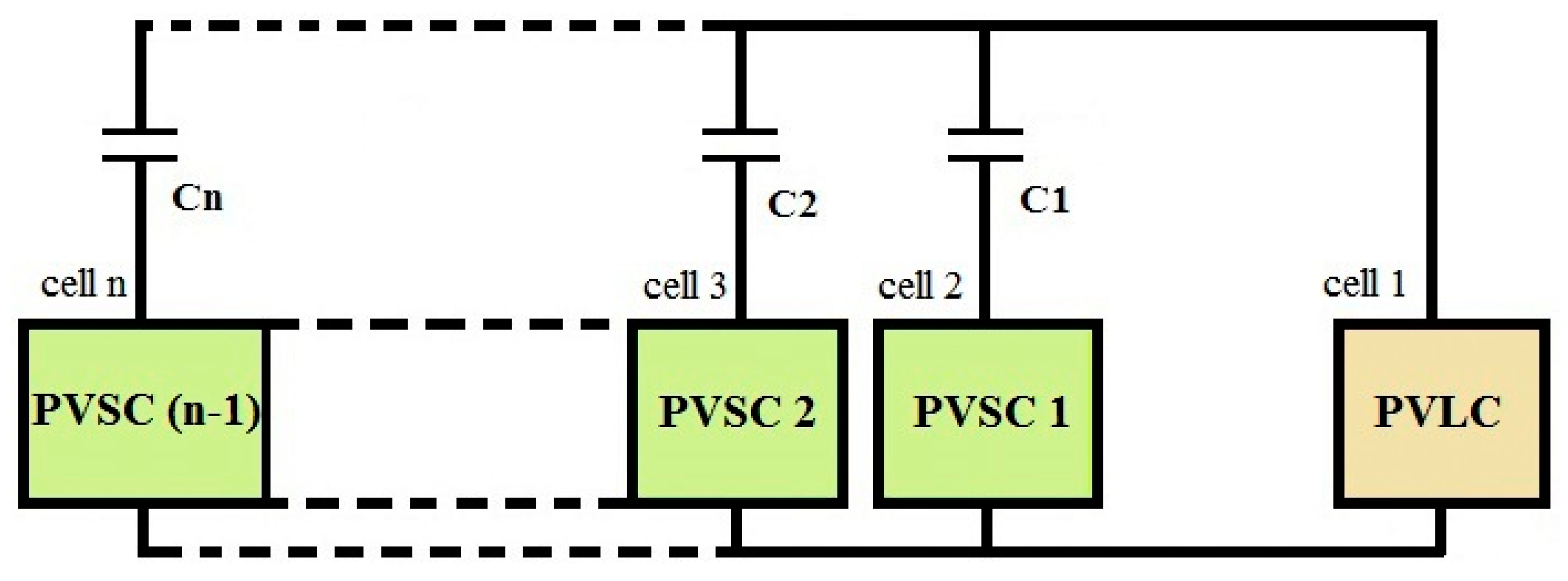
Figure 3.
Generalized diagram of an n-port SEPIC converter.
Figure 3.
Generalized diagram of an n-port SEPIC converter.
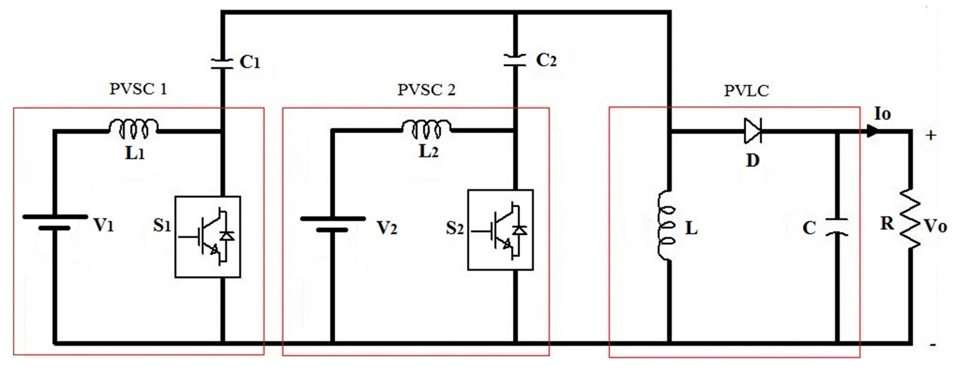
Figure 4.
A three-port unidirectional SEPIC converter (Topology-1).
Figure 4.
A three-port unidirectional SEPIC converter (Topology-1).
Figure 5.
Modes of operation.
Figure 5.
Modes of operation.
Figure 6.
Mode-1 of topology-1 (S1 and S2 ON, only S1 conducts).
Figure 6.
Mode-1 of topology-1 (S1 and S2 ON, only S1 conducts).
Figure 7.
Mode-2 of topology-1 (S1 OFF and S2 ON).
Figure 7.
Mode-2 of topology-1 (S1 OFF and S2 ON).
Figure 8.
Mode-3 of topology-1 (S1 and S2 OFF, D conducts).
Figure 8.
Mode-3 of topology-1 (S1 and S2 OFF, D conducts).
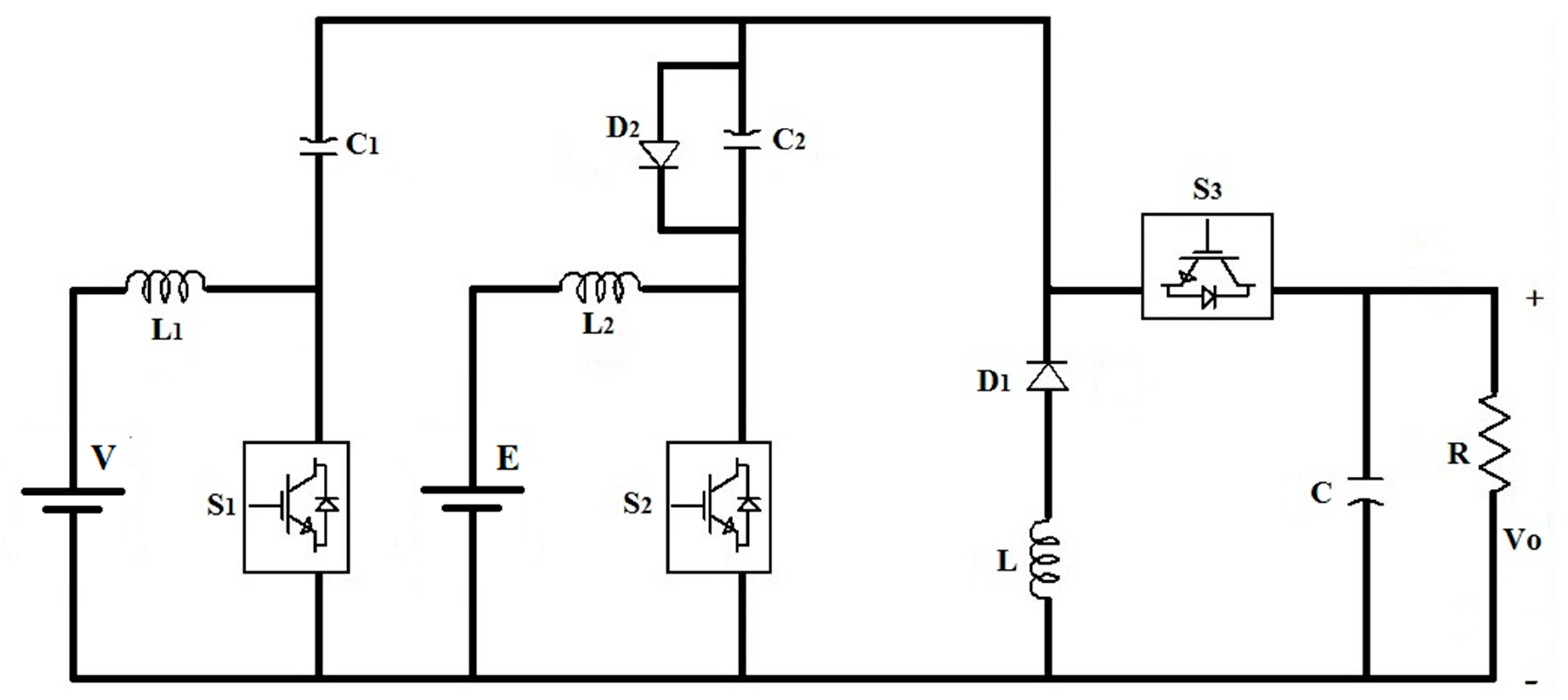
Figure 9.
Three-port bidirectional SEPIC converter (Topology-2).
Figure 9.
Three-port bidirectional SEPIC converter (Topology-2).
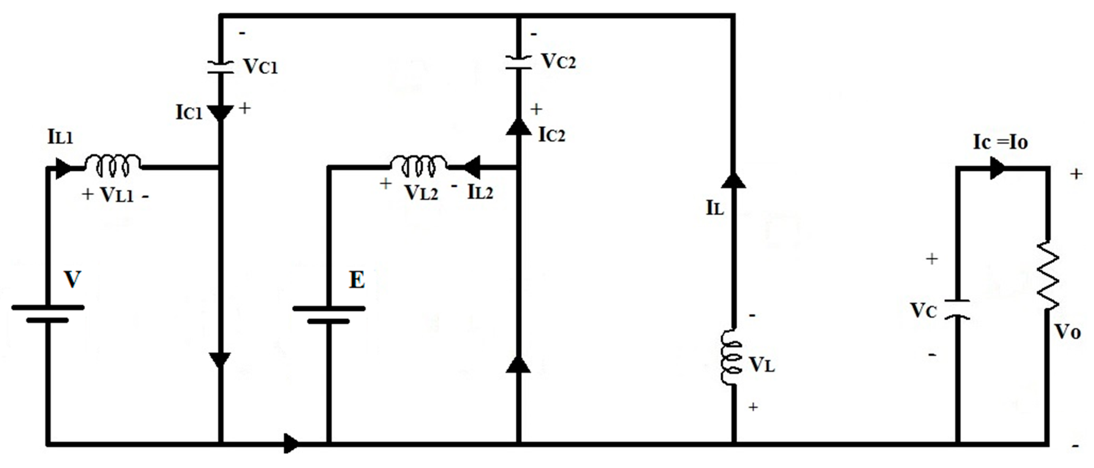
Figure 10.
Modes of operation (case 1, when V < E).
Figure 10.
Modes of operation (case 1, when V < E).
Figure 11.
Modes of operation (case 2, when V > E).
Figure 11.
Modes of operation (case 2, when V > E).
Figure 12.
Mode 1 of topology-2 (case-2).
Figure 12.
Mode 1 of topology-2 (case-2).
Figure 13.
Mode-2 of topology-2 (case-2).
Figure 13.
Mode-2 of topology-2 (case-2).
Figure 14.
Current and voltage waveforms of each component (switch, inductor, and capacitor) present in PVSC1, PVSC2, and PVLC of topology-1.
Figure 14.
Current and voltage waveforms of each component (switch, inductor, and capacitor) present in PVSC1, PVSC2, and PVLC of topology-1.
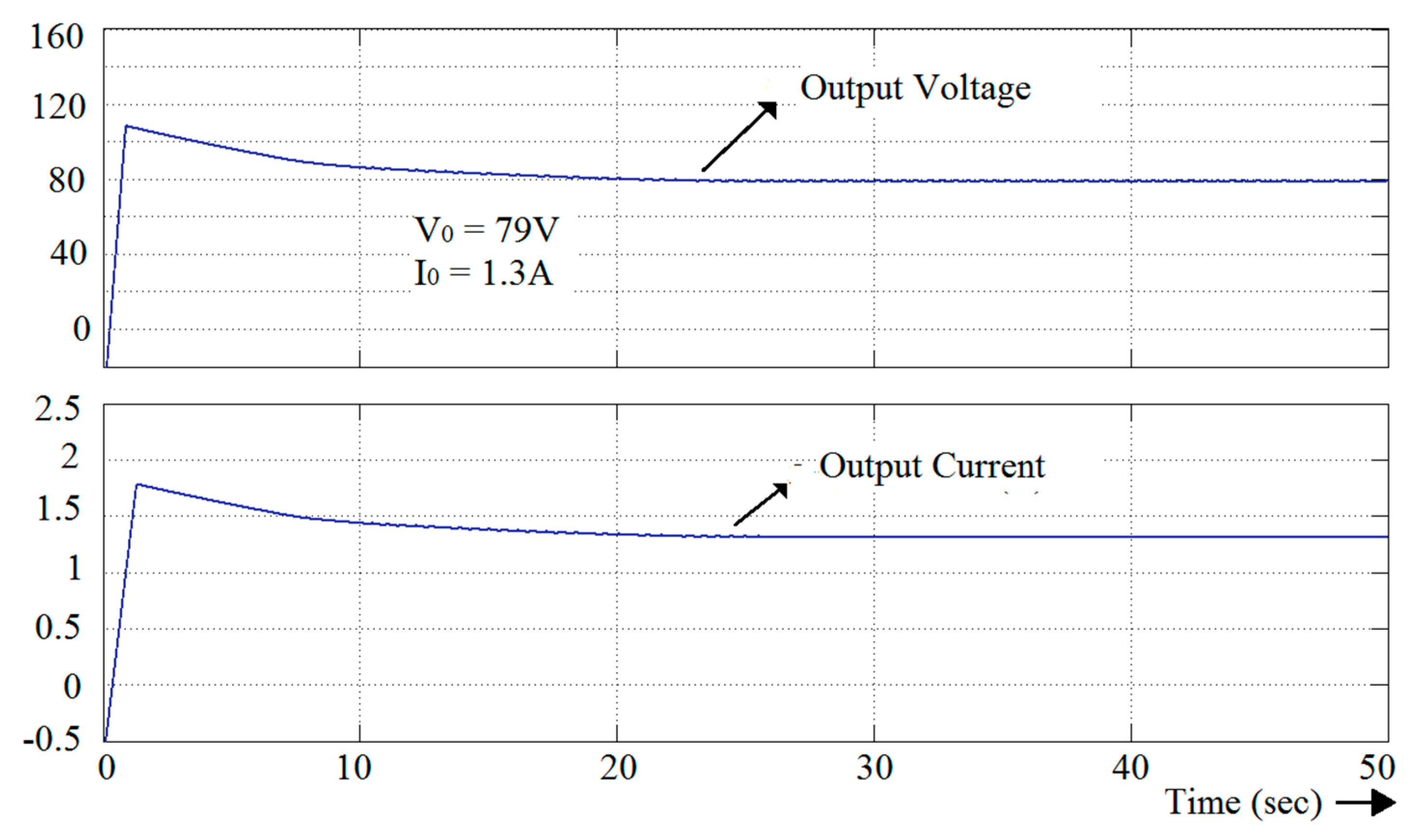
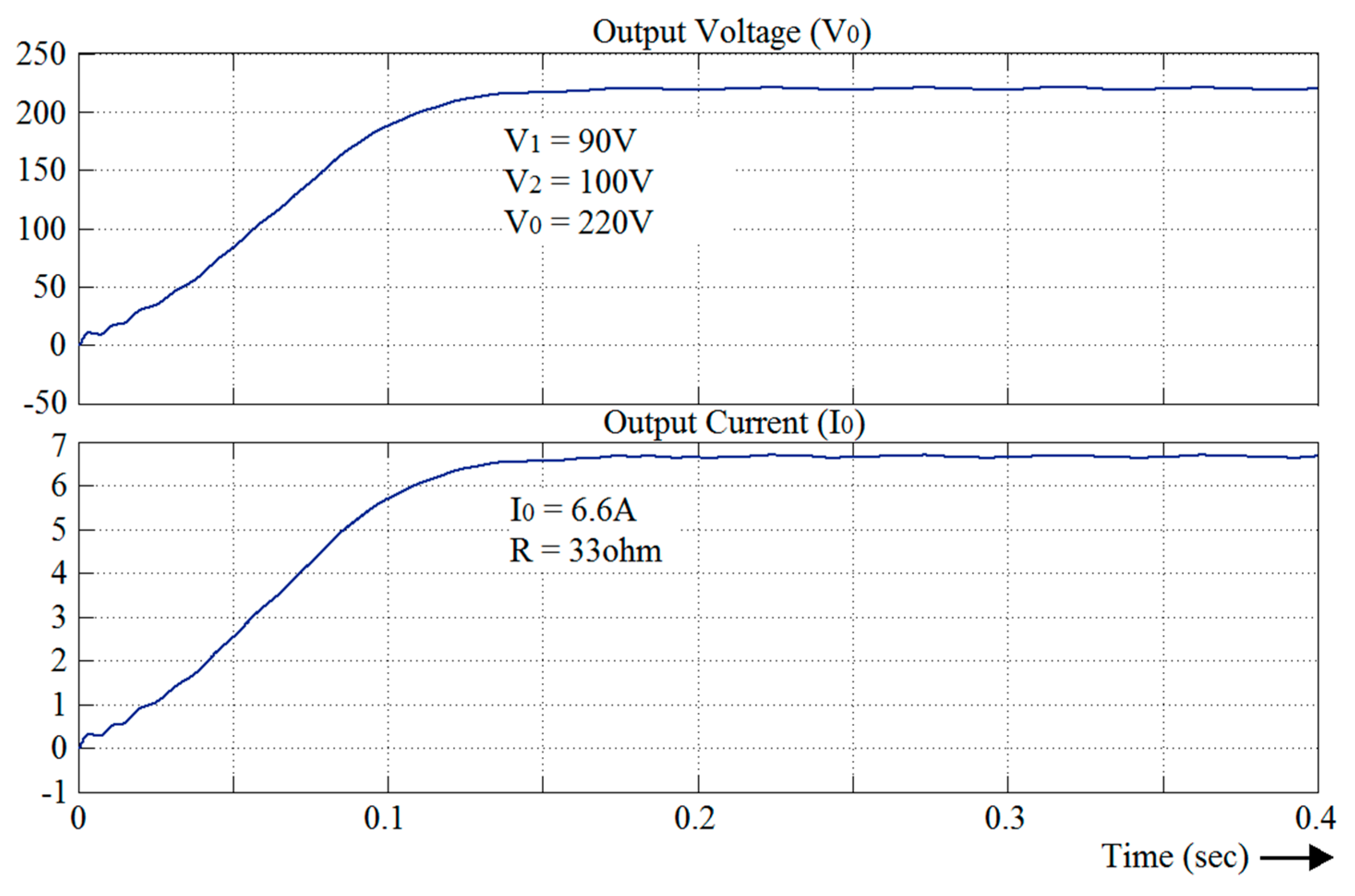
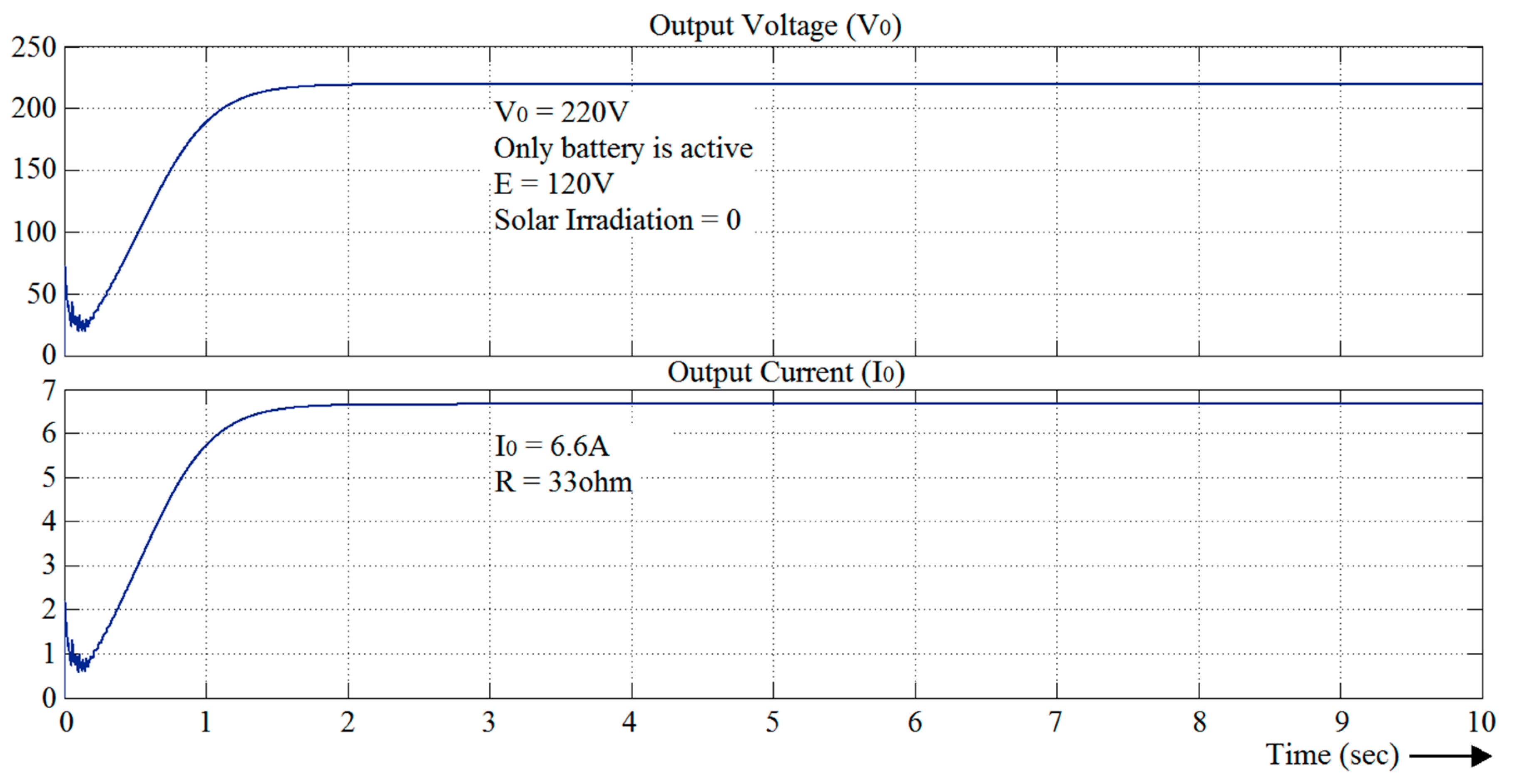
Figure 15.
Output voltage and current waveforms of topology-1.
Figure 15.
Output voltage and current waveforms of topology-1.
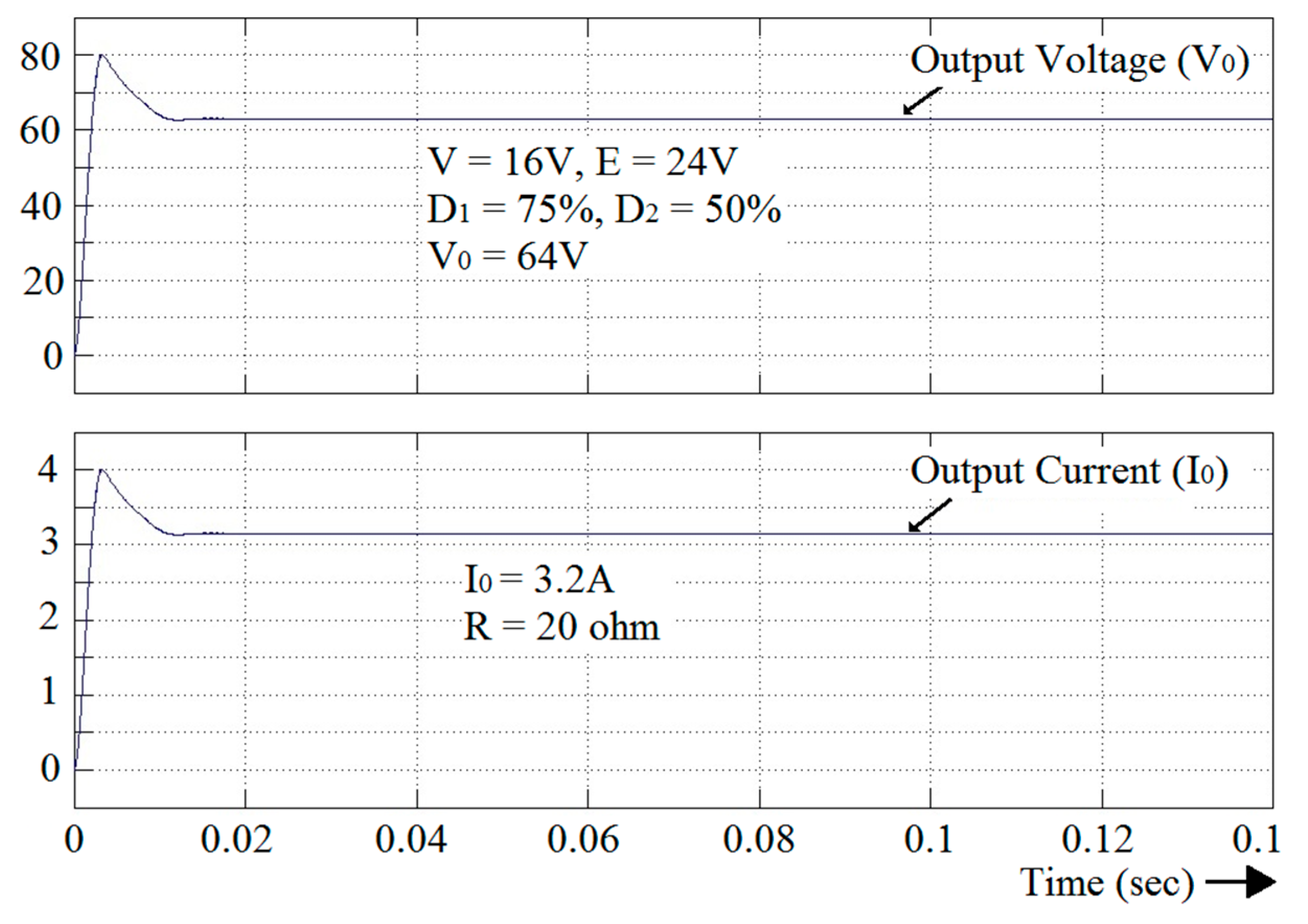
Figure 16.
Output voltage and current waveforms of topology-2 during discharging (case-1).
Figure 16.
Output voltage and current waveforms of topology-2 during discharging (case-1).
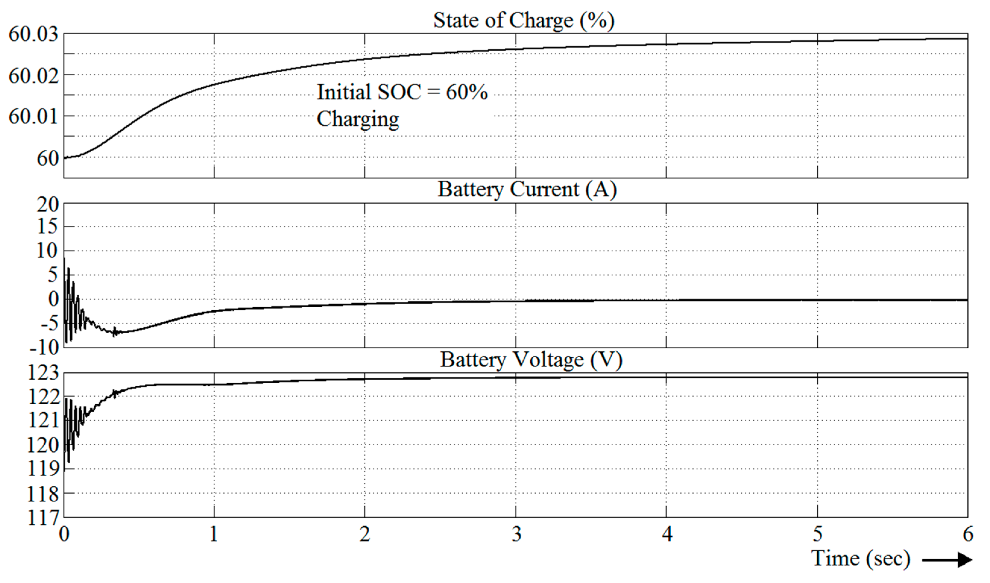
Figure 17.
State of charge, current, and voltage waveforms of battery for topology-2 during discharging (case-1).
Figure 17.
State of charge, current, and voltage waveforms of battery for topology-2 during discharging (case-1).
Figure 18.
Output voltage and current waveforms of topology-2 during charging (case-2).
Figure 18.
Output voltage and current waveforms of topology-2 during charging (case-2).
Figure 19.
State of charge (SOC), current, and voltage waveforms of the battery for topology-2 during charging (case-2).
Figure 19.
State of charge (SOC), current, and voltage waveforms of the battery for topology-2 during charging (case-2).
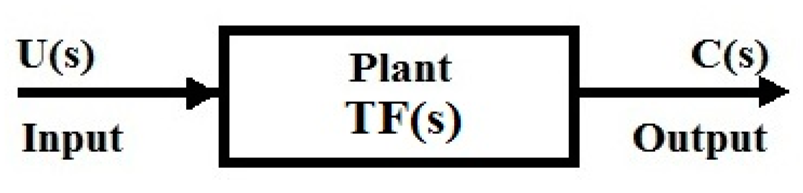
Figure 20.
Open-loop system block diagram.
Figure 20.
Open-loop system block diagram.
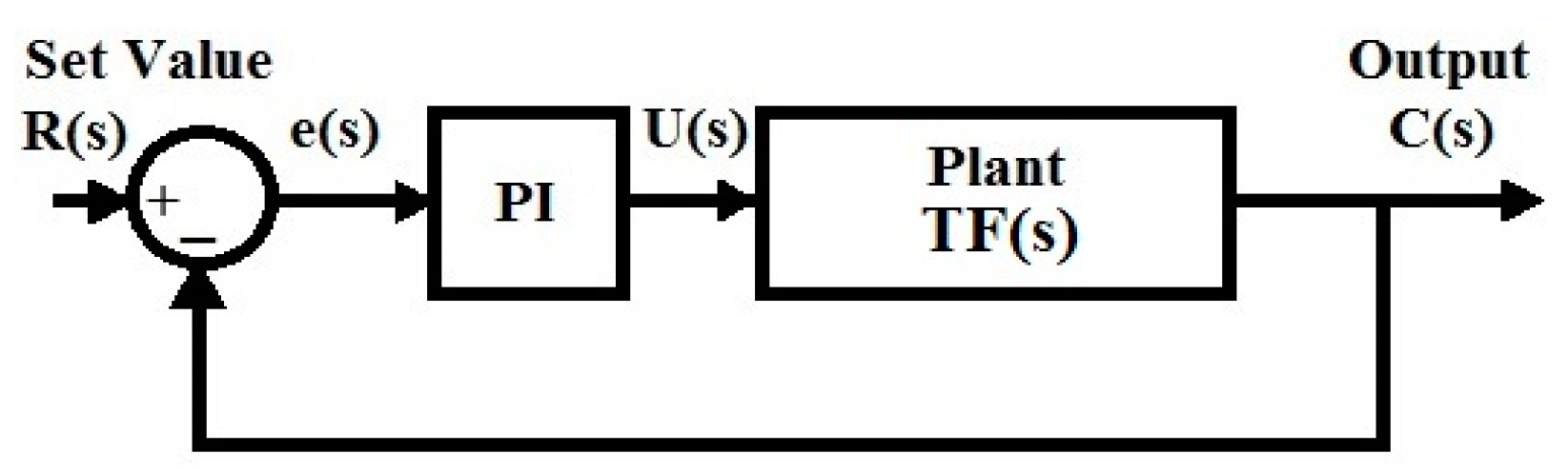
Figure 21.
Closed-loop system block diagram.
Figure 21.
Closed-loop system block diagram.
Figure 22.
Step response of the proposed converter for the open-loop and closed-loop systems.
Figure 22.
Step response of the proposed converter for the open-loop and closed-loop systems.
Figure 23.
Unidirectional closed-loop converter.
Figure 23.
Unidirectional closed-loop converter.
Figure 24.
Output voltage and current of a unidirectional closed-loop converter.
Figure 24.
Output voltage and current of a unidirectional closed-loop converter.
Figure 25.
Bidirectional closed-loop converter.
Figure 25.
Bidirectional closed-loop converter.
Figure 26.
PV input, output voltage, and current during intermittent solar irradiation.
Figure 26.
PV input, output voltage, and current during intermittent solar irradiation.
Figure 27.
Output voltage and current of a bidirectional closed-loop converter when both the PV and battery are supplying (condition-1 of control logic).
Figure 27.
Output voltage and current of a bidirectional closed-loop converter when both the PV and battery are supplying (condition-1 of control logic).
Figure 28.
SOC, current, and voltage of the battery during discharging (condition-1 of control logic).
Figure 28.
SOC, current, and voltage of the battery during discharging (condition-1 of control logic).
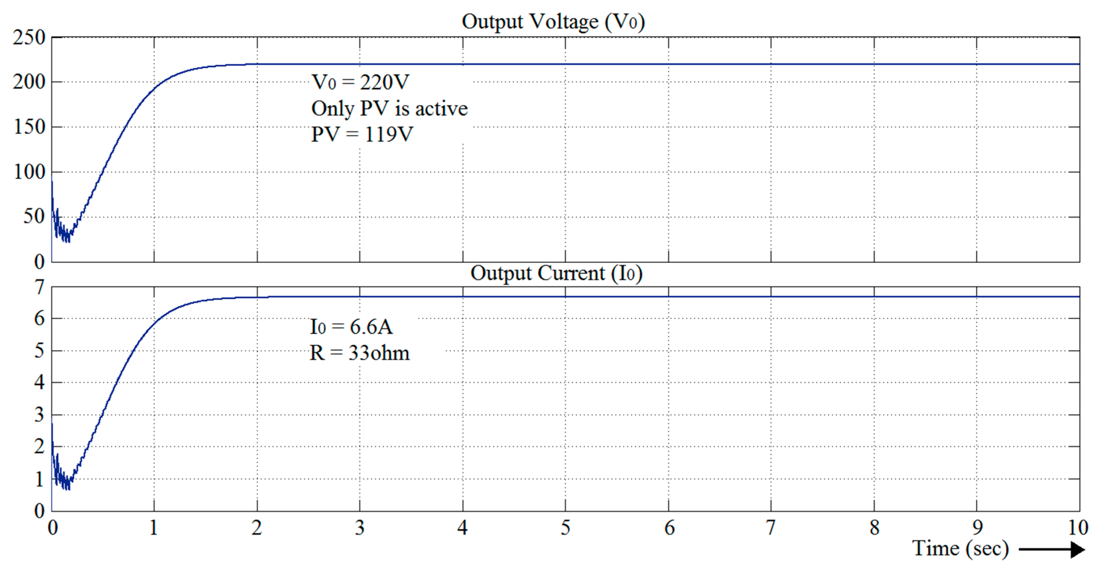
Figure 29.
Output voltage and current of a bidirectional closed-loop converter when only the PV is supplying (condition-2 of control logic).
Figure 29.
Output voltage and current of a bidirectional closed-loop converter when only the PV is supplying (condition-2 of control logic).
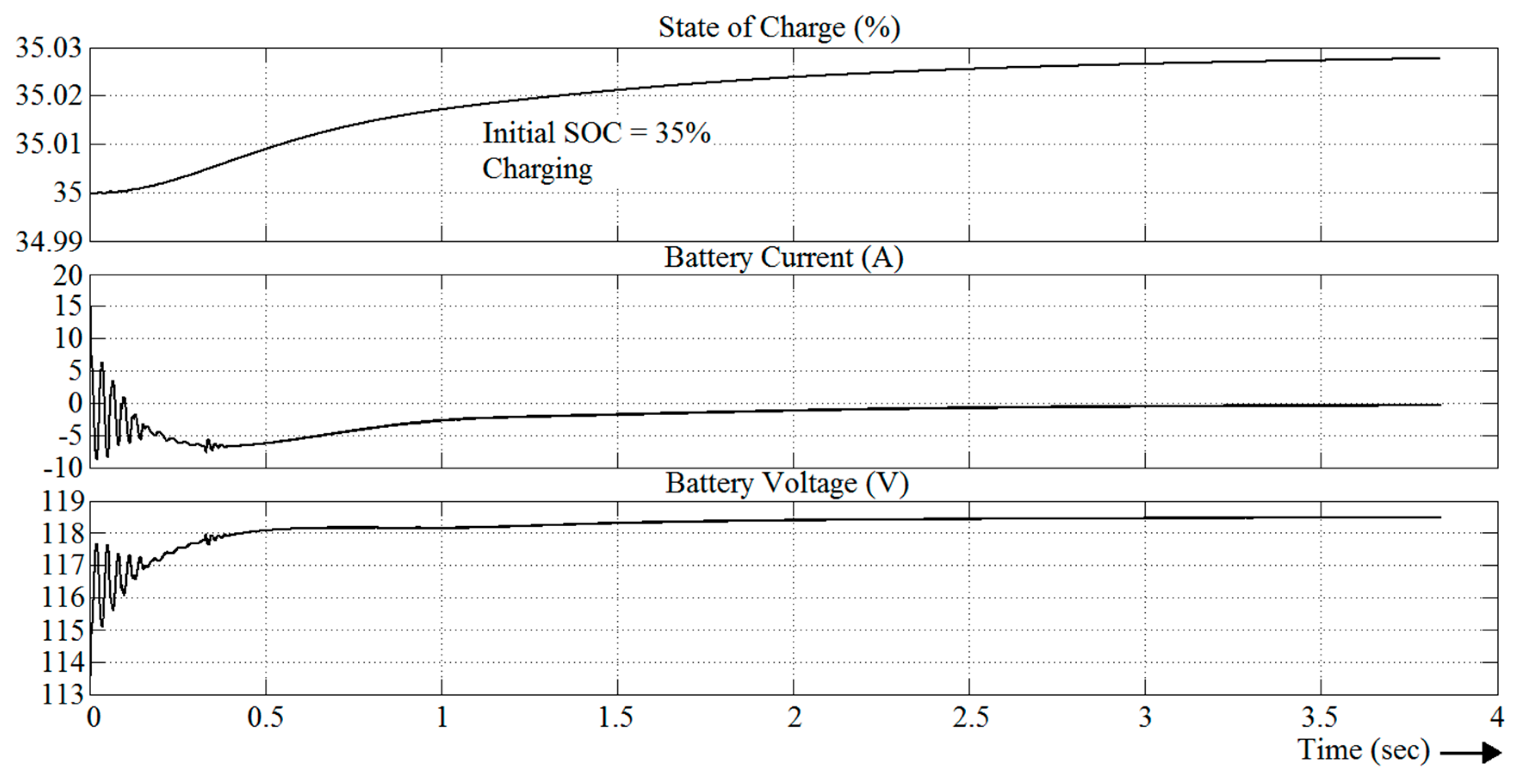
Figure 30.
SOC, current, and voltage of the battery during charging (condition-2 of control logic).
Figure 30.
SOC, current, and voltage of the battery during charging (condition-2 of control logic).
Figure 31.
Output voltage and current of a bidirectional closed-loop converter when only the solar PV is supplying, and the battery is fully charged (Condition-3 of control logic).
Figure 31.
Output voltage and current of a bidirectional closed-loop converter when only the solar PV is supplying, and the battery is fully charged (Condition-3 of control logic).
Figure 32.
SOC, current, and voltage of the battery when it is fully charged (Condition-3 of control logic).
Figure 32.
SOC, current, and voltage of the battery when it is fully charged (Condition-3 of control logic).
Figure 33.
Output voltage and current of a bidirectional closed-loop converter when only the solar PV is supplying, and the battery is undercharged (Condition-4 of control logic).
Figure 33.
Output voltage and current of a bidirectional closed-loop converter when only the solar PV is supplying, and the battery is undercharged (Condition-4 of control logic).
Figure 34.
SOC, current, and voltage of the battery when it is undercharged (Condition-4 of control logic).
Figure 34.
SOC, current, and voltage of the battery when it is undercharged (Condition-4 of control logic).
Figure 35.
Output voltage and current of a bidirectional closed-loop converter when only the battery is supplying (Condition-5 of control logic).
Figure 35.
Output voltage and current of a bidirectional closed-loop converter when only the battery is supplying (Condition-5 of control logic).
Figure 36.
SOC, current, and voltage of the battery (Condition-5 of control logic).
Figure 36.
SOC, current, and voltage of the battery (Condition-5 of control logic).
Figure 37.
Hardware setup of the proposed topology-1.
Figure 37.
Hardware setup of the proposed topology-1.
Figure 38.
(a) Input voltages (V1 = 35 V, V2 = 42 V), (b) switching pulses for S1 and S2 (D1 = 67% and D2 = 50%).
Figure 38.
(a) Input voltages (V1 = 35 V, V2 = 42 V), (b) switching pulses for S1 and S2 (D1 = 67% and D2 = 50%).
Figure 39.
(a) Voltages across switches S1 and S2 (Vt1 and Vt2), (b) currents through inductors L1 and L2 (iL1 and iL2).
Figure 39.
(a) Voltages across switches S1 and S2 (Vt1 and Vt2), (b) currents through inductors L1 and L2 (iL1 and iL2).
Figure 40.
(a) Voltages across the capacitors C1 and C2 (VC1 and VC2), (b) voltage across the output capacitor C (VC1).
Figure 40.
(a) Voltages across the capacitors C1 and C2 (VC1 and VC2), (b) voltage across the output capacitor C (VC1).
Figure 41.
Output voltage (V0 = 78.8 V).
Figure 41.
Output voltage (V0 = 78.8 V).
Table 1.
Simulation parameters.
Table 1.
Simulation parameters.
| Parameters | Estimated Values | Simulation Values | Unit |
|---|
| L1, L2 | 14.74 | 15 | mH |
| C1, C2 | 0.462 | 0.54 | mF |
| L | 14.74 | 15 | mH |
| C | 0.299 | 0.54 | mF |
| R | 60 | 60 | Ohm |
| V1 | 42 | 42 | V |
| V2 | 42 | 42 | V |
| D1 | 67 | 67 | % |
| D2 | 50 | 50 | % |
| f (switching freq.) | 10,000 | 10,000 | Hz |
Table 2.
Comparison of the simulated and estimated results of topology-1.
Table 2.
Comparison of the simulated and estimated results of topology-1.
| V1 (Volt) | V2 (Volt) | D1 (%) | D2 (%) | Sim. VO (Volt) | Est. VO (Volt) |
|---|
| 24 | 12 | 30 | 60 | 28.5 | 27 |
| 30 | 15 | 30 | 60 | 36 | 33.75 |
| 25 | 20 | 55 | 68.75 | 50 | 52.8 |
| 30 | 20 | 50 | 75 | 77 | 80 |
| 36 | 24 | 40 | 60 | 52 | 48 |
| 36 | 24 | 50 | 75 | 92 | 96 |
| 35 | 42 | 67 | 50 | 79 | 81.66 |
Table 3.
Comparison of the simulated and estimated results of topology-2 during discharging (case-1).
Table 3.
Comparison of the simulated and estimated results of topology-2 during discharging (case-1).
| V (Volt) | E (Volt) | D1 (%) | D2 (%) | Sim. VO (Volt) | Est. VO (Volt) |
|---|
| 8 | 12 | 82.5 | 55 | 49 | 50.28 |
| 10 | 12 | 62.4 | 52 | 21 | 19.4 |
| 20 | 24 | 72 | 60 | 61 | 60 |
| 16 | 24 | 75 | 50 | 64 | 64 |
| 30 | 36 | 75 | 50 | 104 | 102 |
| 20 | 36 | 72 | 40 | 75 | 74.28 |
Table 4.
Comparison of the simulated and estimated results of topology-2 during charging (case-2).
Table 4.
Comparison of the simulated and estimated results of topology-2 during charging (case-2).
| V (Volt) | E (Volt) | D1 (%) | D2 (%) | Sim. VO (Volt) |
|---|
| 20 | 12 | 60 | 39.5 | 38 |
| 15 | 12 | 70 | 39.3 | 38 |
| 30 | 24 | 60 | 53.3 | 51 |
| 20 | 12 | 40 | 23 | 21.3 |
| 40 | 24 | 60 | 80 | 76 |
| 44 | 36 | 50 | 63 | 52 |
| 40 | 36 | 60 | 66.5 | 64 |
Table 5.
Control logic of a closed-loop bidirectional controller.
Table 5.
Control logic of a closed-loop bidirectional controller.
| Condition | SOC | vpv | irr | batcut | pvcut | pvmpp | batpi |
|---|
| 1 | >80% | - | - | 1 | 1 | 1 | 1 |
| 2 | <95% | >120 | - | 1 | 1 | 0 | 0 |
| 3 | >99% | >120 | - | 0 | 1 | 0 | 0 |
| 4 | <40% | - | - | 1 | 1 | 0 | 0 |
| 5 | - | - | 0 | 0 | 1 | 1 | 1 |
Table 6.
Design parameters for the hardware setup.
Table 6.
Design parameters for the hardware setup.
| Description | Specification |
|---|
| PVSC1 inductor, L1 | 15 mH |
| PVSC2 inductor, L2 | 15 mH |
| PVLC inductor, L | 15 mH |
| PVSC1 capacitor, C1 | 0.54 mF |
| PVSC2 capacitor, C2 | 0.54 mF |
| PVLC capacitor, C | 0.54 mF |
| Switching frequency, f | 10,000 Hz |


