Abstract
With a view to regulate the output voltage with fixed frequency, without using any additional component or complex modulation technique, a topology of a variable duty controlled three-level LLC converter is proposed and an equivalent small signal model for Electric Vehicle (EV) charger applications is deduced in this paper. The steady state equations of each operating region are derived in time domain. Based on an Extended Describing Function (EDF) approach, a small signal equivalent circuit is modeled which includes both frequency and duty controlled terms. The equivalent circuit is further simplified to derive a transfer function of duty control to output voltage. The transfer function is verified through simulation software. Analyzing the transfer function, a voltage controller is designed and implemented with a PI compensator. The simulation results of the proposed control schemes are illustrated and discussed. The topology is compared to a conventional frequency control topology and the merits of the proposed topology are presented.
1. Introduction
Electricity based transportation methods are being researched all over the world for the past two decades [1] in order to find alternatives to fuel consumption [2,3]. Electric Vehicle (EV) charger systems have been attracting great attention of researchers, manufacturers and governmental agencies as concerns for energy conservation and environmental issues are growing everyday [4,5,6]. In the architecture of such a charger, a DC-DC converter is an essential element. From the DC link voltage supplied by the Power Factor Corrector (PFC), the DC-DC converter charges the battery through the transformer [7,8]. LLC converters have been a widespread choice for the DC-DC converter stage in EV chargers [9,10,11,12]. This type of converter is capable of achieving Zero Voltage Switching (ZVS) at the switches and Zero Current Switching (ZCS) at the rectifier diodes at almost all load conditions. It also offers a wide gain range and undergoes low conduction losses or electromagnetic interference [13,14,15].
An extensive amount of research has been conducted on frequency modulated LLC converter for simpler control and calculation [16,17,18,19]. However, frequency variation is conducted over a wide range resulting loss of ZVS [20] and introduces ripple [21] at certain load conditions. In [22], an additional three-level buck converter has been used to regulate the output voltage. A T-type three-level unit along with a LLC converter is applied with switch multiplexing technique [23]. The RMS value of current flowing through the secondary diodes have been reduced in [24], however, several control modes are required to regulate the converter at rated voltage. Recently, pulse-width or duty cycle modulation are gaining interest for wide gain range [25,26], enhanced light load efficiency [27,28] and suppressed inrush current [29]. The output can be well-regulated by adding a duty cycle in the input of the resonant tank and no loss of ZVS occurs in case of duty control at any load condition. Since the switching frequency is fixed in the duty controlled converter, the magnetic components optimization is also convenient.
The reported applications of three-level LLC converters are limited in number [30,31,32,33,34,35,36,37,38,39,40] compared to conventional two-level converters. The voltage stress is half of the input voltage in the case of three-level converters and is advantageous for high switching frequency and higher efficiency [30]. If the switching frequency is chosen equal to resonant frequency and the ratio of resonant inductor to magnetizing inductor is smaller, voltage gain tolerance will be minimum [31]. The modulation technique in [32] with six switches is complex. Variation of output with change in frequency has been reported in [33]. The voltage is not equal to half for all loads and voltage gain in [34]. The lagging leg in [35] complicates the design and the current stress across that switch is high. Even though the converter in [36] uses fixed frequency scheme, the voltage stress in two lagging leg switches is equal to half of the input voltage. In [37], the converter is frequency controlled and calculation of additional dead time zones are required. The three-level LLC in [38] split the resonant capacitor and application of variable duty cycle is not suitable in this topology. There are eight inverter switches [39] and switching sequences can lead to complex control schemes. Nevertheless, the waveforms are highly nonlinear and the real time calculation is far more complex than frequency controlled LLC converters. A combined sliding mode control and PI control mode have been adopted in [40] for full bridge LLC converters based on an averaged large signal model. But the transfer function for PI control had to be derived through system identification method due to nonlinear behavior of the circuit. To linearize the circuit and implement a control strategy, a small signal modeling approach can be undertaken.
Although the state plane average method [41] is widely applied for PWM converters, it provides a solution up to half of the switching frequency only. Again, the sample data approach method in [42] offers a numerical way to design the compensator, which is difficult to apply. Extended Describing Function (EDF) is the preferred choice for small signal modeling approach for series/parallel resonant converters [43,44,45]. It is applied from the input to the output through the resonant tank. The modeling is based on first harmonic approximation of the state variables and then a set of functions is generated relating the input, state variables and control variables. The EDF method applied for LLC converter in [43,44] leads to an equivalent circuit model of fifth order. The complex terms in the functions can be withdrawn by separating the circuit into sine and cosine part and introducing cross coupled terms. In [45], the equivalent circuit is reduced to a simplified third-order circuit but for variable switching frequency control only.
In this paper, a three-level duty controlled circuit topology is proposed. The steady state waveforms are expressed by equations in time domain. The steady state behavior is observed through simulation results. With the aim of linearizing the circuit and developing a duty control to output voltage transfer function, an equivalent small signal model approach has been modeled applying the reduced third order EDF concept. Upon deriving the transfer function, it is verified by simulation. An output voltage PI controller is designed by compensating the derived transfer function. The simulation results are obtained for output by varying the reference voltage and load resistance. Lastly, a comparison between steady state wave forms of frequency control and duty control method is presented and a conclusion is drawn.
2. Duty Cycle Controlled Three-Level LLC Converter
The proposed converter consists of a dc source, two capacitors at the input, followed by the clamping diodes and a resonant tank. The rectifier along with the capacitive filter and load are separated by an isolating transformer. The circuit schematic and equivalent circuit are given in Figure 1a,b, respectively.
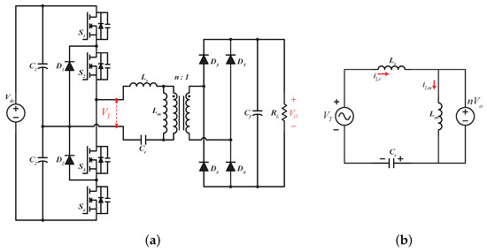
Figure 1.
Proposed three-level LLC converter: (a) circuit schematic; and (b) equivalent AC circuit.
The input dc source voltage is split in half by and . The voltage is clamped by the diodes and . The half bridge configurations consist of four switches from to in series. A square voltage is generated at the input of the resonant tank, , whose amplitude is equal to the half of the input dc source voltage i.e., . The resonant tank consists of a resonant inductor , resonant capacitor , and a magnetizing inductor in series. The tank is followed by an isolating transformer of turns ratio n. The output side contains diode rectifiers –, a capacitive filter and a resistive load .
The resonant frequency and the magnetizing frequency of the converter are given by:
In a duty controlled converter, the switching frequency is fixed and, in the proposed converter, the switching frequency is chosen equal to the resonant frequency. The normalized parameters of the converter are given by,
where is the normalized tank impedance at resonant frequency, d is the normalized tank impedance at magnetizing frequency, is the ac equivalent resistance, m is the inductance ratio and Q is the quality factor.
According to Figure 1b, generalized state space equations are given below:
2.1. Operation of the Proposed Duty Control
The voltage and the current waveforms in the proposed three-level duty controlled topology mainly operate at six different modes. The positive half cycle is comprised of six operating regions – and the remaining three are in the negative half cycle having similar equations as the positive cycle, only opposite in polarity. The passive elements, switches and the diodes are assumed to be ideal and the short dead time is ignored. In this paper, the switches and are duty cycle controlled (≤0.5) and the corresponding switches and are constantly driving signals at alternating cycles. One switching period is given by . Compared to the conventional frequency controlled LLC converter, the duty controlled converter has an additional operating region, which leads to a complex analysis of the circuit parameters. The switching sequences and the key operational waveforms are depicted in Figure 2.
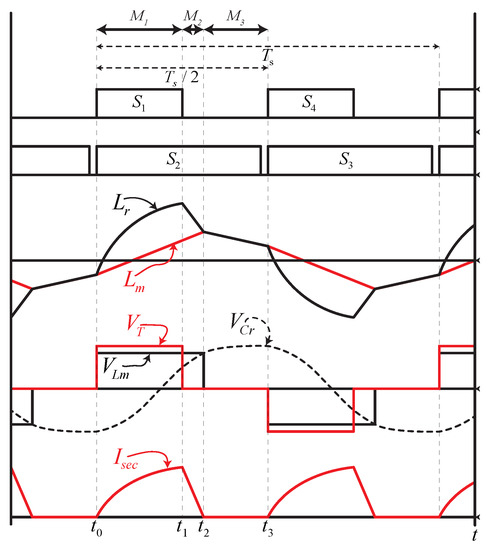
Figure 2.
Operational Waveforms in duty controlled three-level LLC converter.
2.2. Steady State Operation of Operation Modes
Analyzing the state space equations and incorporating the initial conditions, the steady state equations of each operating region can be obtained. The steady state equations are discussed below and the respective equivalent circuit is presented in Figure 3a–c.
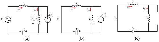
Figure 3.
Equivalent steady-state circuit during: (a) Mode 1; (b) Mode 2; and (c) Mode 3.
- Mode 1 (): [From to ]
As shown in Figure 2, at , switches and turn on. A square wave voltage is produced at the input of the tank. Both and start linearly increasing from their negative value and reach a positive value by time . The output voltage is clamped by and transferred to the secondary. The output rectifier maintains ON state. The conduction period of this mode is equivalent to . The derived steady state equations of this mode in time domain are given below:
where , and are the resonant current, magnetizing current and resonant capacitor voltage at time and also are the initial conditions of the positive half cycle. The equivalent circuit is shown in Figure 3a.
- Mode 2 (): [From to ]
The converter operation reaches its second stage at time when only switch is conducting and is turned off. Contrary to frequency controlled LLC converter where the tank input voltage remains positive in the positive half cycle, and negative in the next cycle, the square wave voltage drops to zero, consequently starts to decrease. is still increasing linearly. The energy difference between and is transferred to the secondary side. In this mode also, the output rectifiers maintain ON state. The steady state equations of this mode are the following:
- Mode 3 (): [From to ]
continues to decrease and at time it is equal to , which leads the converter to operate in its third operating interval. From to , the resonant current circulate around the tank and is equal to . Both the input voltage and the output voltage are zero. The output rectifiers are in OFF state and no energy is transferred to the output. The equations expressing the behavior of the waveform in this interval are:
The initial values of the operating waveforms are:
2.3. Power Transfer Stage
The difference in energy between and during the time from to is transferred to the secondary side as output. The output rectifier current can be expressed as:
As evident from Equation (8), the steady state solution is complex, non-linear and cumbersome to calculate. However, deriving the solution is not within the scope of this paper. From the next section onward, equivalent small signal modeling of the duty controlled LLC converter is discussed.
3. Equivalent Small Signal Circuit Modeling
3.1. Modeling with Extended Describing Function
In steady state operation the waveforms of the converter can be approximated as sinusoidal [41]. The resonant current, magnetizing current and the resonant voltage can be expressed in the form of their fundamental harmonic in the following manner splitting into sine and cosine parts:
where, is the angular switching frequency.
The derivatives of , , are:
where, , , and are the sine and cosine component of the fundamental approximation of resonant current and magnetizing current respectively.
The input and the output waveforms of the inverter are approximated by the DC components whereas the resonant tank waveforms can be approximated by fundamental approximation.
where d is the input duty cycle, is the input dc voltage signal and equal to in the three-level LLC Converter, is the input current signal and is the output voltage signal.
The functions ∼ are termed as EDF terms [43,44]. The EDF terms are obtained by applying Fourier transform to the nonlinear equations from Equation (3) and are shown in the following:
In small signal modeling, the modulation frequency is lower than the switching frequency and thus can be considered to operate in steady state condition. Substituting the Equations (10)–(12) in (3) and equating the coefficients of dc, sine and cosine terms the following harmonic balance is established
Thus, the output equation can be written as:
When the proposed LLC converter is operating at steady state the derivative terms are considered equal to zero. In addition, when all the switches are operating at a duty cycle of 50%, the steady state solution is similar to typical two level converters and is given by:
where is the normalized frequency given by . The circuit is linearized and perturbed around the point by replacing as the following,
where , D and are the quiescent values of the input voltage, duty and switching frequency waveforms and are the small ac variations respectively. The EDF method is applied from the input to the output including the resonant tank. The inverter receives an input voltage from a dc source and generates a high frequency square wave . The rectifier transforms this ac current to dc current. If switching frequency is near or equal to resonant frequency, the higher order harmonics are discarded by the resonant tank. Therefore the input and output of the converter is dominated by dc component whereas the tank is dominated by fundamental component. The average input current is directly proportional to the duty cycle d and indirectly proportional to the switching frequency since the resonant current varies the switching frequency as can be seen from Equation (13). The square wave voltage is perturbed to yield the duty controlled voltage source [44],
The inductances of the tank is also characterized by their respective complex switching frequency impedance and complex controlled voltage source due to perturbation of switching frequency. The same can be modeled for the resonant capacitor. The resonant capacitor can be replaced with an equivalent inductor when the modulation frequency is very small than the switching frequency and the current source parallel to the capacitor is replaced by an equivalent voltage source [45]. The resonant inductor, magnetizing inductor and resonant capacitor can be replaced by an equivalent series inductor . Although the tank waveforms are dominated by modulation frequency which again dependent on the switching the frequency, the duty controlled input current produces a duty controlled output at the output of the resonant current. The average component of the rectified current can be expressed as the average value of the resonant current [43,44]. In [43,44], the complex terms were withdrawn by separating the sine and cosine terms and introducing cross coupled terms. The model is further reduced to a simplified third order in [45]. The equivalent inductance can be represented by and can be expressed as,
The tank impedance at switching frequency is given by Z where Z is given by,
The steady state voltage across the resonant capacitor in the sine and cosine part are given by and , and can be expressed by the resonant current divided by the capacitance, such as
The switching frequency dependent voltage source of the resonant inductor and resonant capacitor and can be combined into one source as and in the real and imaginary part respectively where,
The resonant current and are split into the magnetizing current , and the remaining flows into the output of the tank as and such as,
where,
and,
where, = . The cross coupling coefficients between the output of the inverter and input of the rectifier side for the real and imaginary part can be expressed as the following,
where,
The equivalent circuit of small signal model of three-level LLC including both frequency and duty controlled terms are given in Figure 4.
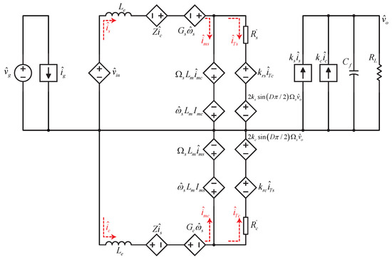
Figure 4.
Equivalent small signal model for both duty and frequency controlled LLC converter.
3.2. Equivalent Circuit for Duty Control to Output
In order to derive duty control to output voltage transfer function the model is Figure 4 must be further simplified by keeping the terms containing and and discarding frequency controlled terms since the converter operates with a fixed frequency in a duty controlled converter. Again, since the fixed frequency is equal to the resonant frequency the term becomes one, and from Equation (23) subsequently the parameter dependent on this term becomes zero. This results into being zero since it is dependent on as shown in Equation (24). Again, due to the same dependency on , the terms ,, , become zero from Equation (25). From Equation (15) it is apparent that at resonant frequency, the value of the magnetizing inductor, doesn’t affect the gain of the converter. In addition, the output current is dependent on the average value of the resonant current. In order to simplify the analysis, the controlled voltage sources associated with are discarded. At resonant frequency the impedance Z can be expressed as,
where, is the resonant frequency.
At resonant frequency, the impedance Z will also become zero. Consequently, the cosine loop is decoupled and only the upper loop is taken into consideration. Therefore the model depicted in Figure 4 is further reduced as shown in Figure 5.
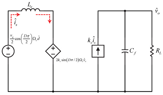
Figure 5.
Simplified equivalent circuit for deriving duty control to output voltage transfer function.
Applying KVL to both the loops at the right and left, the following equations are obtained:
By solving the Equation (27), the transfer function of variable duty cycle control to output voltage is derived as the following:
Evidently from Equation (28), the transfer function is of second order unlike the frequency controlled converter which is of third order and the output is dependent on the values of D, , , and . The obtained transfer function is verified through simulation and an output voltage controller is designed shown in the following in section.
4. Simulation Verification & Controller Design
The proposed circuit schematic was simulated using the PSIM simulation software. The parameters of the converter are given in Table 1.

Table 1.
Simulation parameters of the proposed three-level LLC Converter.
4.1. Simulation Results of Steady State Characteristics
The simulation results are obtained to observe the dependency of the steady state operations with variable duty and load. The simulation results at different duty cycle and load conditions are shown in Figure 6. As can be seen from Figure 6a–c the currents and increases linearly till and decreases from that time onward. The shape of is sinusoidal and reaches a positive/negative peak at the end of each positive/negative half cycle. When the duty cycle is increased in Figure 6b the interval and decreases since the interval is directly proportional to the duty cycle term and each half cycle is the sum of the three intervals. Again in Figure 6c, at low load condition, the resonant current drops to the quickly compared to high load condition and circulates around the resonant tank. All the key waveforms of the converter are dependent on both duty cycle and load which increases the non-linearity of the equations. In addition, as can be seen from Figure 6, ZVS is achieved in all conditions of duty and load.
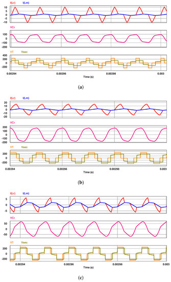
Figure 6.
Simulation results for steady-state operations of three-level LLC converter operating on input voltage at 500 V: (a) , ; (b) , ; (c) , .
The simulation is also carried out to check the output sensitivity for resonant and magnetizing parameters. The parameters from Table 1 are increased and decreased in order to observe the change in output as a result of degradation of parameters. The duty is kept to 0.3 with respect to and and the value of load resistance is 30 ohm. When the parameters are as given in Table 1, the value of peak resonant current is 11.9 A, the peak magnetizing current is 1.5 A, the peak resonant capacitor voltage is 113.8 V whereas the output voltage is 114.6 V. The increase in values resonant parameters will result in a lower resonant frequency and decrease in values will cause the opposite. When the resonant inductor is replaced by a value of 26.565 H and that of resonant capacitor is changed to 105 nF and the magnetizing inductor is kept at 170 H, the peak is decreased to 11.1 A and the peak of is decreased to 103.42 V resulting in a output voltage of 110 V. Again, when is decreased to 24.12 H and is decreased to 95 nF, the output scenario is reversed. The peak is increased to 12.2 A whereas the peak of rises to 125.86 nF. The output voltage is increased to 119.43 V. The peak of decreases to 1.45 A and increases to 1.63 A in respective cases. When only is changed keeping the resonant parameters same as Table 1, the peak value of is increased to 1.6 A for the inductor value 161.5 H and decreased to 1.4 A for for the inductor value 178 H. However, the output voltage is not affected by the slight change in the value of magnetizing inductor. The waveforms remain undistorted in every case and is shown in Figure 7a–d respectively.
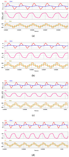
Figure 7.
Simulation results for (a) = 26.565 H, = 105 nF, = 170 H; (b) = 24.12 H, = 95 nF, = 170 H; (c) = 25.3 H, = 100 nF, = 161.5 H; (d) = 25.3 H, = 100 nF, = 178 H.
4.2. Simulation Verification of Small Signal Control to Output Transfer Function & Controller Design
The transfer function obtained in Equation (28) is verified by simulation through MATLAB software with the same parameters as given in Table 1, which generates a numerical transfer function. The bode plot of the analytical and numerical transfer functions are shown in Figure 8.
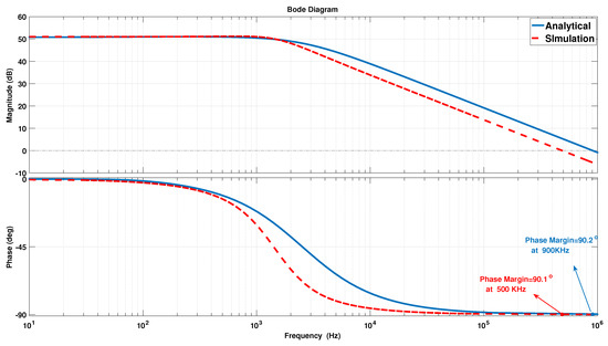
Figure 8.
Verification of the analytical transfer function with MATLAB software simulation.
Figure 8 shows a good match between the obtained analytical and simulation transfer function. Both the transfer functions are of second order and contains two poles and one zero. The phase margin of the analytical transfer function is 90.2° at 90 kHz and that of the numerical transfer function is 90.1° at 50 kHz. Both the bode plots show an infinite gain margin which states that the loops are stable. However, the bandwidth is very high to implement a voltage controller. Setting the desired phase margin 70 and overshoot <10%, a PI compensator is designed by adding an extra zero to the root locus plot and further tuning. The transfer function of the compensators for the analytical and simulated transfer functions are given below:
The uncompensated and compensated systems are plotted in Figure 9.
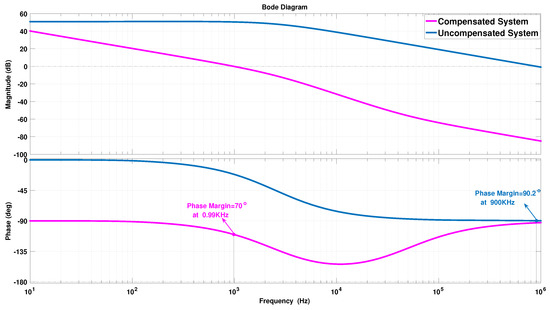
Figure 9.
Bode plot of PI tuned compensated system compared to the uncompensated system.
The bode plot of the compensated system shows a reduced bandwidth at the desired phase margin for both the analytical and simulation transfer function. The compensated transfer function is implemented as a simple PI controller transfer function to regulate the output voltage with a duty controlled signal. In a 3 level LLC converter, the expression for the gain is given by and since the operating frequency is equal to the resonant frequency, the gain cannot be higher than 1. Thus, the applied reference voltage must be equal to half or less than half of the input DC source voltage.
After the implementation of the PI compensator the simulation results are generated.
Firstly the controller results are verified for a fixed reference voltage. The simulation result of control signal, reference voltage, output voltage and output current is shown in Figure 10. For a 500 V input dc source, a 200 V reference was used as a reference voltage at 20 A load. The control signal is at first clamped at 0.5 which drops to 0.4 in accordance with the reference voltage.
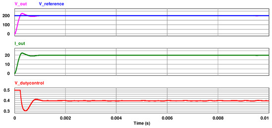
Figure 10.
Simulation results for duty controlled scheme for fixed reference voltage.
The controller results are also checked for parameter sensitivity. Since slight variation in doesn’t affect the output voltage, only resonant parameters are varied and shown in Figure 11. The and values are changed to 26.565 H and 105 nF respectively for the controller results shown in Figure 11a. Again, the values are altered to 24.12 H and 95 nF for the output presented in Figure 11b. In both the cases, the output can follow the reference.
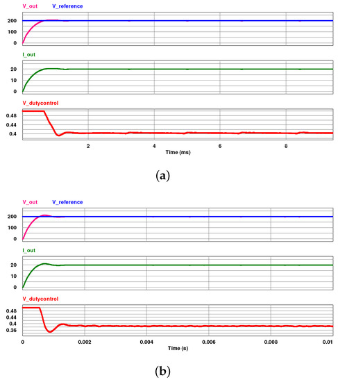
Figure 11.
Controller outputs for (a) = 26.565 H, = 105 nF, = 170 H; (b) = 24.12 H, = 95 nF, = 170 H.
A step value of 20 V was added to 200 V reference after 0.005 s to the converter when the input voltage source was of 500 V. The duty control signal increases and reaches to 0.4 simultaneously with the output voltage to follow the applied reference voltage of 200 V. As the step reference value is added after 0.005 s the duty controlled signal output follows the voltage reference. The duty cycle increased at 0.005 s from 0.4 to 0.44 and so does the output current.The controller can be further verified for varied load resistance for different input DC voltage for the controlled converter. The simulation results for added reference voltages and load resistances are presented in Figure 12.
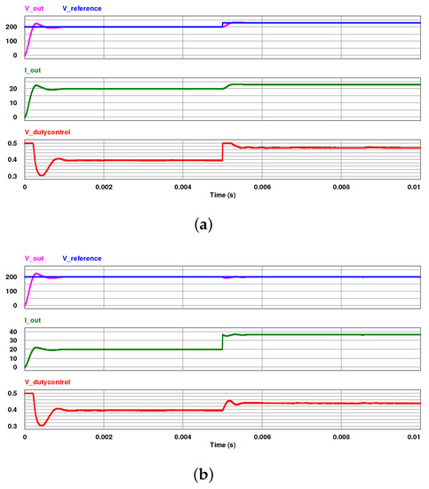
Figure 12.
Controller outputs for (a) Varied reference voltage; (b) Varied load resistance.
Figure 12b shows the simulation output of added load resistance after 0.005 s from the beginning of simulation which results in a slight drop in the output voltage at that instant. For both Figure 12a, and Figure 12b, the output follows the reference input.
The reduced small signal model is of second order, unlike the three order model for switching frequency control to output voltage and can be implemented with a simple PI compensator. To further validate the simplicity of the voltage regulation through duty control, the steady state waveforms are compared with the frequency controlled waveforms. The parameters of the converter are the same as listed in Table 1 and the value of the load resistance is kept at 50 . In order to obtain a desired output voltage of 120 V, input and output signals of both duty control and frequency control method in steady state are presented in Figure 13.
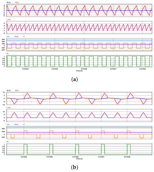
Figure 13.
Steady state waveforms of (a) Frequency controlled; (b) Duty controlled three-level LLC Converter.
Figure 13a shows the converter waveforms when the switching frequency is varied. To achieve a voltage as low as 120 V, the converter has to operate at a very high switching frequency. In this case, the switching frequency is required to regulate the voltage at 120 V is 340 K which is 3.4 times the resonant frequency of the tank. The high switching frequency can cause switching loss and decrease in efficiency. Moreover, the parameters of the converter should also be should be suitably optimized for frequency control for operating at wide range of frequencies. Further control methods have to be applied to obtain the desired output voltage at a reduced switching frequency. As the lighter load condition is approached, the required switching frequency becomes higher which ultimately results in large switching loss without ZCS of the rectifier diodes ∼. However, the duty control method is rather simple to implement and the desired output voltage can be achieved. The waveforms of duty controlled converter are presented in Figure 13b. In this case, the duty cycle value is tuned at 0.27 with respect to the switches and . If the load is further decreased, the applied duty cycle must be of greater value to get a lower output voltage than . Although both the duty control and frequency controlled outputs are dependent on load condition, the desired voltage for duty controlled converter can be achieved at the fixed switching frequency, only by adjusting the duty cycle. Thus the control is much simpler and causes minimum switching loss. The soft switching conditions are maintained at almost all load conditions. The optimization of parameters of the converter is not also as crucial as for the frequency controlled three-level LLC. converter. Therefore, the proposed topology can be regarded as a superior method in terms of simple and convenient control.
5. Conclusions
The proposed circuit topology of three-level duty controlled LLC converter is presented in this paper for a potential EV charger application. The modulation technique is rather simple and no additional component or circuitry has been required for controlling the output. The operating regions are discussed and the steady state equations of the respective regions are derived. The steady state waveforms are observed through simulation for different duty cycle and load resistance values. Using the EDF concept, a linearized small signal equivalent circuit is modeled for duty control to output voltage and a reduced second-order transfer function is derived. The transfer function is verified through simulation and compensated to design a voltage controller. The controller outputs are obtained for varying step reference voltage and load resistance to validate the controller design. Finally, the steady state conditions between the variable frequency control and variable duty cycle control are presented. Contrary to the frequency control method, the voltage can be regulated by changing the duty cycle only while the converter operates at the resonant frequency, making the proposed topology much simpler to implement.
Author Contributions
H.H. derived the model, generated the simulation results and prepared the original draft. S.-W.B. assisted in implementation of results and preparing the draft. H.-W.K. proposed the idea and supervised the paper. K.-Y.C. contributed in idea development and discussion of the results.
Funding
This work was supported by the Industrial Strategic Technology Development Program (KEIT) funded By the Ministry of Trade, Industry & Energy (MOTIE) of the Republic of Korea (No. 201801180001). This work was supported by “Human Resources Program in Energy Technology” of the Korea Institute of Energy Technology Evaluation and Planning (KETEP), granted financial resource from the Ministry of Trade, Industry & Energy, Republic of Korea (No. 20184030202270).
Conflicts of Interest
The authors declare no conflict of interest.
Nomenclature
| Input dc source voltage | |
| Primary side voltage | |
| Input side capacitors | |
| Clamping diodes at the input | |
| Rectifier diodes | |
| Switches | |
| Resonant angular frequency | |
| Switching angular frequency | |
| Angular frequency due to magnetizing inductor | |
| Resonant frequency | |
| Frequency due to magnetizing inductor | |
| n | Turns ratio |
| Switching frequency | |
| d | Duty cycle |
| t | time |
| M | Voltage gain |
| Resonant inductor | |
| Resonant capacitor | |
| Magnetizing inductor | |
| Magnetizing inductor | |
| Output capacitor | |
| Load resistance | |
| Switching period | |
| Normalized tank impedance at resonant frequency | |
| Normalized tank impedance at magnetizing frequency | |
| ac equivalent resistance | |
| m | |
| Q | Quality factor |
| Resonant inductor current | |
| Magnetizing inductor current | |
| Voltage across resonant capacitor | |
| Voltage across magnetizing inductor | |
| Output voltage | |
| Output current | |
| Secondary side voltage |
References
- Kyriakopoulos, G.L.; Arabatzis, G. Electrical energy storage systems in electricity generation: Energy policies, innovative technologies, and regulatory regimes. Renew. Sustain. Energy Rev. 2016, 56, 1044–1067. [Google Scholar] [CrossRef]
- Kyriakopoulos, G.L.; Arabatzis, G.; Tsialis, P.; Ioannou, K. Electricity consumption and RES plants in Greece: Typologies of regional units. Renew. Energy 2018, 127, 134–144. [Google Scholar] [CrossRef]
- Arabatzis, G.; Kyriakopoulos, G.; Tsialis, P. Typology of regional units based on RES plants: The case of Greece. Renew. Sustain. Energy Rev. 2017, 78, 1424–1434. [Google Scholar] [CrossRef]
- Chakraborty, S.; Vu, H.-N.; Hasan, M.M.; Tran, D.-D.; Baghdadi, M.E.; Hegazy, O. DC-DC Converter Topologies for Electric Vehicles, Plug-in Hybrid Electric Vehicles and Fast Charging Stations: State of the Art and Future Trends. Energies 2019, 12, 1569. [Google Scholar] [CrossRef]
- Rezvani, Z.; Jansson, J.; Bodin, J. Advances in consumer electric vehicle adoption research: A review and research agenda. Transp. Res. Part D Transp. Environ. 2015, 34, 122–136. [Google Scholar] [CrossRef]
- Helmers, E.; Marx, P. Electric cars: Technical characteristics and environmental impacts. Environ. Sci. Eur. 2012, 24, 14. [Google Scholar] [CrossRef]
- Asa, E.; Colak, K.; Bojarski, M.; Czarkowski, D. Three phase LLC resonant converter with D-DLL control technique for EV battery chargers. In Proceedings of the 2014 IEEE International Electric Vehicle Conference (IEVC), Florence, Italy, 17–19 December 2014. [Google Scholar]
- Gautam, D.S.; Musavi, F.; Eberle, W.; Dunford, W.G. A Zero-Voltage Switching Full-Bridge DC–DC Converter With Capacitive Output Filter for Plug-In Hybrid Electric. IEEE Trans. Power Electron. 2013, 28, 5728–5735. [Google Scholar] [CrossRef]
- Yang, B.; Lee, F.C.; Zhang, A.J.; Huang, G. LLC resonant converter for front end DC/DC conversion. In Proceedings of the Seventeenth Annual IEEE Applied Power Electronics Conference and Exposition, Dallas, TX, USA, 10–14 March 2002; pp. 1108–1112. [Google Scholar]
- Musavi, F.; Craciun, M.; Gautam, D.S.; Eberle, W.; Dunford, W.G. An LLC Resonant DC–DC Converter for Wide Output Voltage Range Battery Charging Applications. IEEE Trans. Power Electron. 2013, 28, 5437–5445. [Google Scholar] [CrossRef]
- Shafiei, N.; Arefifar, S.A.; Saket, M.A.; Ordonez, M. High efficiency LLC converter design for universal battery chargers. In Proceedings of the 2016 IEEE Applied Power Electronics Conference and Exposition (APEC), Long Beach, CA, USA, 20–24 March 2016; pp. 2561–2566. [Google Scholar]
- Luo, J.; Wang, J.; Fang, Z.; Shao, J.; Li, J. Optimal Design of a High Efficiency LLC Resonant Converter with a Narrow Frequency Range for Voltage Regulation. Energies 2018, 11, 1124. [Google Scholar] [CrossRef]
- Hu, H.; Fang, X.; Chen, F.; Shen, Z.J.; Batarseh, I. A Modified High-Efficiency LLC Converter with Two Transformers for Wide Input-Voltage Range Applications. IEEE Trans. Power Electron. 2013, 28, 1946–1960. [Google Scholar] [CrossRef]
- Musavi, F.; Craciun, M.; Gautam, D.S.; Eberle, W. Control Strategies for Wide Output Voltage Range LLC Resonant DC–DC Converters in Battery Chargers. IEEE Trans. Veh. Technol. 2014, 63, 1117–1125. [Google Scholar] [CrossRef]
- Deng, J.; Li, S.; Hu, S.; Mi, C.C.; Ma, R. Design Methodology of LLC Resonant Converters for Electric Vehicle Battery Chargers. IEEE Trans. Veh. Technol. 2014, 63, 1581–1592. [Google Scholar] [CrossRef]
- Feng, W.; Lee, F.C.; Mattavelli, P. Simplified Optimal Trajectory Control (SOTC) for LLC Resonant Converters. IEEE Trans. Power Electron. 2013, 28, 2415–2426. [Google Scholar] [CrossRef]
- Kim, D.-H.; Kim, M.-S.; Hussain Nengroo, S.; Kim, C.-H.; Kim, H.-J. LLC Resonant Converter for LEV (Light Electric Vehicle) Fast Chargers. Electronics 2019, 8, 362. [Google Scholar] [CrossRef]
- Fang, Z.; Wang, J.; Duan, S.; Shao, J.; Hu, G. Stability Analysis and Trigger Control of LLC Resonant Converter for a Wide Operational Range. Energies 2017, 10, 1448. [Google Scholar] [CrossRef]
- Khalid, U.; Khan, M.M.; Khan, M.Z.; Rasool, U.; Ahmad, M.; Xu, J. Pulse Width and Frequency Hybrid Modulated LLC Converter Adapted to Ultra Wide Voltage Range. Inventions 2018, 3, 77. [Google Scholar] [CrossRef]
- Feng, W.; Lee, F.C.; Mattavelli, P.; Huang, D.; Prasantanakorn, C. LLC resonant converter burst mode control with constant burst time and optimal switching pattern. In Proceedings of the 2011 Twenty-Sixth Annual IEEE Applied Power Electronics Conference and Exposition (APEC), Fort Worth, TX, USA, 6–11 March 2011; pp. 6–12. [Google Scholar]
- He, P.; Khaligh, A. Comprehensive Analyses and Comparison of 1 kW Isolated DC–DC Converters for Bidirectional EV Charging Systems. IEEE Trans. Transp. Electrif. 2017, 3, 147–156. [Google Scholar] [CrossRef]
- Cai, G.; Liu, D.; Liu, C.; Li, W.; Sun, J. A High-Frequency Isolation (HFI) Charging DC Port Combining a Front-End Three-Level Converter with a Back-End LLC Resonant Converter. Energies 2017, 10, 1462. [Google Scholar]
- Gao, Y.; Cai, W.; Yi, F. A single-stage single-phase isolated AC-DC converter based on LLC resonant unit and T-type three-level unit for battery charging applications. In Proceedings of the 2016 IEEE Applied Power Electronics Conference and Exposition (APEC), Long Beach, CA, USA, 20–24 March 2016; pp. 1861–1867. [Google Scholar]
- Yan Li, Kun Zhang, and Shuaifei Yang Multimode Hybrid Control Strategy of LLC Resonant Converter in Applications with Wide Input Voltage Range. J. Power Electron. 2019, 19, 201–210.
- Yang, Z.; Wang, J.; Ma, H.; Du, J. A wide output voltage LLC Series Resonant Converter with hybrid mode control method. In Proceedings of the 2015 IEEE 2nd International Future Energy Electronics Conference (IFEEC), Taipei, Taiwan, 1–4 November 2015. [Google Scholar]
- Sun, X.; Shen, Y.; Zhu, Y.; Guo, X. Interleaved Boost-Integrated LLC Resonant Converter with Fixed-Frequency PWM Control for Renewable Energy Generation Applications. IEEE Trans. Power Electron. 2015, 30, 4312–4326. [Google Scholar] [CrossRef]
- Lo, Y.; Lin, C.; Hsieh, M.; Lin, C. Phase-Shifted Full-Bridge Series-Resonant DC-DC Converters for Wide Load Variations. IEEE Trans. Power Electron. 2011, 58, 2572–2575. [Google Scholar] [CrossRef]
- Kim, J.; Kim, C.; Kim, J.; Lee, J.; Moon, G. Analysis on Load-Adaptive Phase-Shift Control for High Efficiency Full-Bridge LLC Resonant Converter Under Light-Load Conditions. IEEE Trans. Power Electron. 2016, 31, 4942–4955. [Google Scholar]
- Yang, D.; Chen, C.; Duan, S.; Cai, J.; Xiao, L. A Variable Duty Cycle Soft Startup Strategy for LLC Series Resonant Converter Based on Optimal Current-Limiting Curve. IEEE Trans. Power Electron. 2016, 31, 7996–8006. [Google Scholar] [CrossRef]
- Chen, G.; Li, H.; Sun, X.; Wang, Y. A Method for Designing Resonant Tank of Half-Bridge Three-Level LLC Converter. In Proceedings of the 2018 Chinese Automation Congress (CAC), Xi’an, China, 30 November–2 December 2018; pp. 2312–2316. [Google Scholar]
- Haga, H.; Kurokawa, F. Modulation Method of a Full-Bridge Three-Level LLC Resonant Converter for Battery Charger of Electrical Vehicles. IEEE Trans. Power Electron. 2017, 32, 2498–2507. [Google Scholar] [CrossRef]
- Haga, H.; Maruta, H.; Kurokawa, F. A comparative study of voltage gain tolerance in conventional and three-level LLC converters against circuit variation. In Proceedings of the 2016 IEEE International Conference on Renewable Energy Research and Applications (ICRERA), Birmingham, UK, 20–23 November 2016; pp. 153–157. [Google Scholar]
- Haga, H.; Kurokawa, F. Dynamic analysis of the three-level LLC resonant converter for a rectifier in HVDC distribution system. In Proceedings of the 2015 IEEE International Telecommunications Energy Conference (INTELEC), Osaka, Japan, 18–22 October 2015. [Google Scholar]
- Jiang, T.; Zhang, J.; Wu, X.; Sheng, K.; Wang, Y. A Bidirectional Three-Level LLC Resonant Converter with PWAM Control. IEEE Trans. Power Electron. 2016, 31, 2213–2225. [Google Scholar] [CrossRef]
- Guo, Z.; Sha, D.; Liao, X. Hybrid Phase-Shift-Controlled Three-Level and LLC DC–DC Converter with Active Connection at the Secondary Side. IEEE Trans. Power Electron. 2015, 30, 2985–2996. [Google Scholar] [CrossRef]
- Jin, K.; Ruan, X. Hybrid Full-Bridge Three-Level LLC Resonant Converter- A Novel DC-DC Converter Suitable for Fuel Cell Power System. In Proceedings of the 2005 IEEE 36th Power Electronics Specialists Conference, Recife, Brazil, 12–16 June 2005; pp. 361–367. [Google Scholar]
- Gu, Y.; Lu, Z.; Hang, L.; Qian, Z.; Huang, G. Three-level LLC series resonant DC/DC converter. IEEE Trans. Power Electron. 2005, 20, 781–789. [Google Scholar] [CrossRef]
- Lee, I.; Moon, G. Analysis and Design of a Three-Level LLC Series Resonant Converter for High- and Wide-Input-Voltage Applications. IEEE Trans. Power Electron. 2012, 27, 2966–2979. [Google Scholar] [CrossRef]
- Canales, F.; Li, T.H.; Aggeler, D. Novel modulation method of a three-level isolated full-bridge LLC resonant DC-DC converter for wide-output voltage application. In Proceedings of the 2012 15th International Power Electronics and Motion Control Conference (EPE/PEMC), Novi Sad, Serbia, 4–6 September 2012. [Google Scholar]
- Zheng, K.; Zhang, G.; Zhou, D.; Li, J.; Yin, S. Modeling, Dynamic Analysis and Control Design of Full-Bridge LLC Resonant Converters with Sliding-Mode and PI Control Scheme. J. Power Electron. 2018, 18, 766–777. [Google Scholar]
- Davoudi, A.; Jatskevich, J.; Rybel, T.D. Numerical state-space average-value modeling of PWM DC-DC converters operating in DCM and CCM. IEEE Trans. Power Electron. 2006, 21, 1003–1012. [Google Scholar] [CrossRef]
- Subhash Joshi, T.G.; John, V. Small signal audio susceptibility model for Series Resonant Converter. In Proceedings of the 2016 IEEE International Conference on Power Electronics, Drives and Energy Systems (PEDES), Trivandrum, India, 14–17 December 2016. [Google Scholar]
- Yang, E.X.-Q. Extended Describing Function Method for Small-Signal Modeling of Resonant and Multi-Resonant Converters. Ph.D. Thesis, Virginia Polytechnic Institute and State University, Blacksburg, VA, USA, February 1994. [Google Scholar]
- Yang, E.X.; Lee, F.C.; Jovanovic, M.M. Small-signal modeling of series and parallel resonant converters. In Proceedings of the APEC’92 Seventh Annual Applied Power Electronics Conference and Exposition, Boston, MA, USA, 23–27 Feburary 1992; pp. 785–792. [Google Scholar]
- Tian, S.; Lee, F.C.; Li, Q. A Simplified Equivalent Circuit Model of Series Resonant Converter. IEEE Trans. Power Electron. 2016, 31, 3922–3931. [Google Scholar] [CrossRef]


© 2019 by the authors. Licensee MDPI, Basel, Switzerland. This article is an open access article distributed under the terms and conditions of the Creative Commons Attribution (CC BY) license (http://creativecommons.org/licenses/by/4.0/).