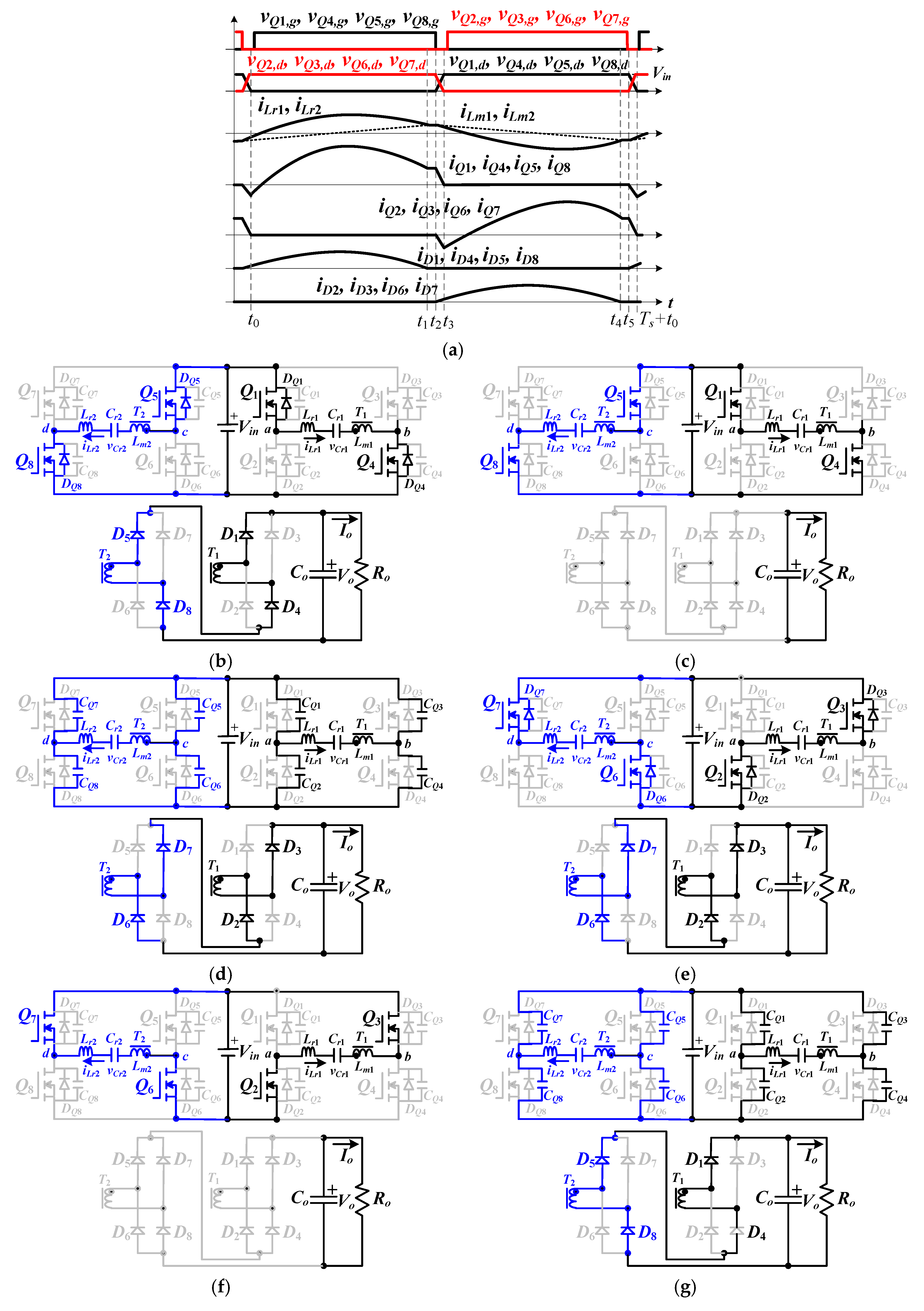
Figure 1a illustrates the presented resonant converter with wide input voltage operation. Two resonant converters are used in the studied circuit with parallel-series connection.
Vin is the input voltage and
Vo is the output voltage.
Lr1 and
Lr2 are resonant inductors,
Cr1 and
Cr2 are resonant capacitors, and
Lm1 and
Lm2 are the magnetizing inductors of transformers
T1 and
T2, respectively. In each resonant circuit, the primary side is a full bridge power converter for medium power rating, and the output side is a full-wave diode rectifier. The passive components (
Cr1 and
Lr1) and (
Cr2 and
Lr2) are naturally resonant in each resonant tank to allow the soft switching on power switches. In low input voltage range
Vin = 100 V ~ 200 V (
Figure 1b), two resonant converters are operated with primary-parallel and secondary-series structure. Each resonant converter provides power
P to output load. Therefore, the total output power is 2
P. Due to the series connection of two diode rectifiers, the load voltage
Vo is the sum of two rectified voltages. Therefore, the voltage rating of diodes
D1 ~
D8 equals
Vo/2. The voltage gain
Geach of each resonant circuit is controlled between 1 and 2. Therefore, the total voltage gain
GTotal of the studied circuit operating at parallel-series connection is regulated at
GTotal = 2 ~ 4 under the low input voltage range from
Vin = 100 V ~ 200 V and
Vo = 400 V. In the high input voltage operation (
Vin = 200 V~400 V) as shown in
Figure 1c, only one resonant converter (
Q1 ~
Q4) is operated, and the other resonant converter (
Q5 ~
Q8) is off. The diodes
D5 ~
D8 are all conducting, and
Vo equals the average rectified voltage of the diode rectifier by
D1 ~
D4. Since the voltage gain of resonant circuit is controlled at
GTotal = 1 ~ 2, the output voltage
Vo can be regulated at 400 V under high input voltage range from
Vin = 200 V ~ 400 V. Based on the circuit structures shown in
Figure 1b,c for low and high voltage input, the wide input voltage operation and the soft switching characteristics are accomplished in the proposed power circuit.
2.1. Under Low Voltage Input Range (Vin = 100 V ~ 200 V)
For low voltage input range, two resonant circuits with parallel-series connection are operated to achieve the higher voltage gain. The dc voltage gain of each resonant converter is controlled between 1 and 2. Since two rectified voltages on the secondary-side are series-connected, the resultant voltage gain of the proposed parallel-series connected resonant converter is regulated between 2 and 4 under 100 V <
Vin < 200 V. The proposed converter has six operating steps in every switching cycle. Under the condition of
fs (switching frequency) >
fr (resonant frequency), the main PWM waveforms are demonstrated in
Figure 2a. The equivalent circuits of six operating steps are provided in
Figure 2b–g.
Step 1 [t0 ~ t1]:D1, D4, D5, and D8 are conducting at t0. Since Q1, Q4, Q5, and Q8 are conducting, the voltages vab = vcd = Vin and vLm1 = vLm2 = nVo, where n is the turns ratio of T1 and T2. Components Cr1 and Lr1 are naturally resonant in the first resonant converter, and components Cr2 and Lr2 are also naturally resonant in the second resonant converter. The resonant frequency .
Step 2 [t1 ~ t2]:Q1, Q4, Q5, and Q8 turn off at time t1. iLr1 and iLr2 are positive. Thus, CQ2, CQ3, CQ6, and CQ7 are discharged, and CQ1, CQ4, CQ5, and CQ8 are charged in this step. Due to iLr1 > iLm1 and iLr2 > iLm2, D1, D4, D5, and D8 are conducting.
Step 3 [t2 ~ t3]: At t2, the voltages of CQ2, CQ3, CQ6, and CQ7 are decreased to zero voltage. Since iLr1 and iLr2 are still positive, DQ2, DQ3, DQ6, and DQ7 conduct. Thus, Q2, Q3, Q6, and Q7 can turn on after t2 with soft switching operation. Since iLr1 > iLm1 and iLr2 > iLm2, diodes D1 and D4 in the first diode rectifier and D5 and D8 in the second diode rectifier are forward biased. Owing to vab = vcd = –Vin and vLm1 = vLm2 = nVo, iLr1 and iLr2 are decreased, and iLm1 and iLm2 are increased.
Step 4 [t3 ~ t4]: At time t3, iLr1 is less than iLm1, and iLr2 is less than iLm2. D2, D3, D6, and D7 are conducting. The magnetizing voltages vLm1 and vLm2 are –nVo so that iLm1 and iLm2 are decreased. Lr1 and Cr1 are naturally resonant with resonant frequency in the first resonant converter. Similarly, Lr2 and Cr2 are naturally resonant in the second resonant converter.
Step 5 [t4 ~ t5]: At t4, switches Q2, Q3, Q6, and Q7 turn off. Owing to iLr1 < 0 and iLr2 < 0, CQ1, CQ4, CQ5, and CQ8 are discharged and CQ2, CQ3, CQ6 and CQ7 are charged in step 5. In this step, iLr1 < iLm1 and iLr2 < iLm2 so that D2, D3, D6, and D7 are conducting.
Step 6 [t5 ~ Ts+t0]: At time t5, the capacitor voltages of CQ1, CQ4, CQ5, and CQ8 are decreased to zero voltage. Owing to iLr1 < 0 and iLr2 < 0, DQ1, DQ4, DQ5, and DQ8 conduct. Therefore, Q1, Q4, Q5, and Q8 turn on after t5 with soft switching operation. Since iLr1 < iLm1 and iLr2 < iLm2, D2, D3, D6, and D7 are still conducting. Owing to vab = vcd = Vin and vLm1 = vLm2 = –nVo, the primary side currents iLr1 and iLr2 are increased, and iLm1 and iLm2 are decreased. At time Ts + t0, iLr1 > iLm1, and iLr2 > iLm2 so that D1, D4, D5, and D8 conduct.
The main PWM waveforms and the equivalent step circuits at low voltage input range under
fs <
fr condition are provided in
Figure 3. Under this condition, the presented circuit has six operation steps in every switching cycle. The circuit operations at
fs <
fr condition are discussed as follows.
Step 1 [t0 ~ t1]:vCQ1 = vCQ4 = vCQ5 = vCQ8 = 0 at time t0. Owing to iLr1(t0) and iLr2(t0) are negative, diodes DQ1, DQ4, DQ5, and DQ8 are conducting. Q1, Q4, Q5, and Q8 can turn on after t0 with soft switching operation. In step 1, vab = vcd = Vin and vLm1 = vLm2 = nVo. Cr1 and Lr1 are naturally resonant in the first resonant tank, and Cr2 and Lr2 are naturally resonant in the second resonant tank.
Step 2 [t1 ~ t2]: Since fs < fr, iLr1 and iLr2 will equal iLm1 and iLm2 at time t1 and D1 ~ D8 are reverse biased. On the primary-side, Lr1, Lm1, and Cr1 are naturally resonant in the first resonant converter and Lr2, Lm2, and Cr2 are naturally resonant in the second resonant converter.
Step 3 [t2 ~ t3]:Q1,
Q4,
Q5, and
Q8 are turned off at time
t2.
CQ2,
CQ3,
CQ6, and
CQ7 are discharged due to
iLr1(
t2) and
iLr2(
t2) are both positive. Since the secondary-side currents of
T1 and
T2 are negative,
D2,
D3,
D6, and
D7 are forward biased. If the energy on
Lr1,
Lr1,
Lm1, and
Lm2 at time
t2 is large enough, then the voltages of
CQ2,
CQ3,
CQ6, and
CQ7 can decrease to zero at time
t3. The soft switching condition of power switches
Q2,
Q3,
Q6, and
Q7 are expressed as.
where
Lm =
Lm1 =
Lm2,
Ce =
CQ1 = ... =
CQ8 and
Lr =
Lr1 =
Lr2.
Step 4 [t3 ~ t4]: At time t3, vCQ2 = vCQ3 = vCQ6 = vCQ7 = 0. Since iLr1(t3) and iLr2(t3) are positive, DQ2, DQ3, DQ6, and DQ7 are conducting. Then Q2, Q3, Q6, and Q7 can turn on after time t3 with zero-voltage switching. In this step, components Cr1 and Lr1 are naturally resonant in the first resonant tank and Cr2 and Lr2 are naturally resonant in the second resonant tank.
Step 5 [t4 ~ t5]: At time t4, iLm1 equals iLr1 and iLm2 equals iLr2. Thus, D1 ~ D8 are all reverse biased. In the first converter, Lr1, Lm1, and Cr1 are resonant, and Lr2, Lm2, and Cr2 are naturally resonant in the second converter with input voltage vab = vcd = –Vin.
Step 6 [t5 ~Ts + t0]:Q2, Q3, Q6, and Q7 turn off at t5. Since iLr1(t5) and iLr2(t5) are negative, CQ1, CQ4, CQ5, and CQ8 are discharged from t5. At time Ts + t0, vCQ1, vCQ4, vCQ5, and vCQ8 are decreased to zero voltage.
2.2. Under High Voltage Input Range (Vin = 200 V ~ 400 V)
For high input voltage case, only one resonant converter (
Q1 ~
Q4) is operated and the other resonant converter (
Q5 ~
Q8) is off. The rectifier diodes
D5 ~
D8 are all conducting and the output voltage of
T1 is connected to the output load (
Figure 1c). The voltage gain of the proposed resonant converter is regulated between 1 and 2 under 200 V <
Vin < 400 V. The proposed converter under high voltage input case has six operating steps for every switching cycle.
Figure 4a gives the PWM waveforms under the condition of
fs >
fr.
Figure 4b–g demonstrate the equivalent circuits of six operating steps. The circuit operations under high input voltage range and
fs >
fr are presented below.
Step 1 [t0 ~ t1]:D1 and D4 are conducting after time t0. Since Q1, Q4, D1, D4, and D5 ~ D8 are conducting, it can obtain the voltages vab = Vin and vLm1 = nVo. Components Cr1 and Lr1 are resonant.
Step 2 [t1 ~ t2]:Q1 and Q4 turn off at t1. Due to iLr1(t1) is positive, CQ2 and CQ3 are charged. Owing to iLr1(t1) > iLm1(t1), D1, D4, and D5 ~ D8 are conducting.
Step 3 [t2 ~ t3]: At time t2, vCQ2 = vCQ3 = 0. Since iLr1(t2) > 0, DQ2 and DQ3 are forward biased and Q2 and Q3 turn on at zero voltage after t2. Since iLr1(t2) > iLm1(t2), D1, D4, and D5 ~ D8 conduct. In this step, vab = –Vin and vLm1 = nVo so that iLr1 decreases and iLm1 increases.
Step 4 [t3 ~ t4]: At t3, iLr1 < iLm1, and D2 and D3 are conducting. In step 4, vLm1 = –nVo and iLm1 decreases. Cr1 and Lr1 are naturally resonant with resonant frequency .
Step 5 [t4 ~ t5]: At t4, Q2 and Q3 are turned off. Since iLr1(t4) < 0, CQ1 and CQ4 are discharged. In this step, iLr1 < iLm1 so that D2, D3, and D6 ~ D8 are conducting.
Step 6 [t5 ~ Ts+t0]: At time t5, vCQ1 = vCQ4 = 0. Since iLr1(t5) < 0, DQ1 and DQ4 are conducting and Q1 and Q4 turn on at zero voltage after t5. Owing to iLr1 < iLm1, D2, D3, and D6 ~ D8 are conducting. In this step, vab = Vin and vLm1 = –nVo so that iLr1 increases and iLm1 decreases. At time Ts+t0, iLr1 > iLm1. Then, D1, D4, and D5 ~ D8 are conducting.
The PWM waveforms under
fs <
fr condition are given in
Figure 5a and the equivalent circuits in every cycle under high voltage input range are provided in
Figure 5b–g. The operation principles under high voltage input and
fs <
fr condition are discussed as follows.
Step 1 [t0 ~ t1]: When t < t0, Q1 ~ Q4 are all off and CQ1 and CQ4 are discharged due to iLr1 < 0. At time t0, vCQ1 = vCQ4 = 0, and DQ1 and DQ4 are conducting. Thus, Q1 and Q4 can turn on after t0 with soft switching operation. The load current flows through the components D1, Co, Ro, D5 ~ D8, and D4 so that the magnetizing inductor voltage vLm1 = nVo and iLm1 increases. Cr1 and Lr1 are naturally resonant with vab = Vin and vLm1 = nVo.
Step 2 [t1 ~ t2]: At t1, iLm1 = iLr1 and D1 ~ D8 are all off. Lr1, Lm1, and Cr1 are naturally resonant with Vab = Vin.
Step 3 [t2 ~ t3]: At t2, Q1, and Q4 turn off. Owing to iLr1(t2) > 0, CQ2 and CQ3 are discharged. Since iLr1 < iLm1 after t2, D2, D3, and D5 ~ D8 conduct.
Step 4 [t3 ~ t4]: At t = t3, vCQ2 = vCQ3 = 0. Since iLr1(t3) is positive, DQ2 and DQ3 are conducting and Q2 and Q3 turn on with zero-voltage switching after time t3. Since Q2, Q3, D2, and D3 are conducting, vab = –Vin and vLm1 = –nVo. Cr1 and Lr1 are naturally resonant with vab = –Vin and vLm1 = –nVo. In step 4, iLr1 and iLm1 both decrease.
Step 5 [t4 ~ t5]: At time t4, iLm1 = iLr1, and D1 ~ D8 are off. Therefore, Lr1, Cr1, and Lm1 are naturally resonant with vab = –Vin.
Step 6 [t5 ~ Ts + t0]:Q2 and Q3 turn off at t5. Owing to iLr1(t5) < 0, CQ1 and CQ4 are discharged. At time Ts + t0, vCQ1 = vCQ4 = 0. Then, the circuit operations in a switching cycle are completed.

