Implementation of a Parallel-Series Resonant Converter with Wide Input Voltage Range


Department. of Electrical Engineering, National Yunlin University of Science and Technology, Yunlin 640, Taiwan
Energies 2019, 12(21), 4095; https://doi.org/10.3390/en12214095
Submission received: 8 October 2019
/
Revised: 22 October 2019
/
Accepted: 25 October 2019
/
Published: 26 October 2019
Abstract
:A new resonant converter is presented to have the advantages of soft switching operation on power devices, without reverse recovery current loss on power diodes and wide input voltage range operation. Resonant converter with frequency modulation is adopted in the proposed circuit to accomplish the low switching loss on power switches and possible zero current switching operation on fast recovery diodes. To improve the problem of limit voltage range operation in the conventional resonant converter, a new parallel-series structure resonant converter is studied to achieve wide input voltage operation capability, such as from Vin,min to 4Vin,min. A 1.8 kW laboratory circuit is implemented, and the measured results are provided to confirm the theoretical analysis and circuit performance.
1. Introduction
Modern power converters with high efficiency and high power density are important to achieve compact size and low power loss. To achieve the low switching loss and compact size, the soft switching circuit topologies with the high switching frequency using wide-band gap power devices, such as GaN power devices, have been developed in modern power electronics. The GaN devices have low switching loss characteristic at high switching frequency, so that the converter efficiency is increased. The main drawback of GaN power devices is high cost compared to power MOSFETs. For the past twenty years, the quasi-resonant (QR) flyback converter [1,2] with low turn-on switching loss, the active clamp dc/dc converters [3] with zero voltage switching operation, the resonant converters [4,5,6] with soft switching operation on power semiconductors, and pulse width modulation (PWM) converters [7,8,9] have been developed to implement high efficiency converters with power MOSFETs devices. QR flyback [1,2] is limited at low power applications, and active clamp dc/dc converters [3] have the problems of dc magnetizing current and unbalance voltage and current stresses on the rectifier diodes. For conventional resonant converters [4,5,6], the input voltage variation is limited due to the limited available voltage gain on the resonant tank. Conventional phase-shift PWM full bridge converters [7,8,9] have drawbacks of hard switching loss at light or low load condition, and high freewheeling current at low load or high input voltage condition. For solar photovoltaic systems, the output voltage of a solar panel is relative to geographical location and solar intensity, so that the solar cell panel has wide output voltage range. Therefore, the power converters with wide voltage operation and high circuit efficiency are demanded for solar power systems. The dc/dc converters with the widespread voltage operation have been proposed in [10,11,12,13,14,15] for fuel cell and solar power converters. In [10,11], the series-connected or parallel-connected structure has been studied to achieve wide input voltage operation on fuel cell power conversion. In [12,13,14,15], the phase-shift PWM dc/dc power converters have been presented to achieve wide voltage operation. In [16], the full-bridge resonant converter with one ac switch and two transformers is proposed to achieve wide input voltage operation. The main drawbacks in [16] are (1) transformer will be shorted suddenly when ac switch is turned on, which will result in serious problems at the transient voltage change and make system unstable, (2) the control scheme of this circuit topology is much more complicated with four equivalent operation topologies, and (3) some power switches will always be conducting at some specific circuit topologies that will increase the conduction loss.
A new parallel-series (full bridge resonant converters are parallel connection and diode rectifiers are series connection) based resonant circuit is developed to obtain the main benefits of the wide input voltage range operation (from vin,min to 4Vin,min) and soft switching operation on power semiconductors. The variable frequency control is used to regulate load voltage over wide input voltage variation. The input impedance of the equivalent resonant tank in the proposed power converter is controlled under the inductive load characteristic. Therefore, the soft switching operation on power semiconductors is achieved. Since two diode rectifiers of the proposed converter are series-connected on the secondary sides, two resonant converters with the parallel-connection on the primary side are worked at the low voltage input (from 100 V to 200 V) to have high dc voltage gain. For high input voltage range (from 200 V to 400 V), only one resonant converter is operated on the primary side to reduce the conduction loss and obtain low dc voltage gain. Therefore, the developed resonant converter can be operated from Vin = 100 V to 400 V. At the low input voltage range, the parallel-series based resonant converter can provide 1.8 kW to output load. At the high input voltage range, only one resonant tank is operated (the other resonant tank is off) to provide 1 kW to output load. The main advantages of the proposed converter compared to [16] are a simple control scheme and low current rating of power switches. At the high input voltage, only four switches instead of eight power switches are operated to reduce power conduction losses. At the low input voltage range, eight power switches are operated to achieve high voltage gain and reduce current rating on each power switch for more power output. The circuit structure, the principle of operation, and design procedure are provided and discussed in this paper. Finally, the experimental waveforms with a 1.8 kW laboratory circuit are presented to show the theoretical examination and investigation of wide input voltage capability.
2. Circuit Diagram and Operating Principle
Figure 1a illustrates the presented resonant converter with wide input voltage operation. Two resonant converters are used in the studied circuit with parallel-series connection. Vin is the input voltage and Vo is the output voltage. Lr1 and Lr2 are resonant inductors, Cr1 and Cr2 are resonant capacitors, and Lm1 and Lm2 are the magnetizing inductors of transformers T1 and T2, respectively. In each resonant circuit, the primary side is a full bridge power converter for medium power rating, and the output side is a full-wave diode rectifier. The passive components (Cr1 and Lr1) and (Cr2 and Lr2) are naturally resonant in each resonant tank to allow the soft switching on power switches. In low input voltage range Vin = 100 V ~ 200 V (Figure 1b), two resonant converters are operated with primary-parallel and secondary-series structure. Each resonant converter provides power P to output load. Therefore, the total output power is 2P. Due to the series connection of two diode rectifiers, the load voltage Vo is the sum of two rectified voltages. Therefore, the voltage rating of diodes D1 ~ D8 equals Vo/2. The voltage gain Geach of each resonant circuit is controlled between 1 and 2. Therefore, the total voltage gain GTotal of the studied circuit operating at parallel-series connection is regulated at GTotal = 2 ~ 4 under the low input voltage range from Vin = 100 V ~ 200 V and Vo = 400 V. In the high input voltage operation (Vin = 200 V~400 V) as shown in Figure 1c, only one resonant converter (Q1 ~ Q4) is operated, and the other resonant converter (Q5 ~ Q8) is off. The diodes D5 ~ D8 are all conducting, and Vo equals the average rectified voltage of the diode rectifier by D1 ~ D4. Since the voltage gain of resonant circuit is controlled at GTotal = 1 ~ 2, the output voltage Vo can be regulated at 400 V under high input voltage range from Vin = 200 V ~ 400 V. Based on the circuit structures shown in Figure 1b,c for low and high voltage input, the wide input voltage operation and the soft switching characteristics are accomplished in the proposed power circuit.
2.1. Under Low Voltage Input Range (Vin = 100 V ~ 200 V)
For low voltage input range, two resonant circuits with parallel-series connection are operated to achieve the higher voltage gain. The dc voltage gain of each resonant converter is controlled between 1 and 2. Since two rectified voltages on the secondary-side are series-connected, the resultant voltage gain of the proposed parallel-series connected resonant converter is regulated between 2 and 4 under 100 V < Vin < 200 V. The proposed converter has six operating steps in every switching cycle. Under the condition of fs (switching frequency) > fr (resonant frequency), the main PWM waveforms are demonstrated in Figure 2a. The equivalent circuits of six operating steps are provided in Figure 2b–g.
Step 1 [t0 ~ t1]:D1, D4, D5, and D8 are conducting at t0. Since Q1, Q4, Q5, and Q8 are conducting, the voltages vab = vcd = Vin and vLm1 = vLm2 = nVo, where n is the turns ratio of T1 and T2. Components Cr1 and Lr1 are naturally resonant in the first resonant converter, and components Cr2 and Lr2 are also naturally resonant in the second resonant converter. The resonant frequency .
Step 2 [t1 ~ t2]:Q1, Q4, Q5, and Q8 turn off at time t1. iLr1 and iLr2 are positive. Thus, CQ2, CQ3, CQ6, and CQ7 are discharged, and CQ1, CQ4, CQ5, and CQ8 are charged in this step. Due to iLr1 > iLm1 and iLr2 > iLm2, D1, D4, D5, and D8 are conducting.
Step 3 [t2 ~ t3]: At t2, the voltages of CQ2, CQ3, CQ6, and CQ7 are decreased to zero voltage. Since iLr1 and iLr2 are still positive, DQ2, DQ3, DQ6, and DQ7 conduct. Thus, Q2, Q3, Q6, and Q7 can turn on after t2 with soft switching operation. Since iLr1 > iLm1 and iLr2 > iLm2, diodes D1 and D4 in the first diode rectifier and D5 and D8 in the second diode rectifier are forward biased. Owing to vab = vcd = –Vin and vLm1 = vLm2 = nVo, iLr1 and iLr2 are decreased, and iLm1 and iLm2 are increased.
Step 4 [t3 ~ t4]: At time t3, iLr1 is less than iLm1, and iLr2 is less than iLm2. D2, D3, D6, and D7 are conducting. The magnetizing voltages vLm1 and vLm2 are –nVo so that iLm1 and iLm2 are decreased. Lr1 and Cr1 are naturally resonant with resonant frequency in the first resonant converter. Similarly, Lr2 and Cr2 are naturally resonant in the second resonant converter.
Step 5 [t4 ~ t5]: At t4, switches Q2, Q3, Q6, and Q7 turn off. Owing to iLr1 < 0 and iLr2 < 0, CQ1, CQ4, CQ5, and CQ8 are discharged and CQ2, CQ3, CQ6 and CQ7 are charged in step 5. In this step, iLr1 < iLm1 and iLr2 < iLm2 so that D2, D3, D6, and D7 are conducting.
Step 6 [t5 ~ Ts+t0]: At time t5, the capacitor voltages of CQ1, CQ4, CQ5, and CQ8 are decreased to zero voltage. Owing to iLr1 < 0 and iLr2 < 0, DQ1, DQ4, DQ5, and DQ8 conduct. Therefore, Q1, Q4, Q5, and Q8 turn on after t5 with soft switching operation. Since iLr1 < iLm1 and iLr2 < iLm2, D2, D3, D6, and D7 are still conducting. Owing to vab = vcd = Vin and vLm1 = vLm2 = –nVo, the primary side currents iLr1 and iLr2 are increased, and iLm1 and iLm2 are decreased. At time Ts + t0, iLr1 > iLm1, and iLr2 > iLm2 so that D1, D4, D5, and D8 conduct.
The main PWM waveforms and the equivalent step circuits at low voltage input range under fs < fr condition are provided in Figure 3. Under this condition, the presented circuit has six operation steps in every switching cycle. The circuit operations at fs < fr condition are discussed as follows.
Step 1 [t0 ~ t1]:vCQ1 = vCQ4 = vCQ5 = vCQ8 = 0 at time t0. Owing to iLr1(t0) and iLr2(t0) are negative, diodes DQ1, DQ4, DQ5, and DQ8 are conducting. Q1, Q4, Q5, and Q8 can turn on after t0 with soft switching operation. In step 1, vab = vcd = Vin and vLm1 = vLm2 = nVo. Cr1 and Lr1 are naturally resonant in the first resonant tank, and Cr2 and Lr2 are naturally resonant in the second resonant tank.
Step 2 [t1 ~ t2]: Since fs < fr, iLr1 and iLr2 will equal iLm1 and iLm2 at time t1 and D1 ~ D8 are reverse biased. On the primary-side, Lr1, Lm1, and Cr1 are naturally resonant in the first resonant converter and Lr2, Lm2, and Cr2 are naturally resonant in the second resonant converter.
Step 3 [t2 ~ t3]:Q1, Q4, Q5, and Q8 are turned off at time t2. CQ2, CQ3, CQ6, and CQ7 are discharged due to iLr1(t2) and iLr2(t2) are both positive. Since the secondary-side currents of T1 and T2 are negative, D2, D3, D6, and D7 are forward biased. If the energy on Lr1, Lr1, Lm1, and Lm2 at time t2 is large enough, then the voltages of CQ2, CQ3, CQ6, and CQ7 can decrease to zero at time t3. The soft switching condition of power switches Q2, Q3, Q6, and Q7 are expressed as.
where Lm = Lm1 = Lm2, Ce = CQ1 = ... = CQ8 and Lr = Lr1 = Lr2.
Step 4 [t3 ~ t4]: At time t3, vCQ2 = vCQ3 = vCQ6 = vCQ7 = 0. Since iLr1(t3) and iLr2(t3) are positive, DQ2, DQ3, DQ6, and DQ7 are conducting. Then Q2, Q3, Q6, and Q7 can turn on after time t3 with zero-voltage switching. In this step, components Cr1 and Lr1 are naturally resonant in the first resonant tank and Cr2 and Lr2 are naturally resonant in the second resonant tank.
Step 5 [t4 ~ t5]: At time t4, iLm1 equals iLr1 and iLm2 equals iLr2. Thus, D1 ~ D8 are all reverse biased. In the first converter, Lr1, Lm1, and Cr1 are resonant, and Lr2, Lm2, and Cr2 are naturally resonant in the second converter with input voltage vab = vcd = –Vin.
Step 6 [t5 ~Ts + t0]:Q2, Q3, Q6, and Q7 turn off at t5. Since iLr1(t5) and iLr2(t5) are negative, CQ1, CQ4, CQ5, and CQ8 are discharged from t5. At time Ts + t0, vCQ1, vCQ4, vCQ5, and vCQ8 are decreased to zero voltage.
2.2. Under High Voltage Input Range (Vin = 200 V ~ 400 V)
For high input voltage case, only one resonant converter (Q1 ~ Q4) is operated and the other resonant converter (Q5 ~ Q8) is off. The rectifier diodes D5 ~ D8 are all conducting and the output voltage of T1 is connected to the output load (Figure 1c). The voltage gain of the proposed resonant converter is regulated between 1 and 2 under 200 V < Vin < 400 V. The proposed converter under high voltage input case has six operating steps for every switching cycle. Figure 4a gives the PWM waveforms under the condition of fs > fr. Figure 4b–g demonstrate the equivalent circuits of six operating steps. The circuit operations under high input voltage range and fs > fr are presented below.
Step 1 [t0 ~ t1]:D1 and D4 are conducting after time t0. Since Q1, Q4, D1, D4, and D5 ~ D8 are conducting, it can obtain the voltages vab = Vin and vLm1 = nVo. Components Cr1 and Lr1 are resonant.
Step 2 [t1 ~ t2]:Q1 and Q4 turn off at t1. Due to iLr1(t1) is positive, CQ2 and CQ3 are charged. Owing to iLr1(t1) > iLm1(t1), D1, D4, and D5 ~ D8 are conducting.
Step 3 [t2 ~ t3]: At time t2, vCQ2 = vCQ3 = 0. Since iLr1(t2) > 0, DQ2 and DQ3 are forward biased and Q2 and Q3 turn on at zero voltage after t2. Since iLr1(t2) > iLm1(t2), D1, D4, and D5 ~ D8 conduct. In this step, vab = –Vin and vLm1 = nVo so that iLr1 decreases and iLm1 increases.
Step 4 [t3 ~ t4]: At t3, iLr1 < iLm1, and D2 and D3 are conducting. In step 4, vLm1 = –nVo and iLm1 decreases. Cr1 and Lr1 are naturally resonant with resonant frequency .
Step 5 [t4 ~ t5]: At t4, Q2 and Q3 are turned off. Since iLr1(t4) < 0, CQ1 and CQ4 are discharged. In this step, iLr1 < iLm1 so that D2, D3, and D6 ~ D8 are conducting.
Step 6 [t5 ~ Ts+t0]: At time t5, vCQ1 = vCQ4 = 0. Since iLr1(t5) < 0, DQ1 and DQ4 are conducting and Q1 and Q4 turn on at zero voltage after t5. Owing to iLr1 < iLm1, D2, D3, and D6 ~ D8 are conducting. In this step, vab = Vin and vLm1 = –nVo so that iLr1 increases and iLm1 decreases. At time Ts+t0, iLr1 > iLm1. Then, D1, D4, and D5 ~ D8 are conducting.
The PWM waveforms under fs < fr condition are given in Figure 5a and the equivalent circuits in every cycle under high voltage input range are provided in Figure 5b–g. The operation principles under high voltage input and fs < fr condition are discussed as follows.
Step 1 [t0 ~ t1]: When t < t0, Q1 ~ Q4 are all off and CQ1 and CQ4 are discharged due to iLr1 < 0. At time t0, vCQ1 = vCQ4 = 0, and DQ1 and DQ4 are conducting. Thus, Q1 and Q4 can turn on after t0 with soft switching operation. The load current flows through the components D1, Co, Ro, D5 ~ D8, and D4 so that the magnetizing inductor voltage vLm1 = nVo and iLm1 increases. Cr1 and Lr1 are naturally resonant with vab = Vin and vLm1 = nVo.
Step 2 [t1 ~ t2]: At t1, iLm1 = iLr1 and D1 ~ D8 are all off. Lr1, Lm1, and Cr1 are naturally resonant with Vab = Vin.
Step 3 [t2 ~ t3]: At t2, Q1, and Q4 turn off. Owing to iLr1(t2) > 0, CQ2 and CQ3 are discharged. Since iLr1 < iLm1 after t2, D2, D3, and D5 ~ D8 conduct.
Step 4 [t3 ~ t4]: At t = t3, vCQ2 = vCQ3 = 0. Since iLr1(t3) is positive, DQ2 and DQ3 are conducting and Q2 and Q3 turn on with zero-voltage switching after time t3. Since Q2, Q3, D2, and D3 are conducting, vab = –Vin and vLm1 = –nVo. Cr1 and Lr1 are naturally resonant with vab = –Vin and vLm1 = –nVo. In step 4, iLr1 and iLm1 both decrease.
Step 5 [t4 ~ t5]: At time t4, iLm1 = iLr1, and D1 ~ D8 are off. Therefore, Lr1, Cr1, and Lm1 are naturally resonant with vab = –Vin.
Step 6 [t5 ~ Ts + t0]:Q2 and Q3 turn off at t5. Owing to iLr1(t5) < 0, CQ1 and CQ4 are discharged. At time Ts + t0, vCQ1 = vCQ4 = 0. Then, the circuit operations in a switching cycle are completed.
3. Circuit Analysis and Design Procedures
Variable frequency control is used to generate the PWM signals of power switches and regulate output voltage at Vo = 400 V under wide voltage variation from Vin = 100 V to 400 V. Then, a dc/ac inverter can be adopted as the second stage for PV inverter applications. The fundamental harmonic analysis is adopted to derive the voltage transfer function of the proposed converter. For low voltage input range from Vin = 100V to 200V, two resonant converters are operated, and the output voltages of two diode rectifiers are series connection to achieve high voltage gain (Figure 1b). For high voltage input range from Vin = 200 V to 400 V, only one resonant converter is operated on the primary side to regulate load voltage (Figure 1c). Since the frequency modulation is used in the presented circuit, it can obtain that the waveforms on vab and vcd are square voltage waveforms. Based on the Fourier Series Analysis (FSA), the fundamental root-mean-square (rms) voltages Vab,rms and Vcd,rms are obtained as.
For low input voltage range (Vin = 100 V ~ 200 V), the magnetizing voltages vLm1 = vLm2 = ±nVo/2. On the other hand, the magnetizing voltage vLm1 = ±nVo and vLm2 = 0 for high input voltage range (Vin = 200 V ~ 400 V). Therefore, the fundamental rms magnetizing voltages are derived as.
According to the dc load resistor Ro, the equivalent ac resistors Rac1 and Rac2 on the primary-side of T1 and T2 can be obtained as:
According to the resonant components Lr1, Cr1, Rac1, and Lm1, the voltage gain of the presented resonant converter is derived in (8).
where is the quality factor, ln = Lm1/Lr1 is the inductor ratio, and fn = fs/fr is the frequency ratio. The output voltage can be obtained in (9).
According to the input and output voltage conditions, the switching frequency of power switches Q1 ~ Q8 are regulated according to the input voltage variation. Since the input impedance of the proposed resonant circuit is controlled at the inductive load, Q1 ~ Q8 can be turned on under zero voltage switching. The power loss analysis of the resonant converter or inverters has been discussed in [17,18] for fixed switching frequency. However, the switching frequency of the resonant converter is variable. Therefore, it is very difficult to predict and calculate the actual power losses. In the proposed converter, the main power losses are conduction losses on power switches Q1 ~ Q8, copper and core losses on the resonant inductors Lr1 and Lr2 and transformers T1 and T2, conduction losses on the resonant capacitors Cr1 and Cr2, and the conduction losses on the rectifier diodes Q1 ~ Q8. The rms currents of the resonant capacitors Cr1 and Cr2 at the series resonant frequency are calculated as:
It is clear that the primary currents are related to the switching frequency fsw and the magnetizing voltage VLm1. In the same input voltage range such as Vin = 100 V ~ 200 V, the low input voltage (Vin = 100 V) will result in low switching frequency. The low switching frequency will increase the primary current and conduction loss on power switches, inductors, and resonant capacitors. Therefore, the proposed converter efficiency at Vin = 100 V is less than the efficiency at Vin = 200 V. For low input voltage range (Vin = 100 V ~ 200 V), two resonant circuits are operated, and the magnetizing voltages VLm1 = VLm2 = nVo/2 instead of VLm1 = nVo under high input voltage range (Vin = 200 V ~ 400 V). Therefore, the circuit efficiency operated at low input voltage range is better than the circuit efficiency operated at high input voltage range.
To confirm the theoretical analysis, a design example of a laboratory circuit is provided with the electric specifications Vin = 100 V ~ 400 V and Vo = 400 V. The rated power is 1800 W (by two resonant circuits) for low input voltage range and 1 kW (by one resonant circuit) for high input voltage range. The series resonant frequency of the resonant tank is designed at 100 kHz. For low input voltage range Vin = 100 V ~ 200 V, two resonant circuits with parallel-series connection are operated in the studied circuit to obtain high voltage gain. However, one only resonant circuit is operated under high voltage input Vin = 200 V ~ 400 V. Figure 6 provides the voltage gain of the studied converter with wide input voltage operation. The transient voltage (Vin,tran) between low input voltage range and high input voltage range is selected at 200 V with ±4 V voltage tolerance. From equation (8), it is clear that the voltage gain of the presented resonant converter under high input voltage range is two times of voltage gain under low input voltage range. Therefore, the design considerations for two resonant converters operation (Figure 1b) for low voltage input and one resonant converter operation (Figure 1c) for high voltage input are identical. To simplify the design consideration, only one resonant converter under high voltage range is discussed to design circuit components. Under high voltage range, the minimum voltage gain Gmin is designed as unity at Vin,max = 400 V. From equation (8), the turn-ratio n1 is obtained as:
Magnetic cores EE-55 with flux density ΔB = 0.4 tesla and window area Ae = 3.54 cm2 are used to build the isolated transformers T1 and T2. The minimum switching frequency of the resonant converter is designed at 55 kHz and 200 V input. Therefore, the minimum primary turns at 200 V input are calculated as:
The actual primary turns and secondary turns of transformers T1 and T2 are Np1 = Np2 = Ns1 = Ns2 = 52 turns. From equation (6), the equivalent resistance Rac1 under Po = 1 kW and Vo = 400 V is obtained as:
The selected inductor ratio ln is equal to 5, and the selected quality factor x is equal to 0.2. Based on the ln, Rac1, x, and fr, the theoretical resonant components are derived as:
In the prototype circuit, the actual resonant components are Lr1 = Lr2 = 40 μH, Lm1 = Lm2 = 200 μH and Cr1 = Cr2 = 63 nF. The voltage stress of Q1 ~ Q8 equals Vin,max = 400 V and power MOSFETs STW48N60M2 with 600 V/26 A rating are used for Q1 ~ Q8. The voltage stress of D1 ~ D8 equals Vo = 400 V and STTH8R06FP with 600 V/8 A are used for D1 ~ D8. The selected output capacitance Co = 810 μF (three 270 μF in parallel).
4. Test Results
Experiments based on a prototype circuit shown in Figure 7 are demonstrated to confirm the circuit performance. The test results at low input voltage range are shown in Figure 8 and Figure 9 with Vin = 100 V and 190 V, respectively. For low voltage range, two resonant circuits are operated with parallel-input and series-output structure to achieve high voltage gain. Figure 8 are the test waveforms under Vin = 100 V, Vo = 400 V and Po = 1.8 kW. Figure 8a provides the measured waveforms of vQ1,g ~ vQ8,g. The test switching frequency at Vin = 100 V shown in Figure 8a is about 51 kHz. Figure 8b gives the experimental waveforms of the resonant currents and voltages. Due to fs (51 kHz) < fr (100 kHz), the resonant currents iLr1 and iLr2 are quasi-sinusoidal waveforms. Figure 8c,d provide the current waveforms of the rectifier diodes. Owing to fs < fr, the rectifier diodes D1 ~ D8 are all reverse biased without reverse recovery current loss. Figure 8e demonstrates the experimental waveforms under Vin = 100 V, Vo = 400 V and Io = 4.5 A (Po = 1.8 kW). Figure 8f demonstrates the experimental waveforms of power switch Q1 at full load. Before Q1 turns on, the drain voltage vQ1,d is already zero voltage. Therefore, the zero voltage turn-on of Q1 is achieved. Q2 ~ Q8 have the same turn-on characteristic as Q1 with soft switching operation. Figure 9 provides the test waveform under Vin = 190 V, Vo = 400 V and Po = 1.8 kW. The switch signals of Q1 ~ Q8 are provided in Figure 9a. The measured resonant current and voltages are given in Figure 9b. Since fs ≈ fr, the resonant currents are sinusoidal waveforms. The measured diode currents are provided in Figure 9c,d. The measured waveforms of input voltage Vin = 190 V, load voltage Vo = 400 V and load current Io = 4.5 A are provided in Figure 9e. The test waveforms of switch Q1 are given in Figure 9f. For high input voltage range, Figure 10 and Figure 11 shows the experimental results of the studied circuit at Vin = 210 V and 400 V, respectively. For high input voltage range, only one resonant converter (Q1 ~ Q4) is controlled to regulate load voltage. The rectifier diodes D5 ~ D8 are bypassed at high voltage range operation. The measured waveforms at Vin = 210 V, Vo = 400 V and Po = 1 kW are provided in Figure 10. Due to the voltage gain at Vin = 210 V is close to 2 (under high input voltage range), it is obtained that fs < fr. From Figure 10b, the resonant current iLr1 is a quais-sinusoidal waveform. From Figure 10c,d, D1 ~ D8 turn off under zero current switching. Since the diodes D5 ~ D8 are bypassed for high input voltage range, the secondary-side rectified current is distributed on D5 ~ D8. Therefore, the diode currents iD5 ~ iD8 are balanced and the amplitude of iD5 ~ iD8 is only one-half of amplitude of iD1 ~ iD4. From test results in Figure 10f, it can observe that the soft switching turn-on of Q1 is achieved. Figure 11 provides the test waveforms under Vin = 400 V, Vo = 400 V and Po = 1 kW. The voltage gain at Vin = 400 V is 1 (Figure 6). The resonant current iLr1 is a sinusoidal waveform (Figure 11b). Similarly, the secondary-side rectified current is distributed on D5 ~ D8 and the amplitude of iD5 ~ iD8 (Figure 11d) is equal to one-half of amplitude of iD1 ~ iD4 (Figure 11c). From the experimental waveforms in Figure 11f, Q1 is turned on at zero voltage switching. The measured circuit efficiencies of the proposed converter are 92.55% at Vin = 100 V and Po = 1.8 kW, 94.1% at Vin = 190 V and Po = 1.8 kW, 90.8% at Vin = 210 V and Po = 1 kW, and 91.8% at Vin = 400 V and Po = 1 kW. It is clear that the proposed converter has better circuit efficiency at low input voltage case. Because the magnetizing current loss is depended on the output voltage instead of input voltage. For high voltage input, only one resonant converter is operated to provide 1 kW output. However, 1.8 kW is provided by two resonant converters at low voltage input case. Therefore, the proposed converter has better circuit efficiency at low input voltage case. Figure 12 provides the test circuit efficiencies of the proposed resonant converter for 50% and 100% rated power under different input voltages.
5. Conclusions
A new resonant converter is proposed, discussed, and implemented to have low switching losses on power devices and wide input voltage operation from Vin = 100 V to 400 V. To overcome the drawback of the limit range of input voltage operation on conventional resonant converter, two resonant circuits with parallel-series connection are used in the proposed converter. For low voltage input, the output voltages of two diode rectifiers are series-connected to have higher voltage gain. On the other hand, only one resonant circuit is operated and the other circuit is off under high input voltage range. Because the presented resonant circuit is operated at the inductive input impedance, the soft switching operation of all active devices is achieved. The proposed resonant converter can be implemented by the general integrated circuit with the frequency modulation and a voltage comparator. The applications of the studied circuit are front stage of solar power conversion with wide input voltage variation and high voltage output. Although two independent resonant converters working for each voltage range can also be adopted to achieve wide input voltage operation, the current rating of active and passive power components in the proposed converter is much lower (half current rating) than two converters working for low input voltage case. Finally, a 1.8 kW laboratory circuit was constructed and measured. Experiments are demonstrated to confirm the circuit performance and usefulness of the studied resonant converter with wide voltage range capability.
Author Contributions
B.-R.L. proposed and designed this project and was responsible for writing the paper.
Funding
This research is funded by the Ministry of Science and Technology, Taiwan, under grant number MOST 108-2221-E-224-022-MY2.
Acknowledgments
This research is supported by the Ministry of Science and Technology, Taiwan, under contract MOST 108-2221-E-224-022-MY2. The author would like to thank H. R. Cheng for his help to measure the circuit waveforms in the experiment.
Conflicts of Interest
The author declares no conflict of interest.
References
- Wang, Y.; Zhang, S.; Guan, Y.; Liu, X.; Xu, D. Single-stage QR ac-dc converter based on buck-boost and flyback circuits. IET Power Electron. 2017, 10, 103–111. [Google Scholar] [CrossRef]
- Xie, X.; Li, J.; Peng, K.; Zhao, C.; Lu, Q. Study on the single-stage forward-flyback PFC converter with QR control. IEEE Trans. Power Electron. 2016, 31, 430–442. [Google Scholar] [CrossRef]
- Lin, B.R.; Chiang, H.K.; Chen, C.C. Analysis and implementation of a ZVS-PWM converter with series-connected transformers. IEEE Trans. Circuits Syst. Part II Express Briefs 2007, 54, 917–921. [Google Scholar] [CrossRef]
- Singh, A.K.; Das, P.; Panda, S.K. Analysis and design of SQR-based high-voltage LLC resonant DC-DC converter. IEEE Trans. Power Electron. 2017, 32, 4466–4481. [Google Scholar] [CrossRef]
- Haga, H.; Kurokawa, F. Modulation method of a full-bridge three-level LLC resonant converter for battery charger of electric vehicles. IEEE Trans. Power Electron. 2017, 32, 2498–2507. [Google Scholar] [CrossRef]
- Lin, B.R.; Lin, Y. Parallel current-fed resonant converter with balance current sharing and no input ripple current. IET Power Electron 2019, 12, 212–219. [Google Scholar] [CrossRef]
- Safaee, A.; Jain, P.; Bakhshai, A. A ZVS pulsewidth modulation full-bridge converter with a low-RMS-current resonant auxiliary circuit. IEEE Trans. Power Electron. 2016, 31, 4031–4047. [Google Scholar] [CrossRef]
- Liu, P.J.; Hsu, Y.C.; Hsu, S.R. Drain-voltage balance and phase-shifted PWM control schemes for high-efficiency parallel-string dimmable LED drivers. IEEE Trans. Ind. Electron. 2018, 65, 6168–6176. [Google Scholar] [CrossRef]
- Mishima, T.; Akamatsu, K.; Nakaoka, M. A high frequency-link secondary-side phase-shifted full-bridge soft-switching PWM DC-DC converter with ZCS active rectifier for EV battery charged. IEEE Trans. Power Electron. 2013, 28, 5758–5773. [Google Scholar] [CrossRef]
- Zhang, Y.; Fu, C.; Sumner, M.; Wang, P. A wide input-voltage range quasi-Z-source boost DC–DC converter with high-voltage gain for fuel cell vehicles. IEEE Trans. Ind. Electron. 2018, 65, 5201–5212. [Google Scholar] [CrossRef]
- Yao, Z.; Xu, J. A three-phase DC-DC converter for low and wide input-voltage range application. In Proceedings of the 2016 IEEE Transportation Electrification Conference and Expo, Asia-Pacific (ITEC Asia-Pacific), Busan, Korea, 1–4 June 2016; pp. 208–213. [Google Scholar]
- Li, W.; Zong, S.; Liu, F.; Yang, H.; He, X.; Wu, B. Secondary-side phase-shift-controlled ZVS DC/DC converter with wide voltage gain for high input voltage applications. IEEE Trans. Power Electron. 2013, 28, 5128–5139. [Google Scholar] [CrossRef]
- Wang, X.; Tian, F.; Batarseh, I. High efficiency parallel post regulator for wide range input DC–DC converter. IEEE Trans. Power Electron. 2008, 23, 852–858. [Google Scholar] [CrossRef]
- Lu, J.; Kumar, A.; Afridi, K.K. Step-down impedance control network resonant DC-DC converter utilizing an enhanced phase-shift control for wide-input-range operation. IEEE Trans. Ind. Applica. 2018, 54, 4523–4536. [Google Scholar] [CrossRef]
- Wu, H.; Wan, C.; Sun, K.; Xing, Y. A high step-down multiple output converter with wide input voltage range based on quasi two-stage architecture and dual-output LLC resonant converter. IEEE Trans. Power Electron. 2015, 30, 1793–1796. [Google Scholar] [CrossRef]
- Hu, H.; Fang, X.; Chen, F.; Shen, Z.J.; Batarseh, I. A modified high-efficiency LLC converter with two transformers for wide input-voltage range applications. IEEE Trans. Power Electron. 2012, 28, 1946–1960. [Google Scholar] [CrossRef]
- Albertoni, L.; Grasso, F.; Matteucci, J.; Piccirilli, M.C.; Reatti, A.; Ayachit, A.; Kazimierczuk, M.K. Analysis and design of full-bridge Class-DE inverter at fixed duty cycle. In Proceedings of the IECON 2016-42nd Annual Conference of the IEEE Industrial Electronics Society, Florence, Italy, 23–26 October 2016; pp. 5609–5614. [Google Scholar]
- Ayachit, A.; Corti, F.; Reatti, A.; Kazimierczuk, M.K. Zero-voltage switching operation of transformer class-E inverter at any coupling coefficient. IEEE Trans. Ind. Electron. 2019, 66, 1809–1819. [Google Scholar] [CrossRef]
Figure 1.
Circuit configurations of the developed dc/dc converter: (a) The proposed circuit structure; (b) at low voltage input range; (c) at high voltage input range.
Figure 1.
Circuit configurations of the developed dc/dc converter: (a) The proposed circuit structure; (b) at low voltage input range; (c) at high voltage input range.

Figure 2.
Circuit waveforms and equivalent circuits at low input voltage range and fs > fr, (a) PWM waveforms, (b) step 1, (c) step 2, (d) step 3, (e) step 4, (f) step 5, (g) step 6.
Figure 2.
Circuit waveforms and equivalent circuits at low input voltage range and fs > fr, (a) PWM waveforms, (b) step 1, (c) step 2, (d) step 3, (e) step 4, (f) step 5, (g) step 6.


Figure 3.
Circuit waveforms and equivalent circuits at low input voltage range and fs < fr, (a) PWM waveforms, (b) step 1, (c) step 2, (d) step 3, (e) step 4, (f) step 5, (g) step 6.
Figure 3.
Circuit waveforms and equivalent circuits at low input voltage range and fs < fr, (a) PWM waveforms, (b) step 1, (c) step 2, (d) step 3, (e) step 4, (f) step 5, (g) step 6.
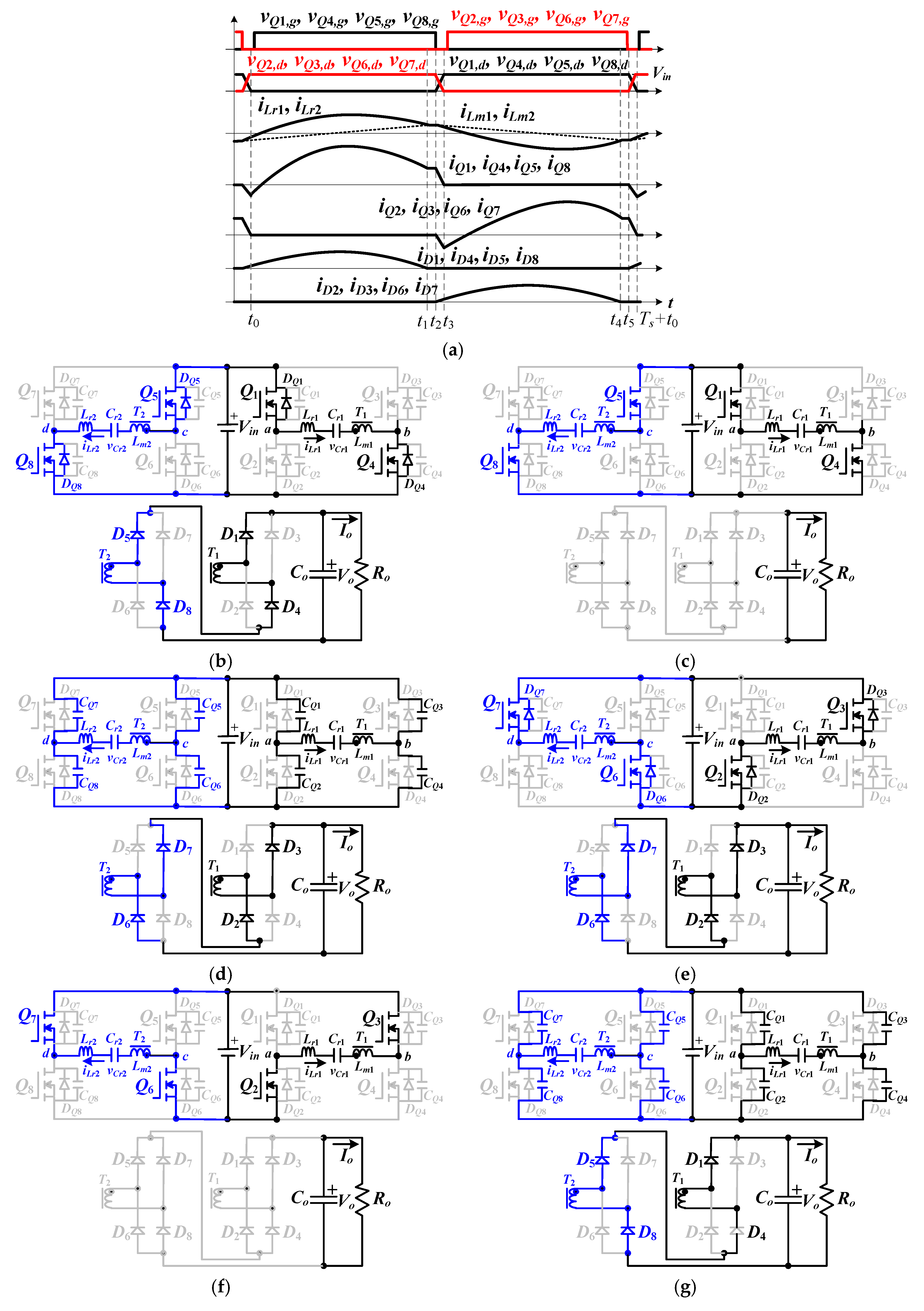
Figure 4.
Circuit waveforms and equivalent circuits at high input voltage range and fs > fr, (a) PWM waveforms, (b) step 1, (c) step 2, (d) step 3, (e) step 4, (f) step 5, (g) step 6.
Figure 4.
Circuit waveforms and equivalent circuits at high input voltage range and fs > fr, (a) PWM waveforms, (b) step 1, (c) step 2, (d) step 3, (e) step 4, (f) step 5, (g) step 6.


Figure 5.
Circuit waveforms and equivalent circuits at high input voltage range and fs < fr, (a) PWM waveforms, (b) step 1, (c) step 2, (d) step 3, (e) step 4, (f) step 5, (g) step 6.
Figure 5.
Circuit waveforms and equivalent circuits at high input voltage range and fs < fr, (a) PWM waveforms, (b) step 1, (c) step 2, (d) step 3, (e) step 4, (f) step 5, (g) step 6.

Figure 6.
Voltage gain of the studied circuit for Vin 100 V ~ 400 V and Vo = 400 V.

Figure 7.
Picture of the laboratory prototype circuit.

Figure 8.
Experimental results at Vin = 100 V (low voltage range) and 1.8 kW load. (a) vQ1,g ~ vQ8,g, (b) vCr1, iLr1, vCr2, iLr2, (c) iD1 ~ iD4, (d) iD5 ~ iD8, (e) Vin, Vo, Io, (f) vQ1,g, vQ1,d, iQ1.
Figure 8.
Experimental results at Vin = 100 V (low voltage range) and 1.8 kW load. (a) vQ1,g ~ vQ8,g, (b) vCr1, iLr1, vCr2, iLr2, (c) iD1 ~ iD4, (d) iD5 ~ iD8, (e) Vin, Vo, Io, (f) vQ1,g, vQ1,d, iQ1.

Figure 9.
Experimental results at Vin = 190 V (low voltage range) and 1.8 kW load. (a) vQ1,g ~ vQ8,g, (b) vCr1, iLr1, vCr2, iLr2, (c) iD1 ~ iD4, (d) iD5 ~ iD8, (e) Vin, Vo, Io, (f) vQ1,g, vQ1,d, iQ1.
Figure 9.
Experimental results at Vin = 190 V (low voltage range) and 1.8 kW load. (a) vQ1,g ~ vQ8,g, (b) vCr1, iLr1, vCr2, iLr2, (c) iD1 ~ iD4, (d) iD5 ~ iD8, (e) Vin, Vo, Io, (f) vQ1,g, vQ1,d, iQ1.


Figure 10.
Experimental waveforms at Vin = 210 V (high voltage range) and 1 kW load. (a) vQ1,g ~ vQ4,g, (b) vab, vCr1, iLr1, (c) iD1 ~ iD4, (d) iD5 ~ iD8, (e) Vin, Vo, Io, (f) vQ1,g, vQ1,d, iQ1.
Figure 10.
Experimental waveforms at Vin = 210 V (high voltage range) and 1 kW load. (a) vQ1,g ~ vQ4,g, (b) vab, vCr1, iLr1, (c) iD1 ~ iD4, (d) iD5 ~ iD8, (e) Vin, Vo, Io, (f) vQ1,g, vQ1,d, iQ1.


Figure 11.
Experimental results at Vin = 400 V (high voltage range) and 1 kW load. (a) vQ1,g ~ vQ4,g, (b) vab, vCr1, iLr1, (c) iD1 ~ iD4, (d) iD5 ~ iD8, (e) Vin, Vo, Io, (f) vQ1,g, vQ1,d, iQ1.
Figure 11.
Experimental results at Vin = 400 V (high voltage range) and 1 kW load. (a) vQ1,g ~ vQ4,g, (b) vab, vCr1, iLr1, (c) iD1 ~ iD4, (d) iD5 ~ iD8, (e) Vin, Vo, Io, (f) vQ1,g, vQ1,d, iQ1.


Figure 12.
Measured efficiencies of the proposed circuit for 50% and 100% rated power under different input voltages. (a) low input voltage range, (b) high input voltage range.
Figure 12.
Measured efficiencies of the proposed circuit for 50% and 100% rated power under different input voltages. (a) low input voltage range, (b) high input voltage range.

© 2019 by the author. Licensee MDPI, Basel, Switzerland. This article is an open access article distributed under the terms and conditions of the Creative Commons Attribution (CC BY) license (http://creativecommons.org/licenses/by/4.0/).
Share and Cite
MDPI and ACS Style
Lin, B.-R. Implementation of a Parallel-Series Resonant Converter with Wide Input Voltage Range. Energies 2019, 12, 4095. https://doi.org/10.3390/en12214095
AMA Style
Lin B-R. Implementation of a Parallel-Series Resonant Converter with Wide Input Voltage Range. Energies. 2019; 12(21):4095. https://doi.org/10.3390/en12214095
Chicago/Turabian StyleLin, Bor-Ren. 2019. "Implementation of a Parallel-Series Resonant Converter with Wide Input Voltage Range" Energies 12, no. 21: 4095. https://doi.org/10.3390/en12214095
Note that from the first issue of 2016, this journal uses article numbers instead of page numbers. See further details here.