Simple DC-Link Voltage Balancing Approach for Cascaded H-Bridge Rectifier with Asymmetric Parameters of Independent DC Loads

Abstract
:1. Introduction
2. Configuration of Cascaded Module Structure
3. PD-PWM Method
3.1. PD-PWM Used in Cascaded Chopper Structure
3.2. Conventional PD-PWM Used in Cascaded H-Bridge Structure
3.3. Dual Modulation Signal Based PD-PWM Used in Cascaded H-Bridge Structure
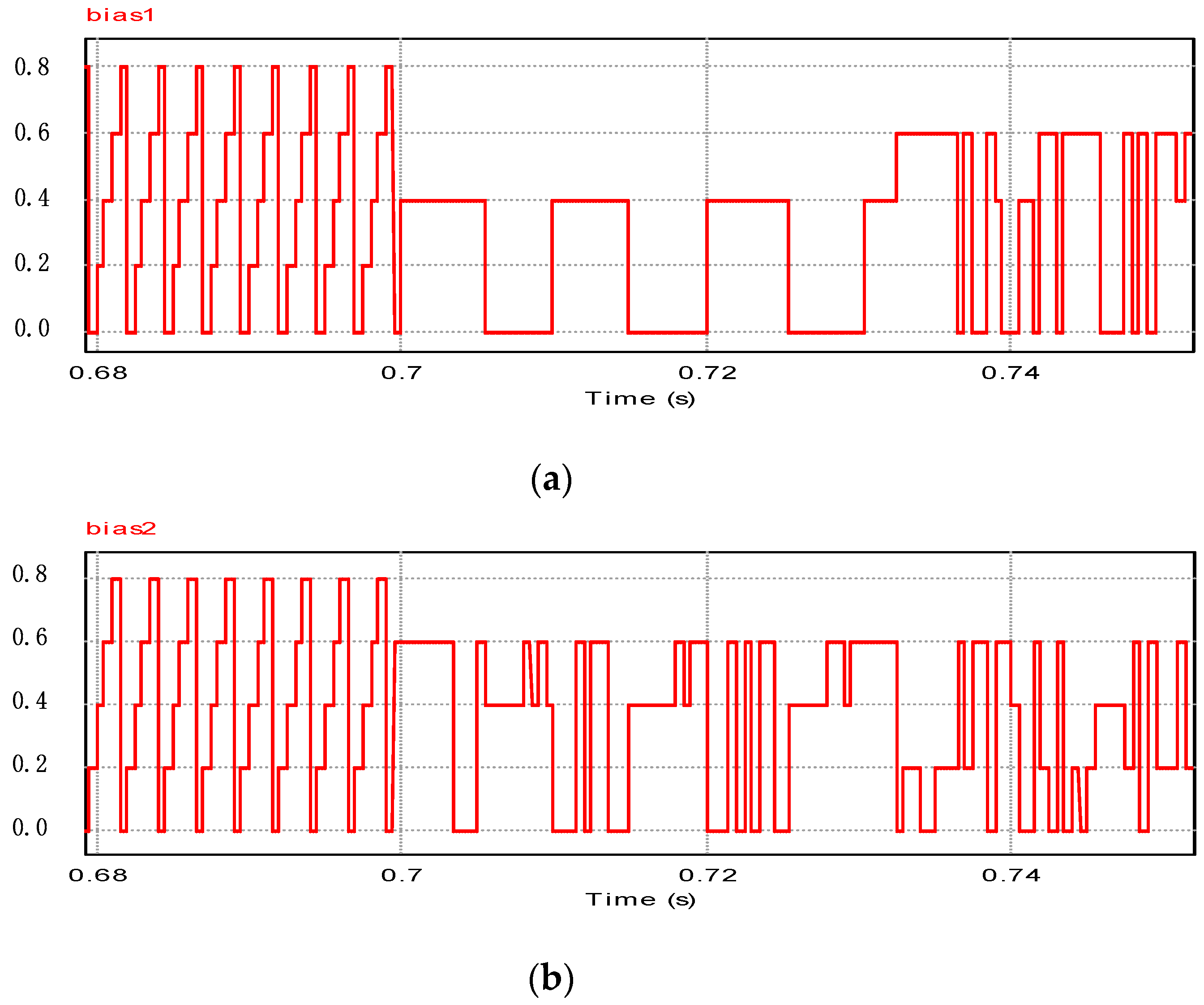
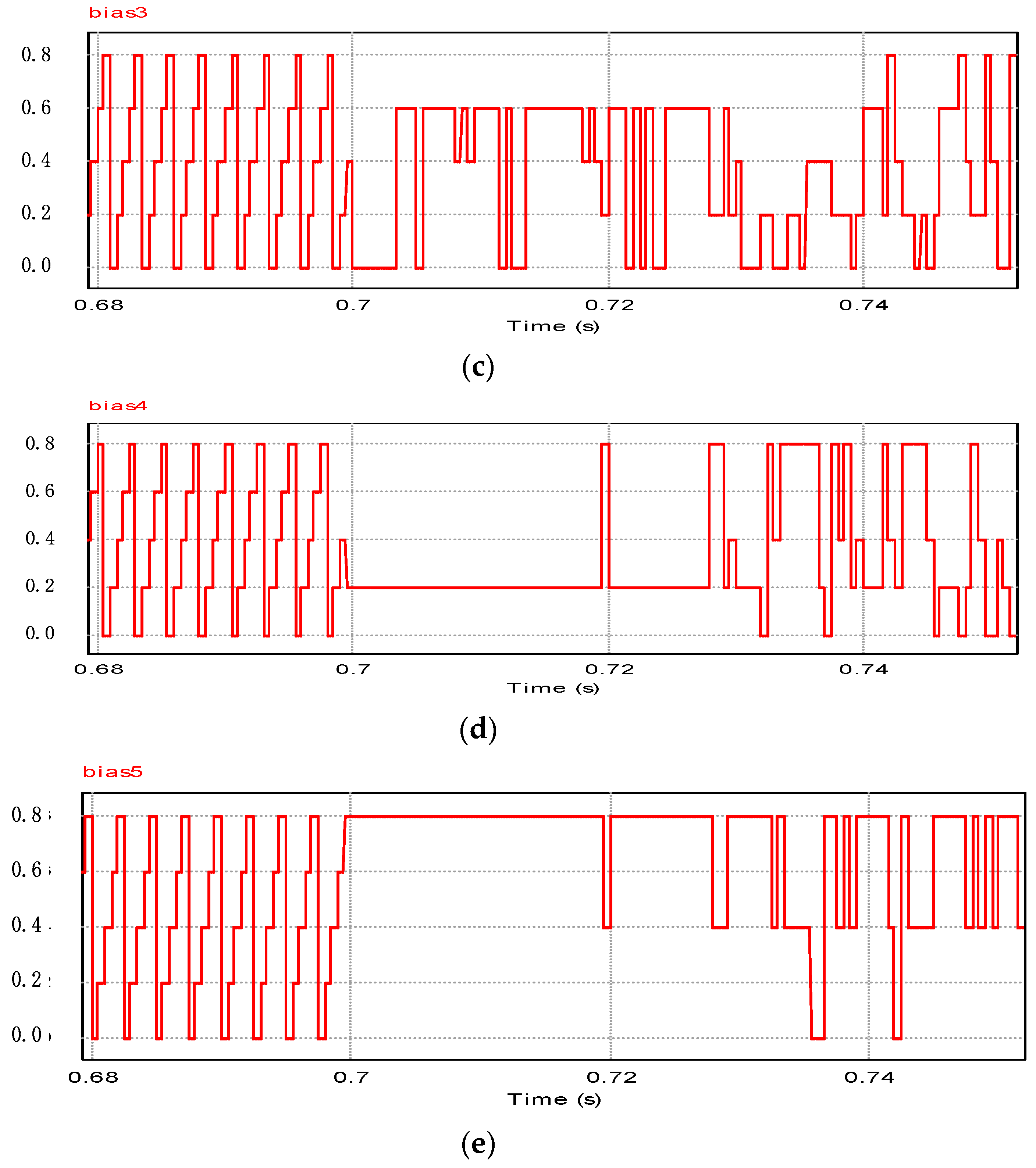
4. Dynamic Carrier Bias Allocation Strategy Based on Operation Condition
4.1. Charge-Discharge Law of Dual Modulation Signal Based PD-PWM Used in CHB Structure
- (1)
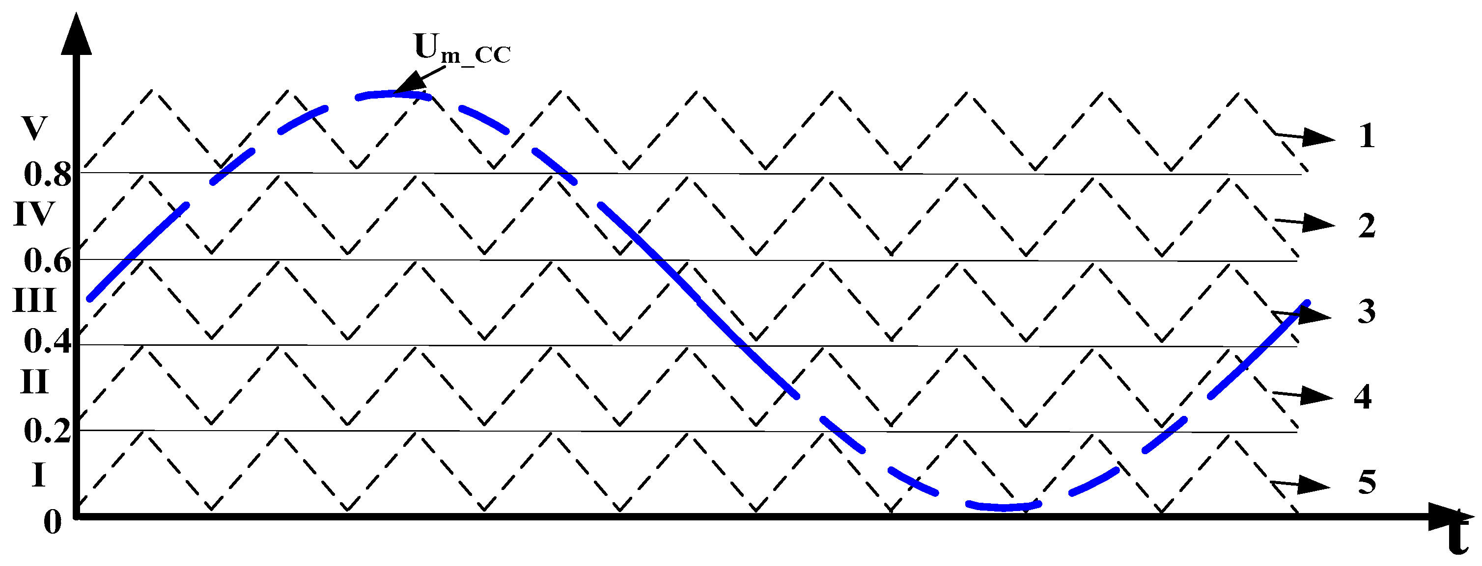
- In Area 1, when U m_CHB_1 > U m_CHB_2, the SM superposed with the bias value “0.4” has the longest forward access time to the main circuit, and the SMs superposed with the bias value “0” and “0.8” have the shortest forward access time to the main circuit.
- (2)
- In Area 2, when U m_CHB_1 < U m_CHB_2, the SM superposed with the bias 3 signal has the longest reverse access time to the main circuit, and the SM superposed with the bias 1 signal and the bias 5 signal has the shortest reverse access time to the main circuit.
4.2. Realization of Proposed Dynamic Carrier Bias Allocation Method for CHB
- (1)
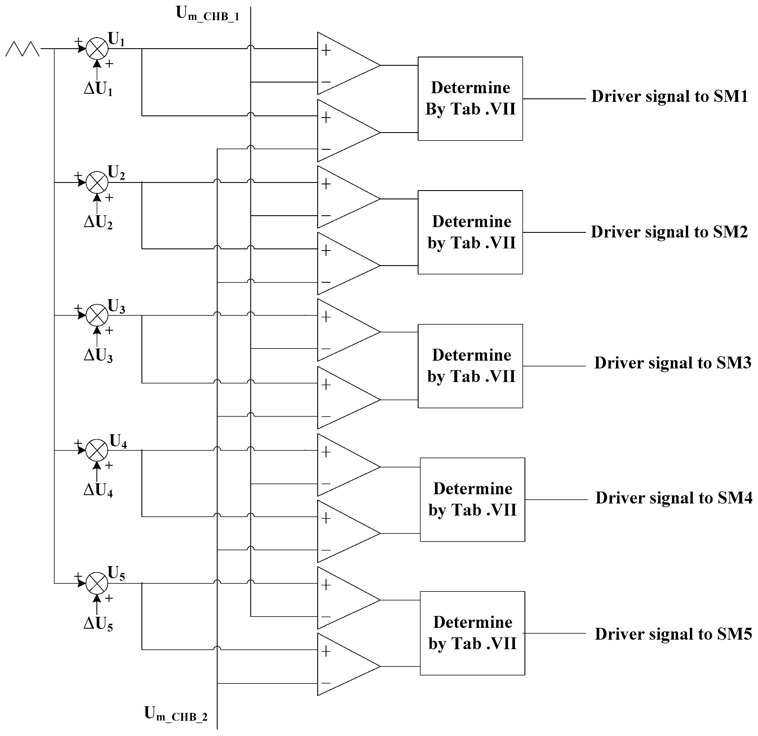
- The current real-time measured and the dual modulation signal generation method described in the Section 3.2 are used to determine the operation condition for the CHB structure at the current time (as defined in Equations (8) and (9)).
- (2)
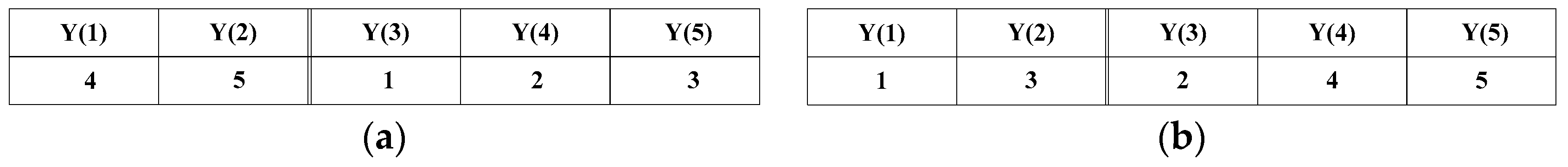
- The FPGA parallel calculation is used to select the maximum sub-module DC capacitor voltage and the minimum sub-module DC capacitor voltage at the current time. Uci (i = 1–N) are the DC capacitor voltages of the SMs, and they are compared to each other at the same time, which means that the time is limited. An array Y is used to record the comparative result. Y(1) would be equal to the SM index having the minimum DC capacitor voltage, Y(2) would be equal to the SM index having the maximum DC capacitor voltage. The other SMs indexes except the minimum and maximum DC capacitor voltages would also be assigned to the Y array by sequence after Y(2), it can be expressed as Equation (10):where IndexUc_min is the SM index having the minimum capacitor voltage, IndexUc_max is the SM index having the maximum DC voltage, for example, if in j triangular carrier signal wave cycle, SM4 has the lowest voltage and SM5 has the highest voltage, the Y array would be assigned like Figure 5a. And if in j + 1 triangular carrier signal wave cycle, SM1 has the lowest voltage and SM3 has the highest voltage, the Y array would be assigned like Figure 5b.
- (3)
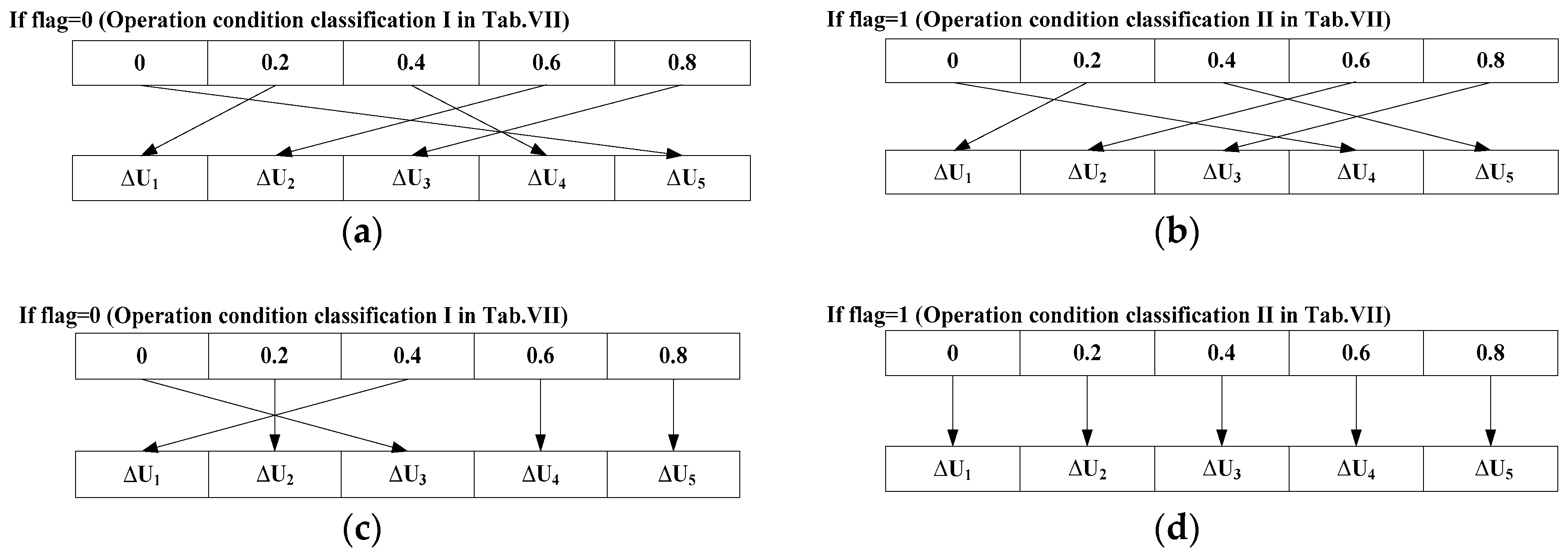
- Then, a new multiport triangular carrier signal bias selector array ΔU[Y(k)] has to be set up, as shown in Equations (11)–(13). Its index is Y(k). A flag is the symbol of operation condition classification of Table 7.
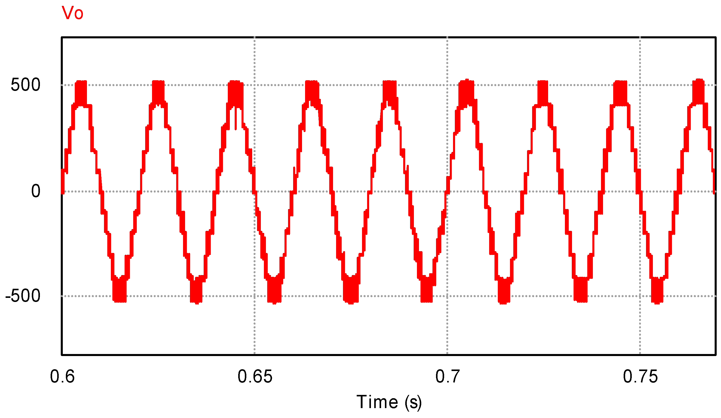
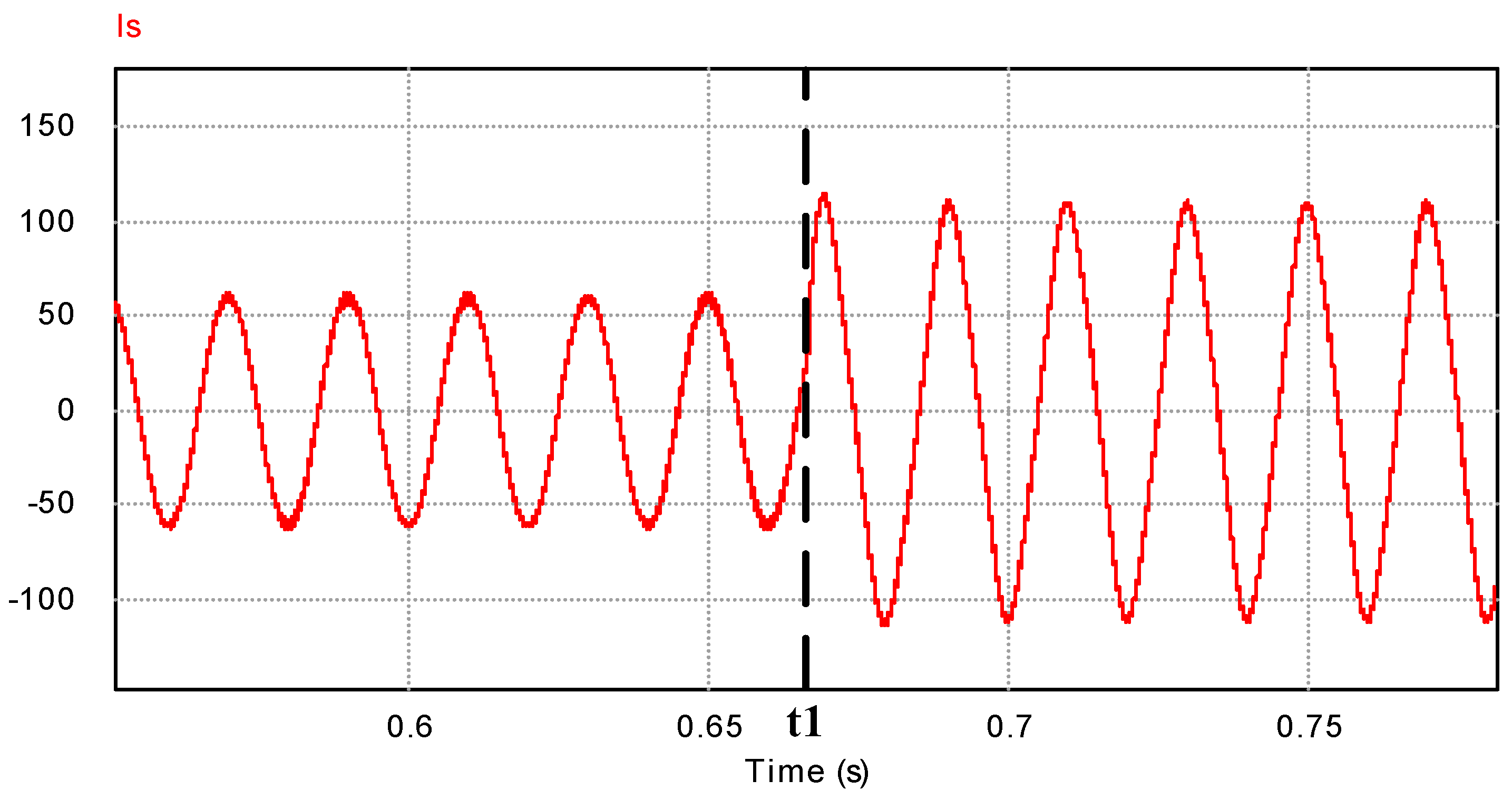
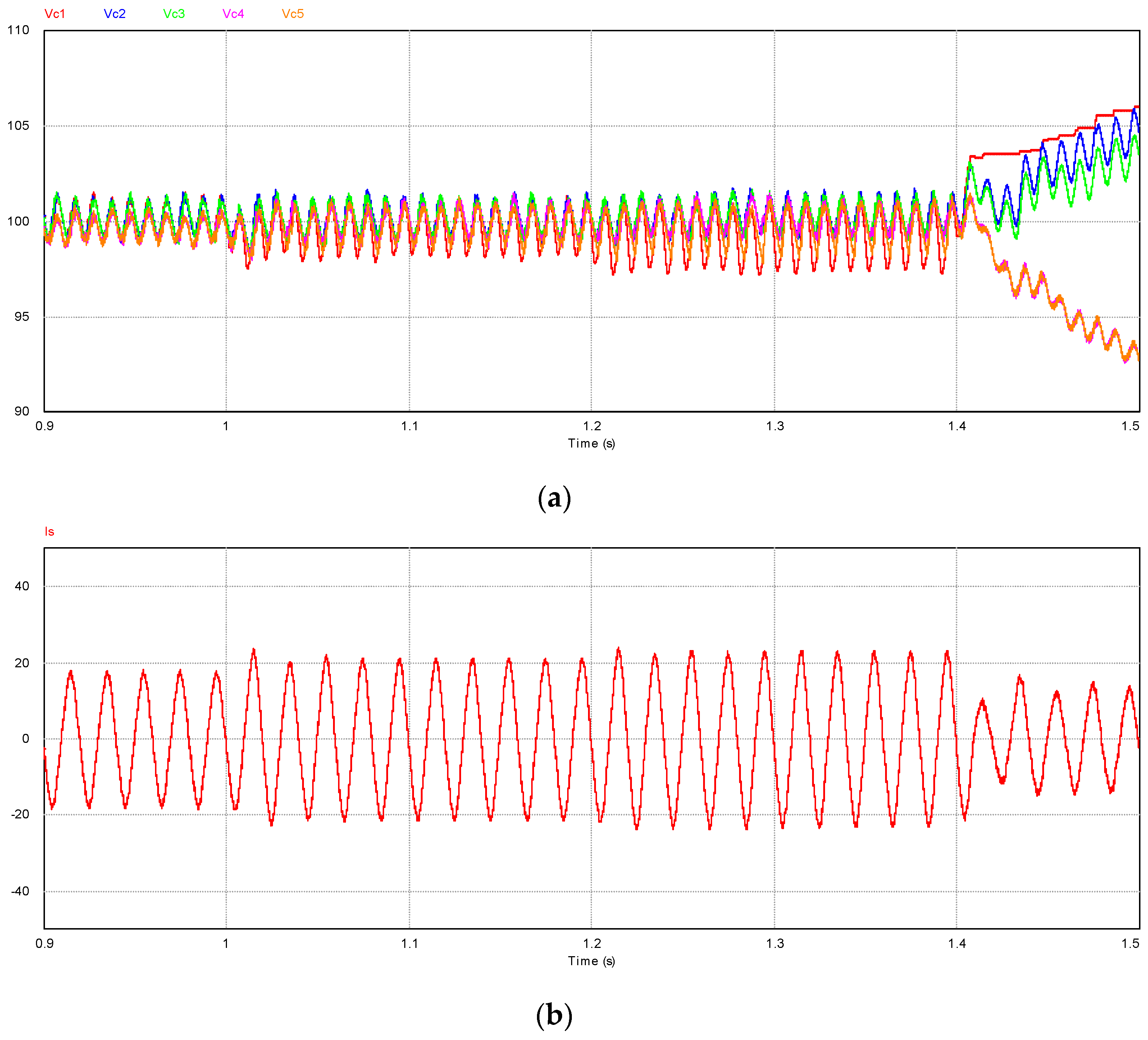
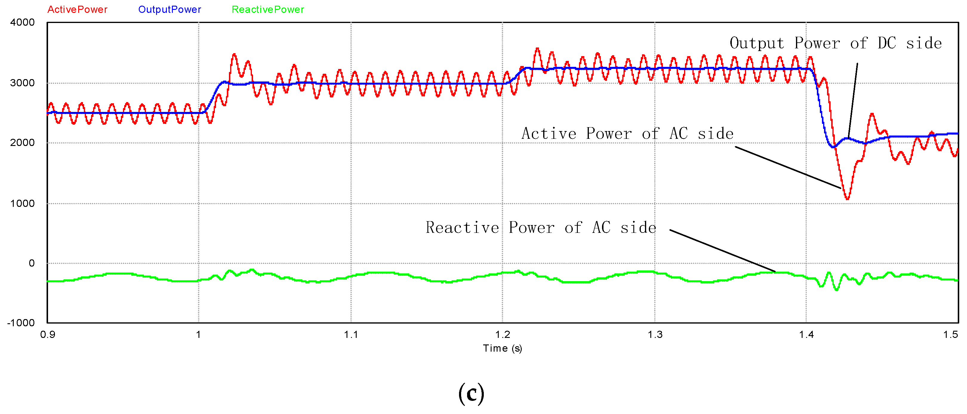
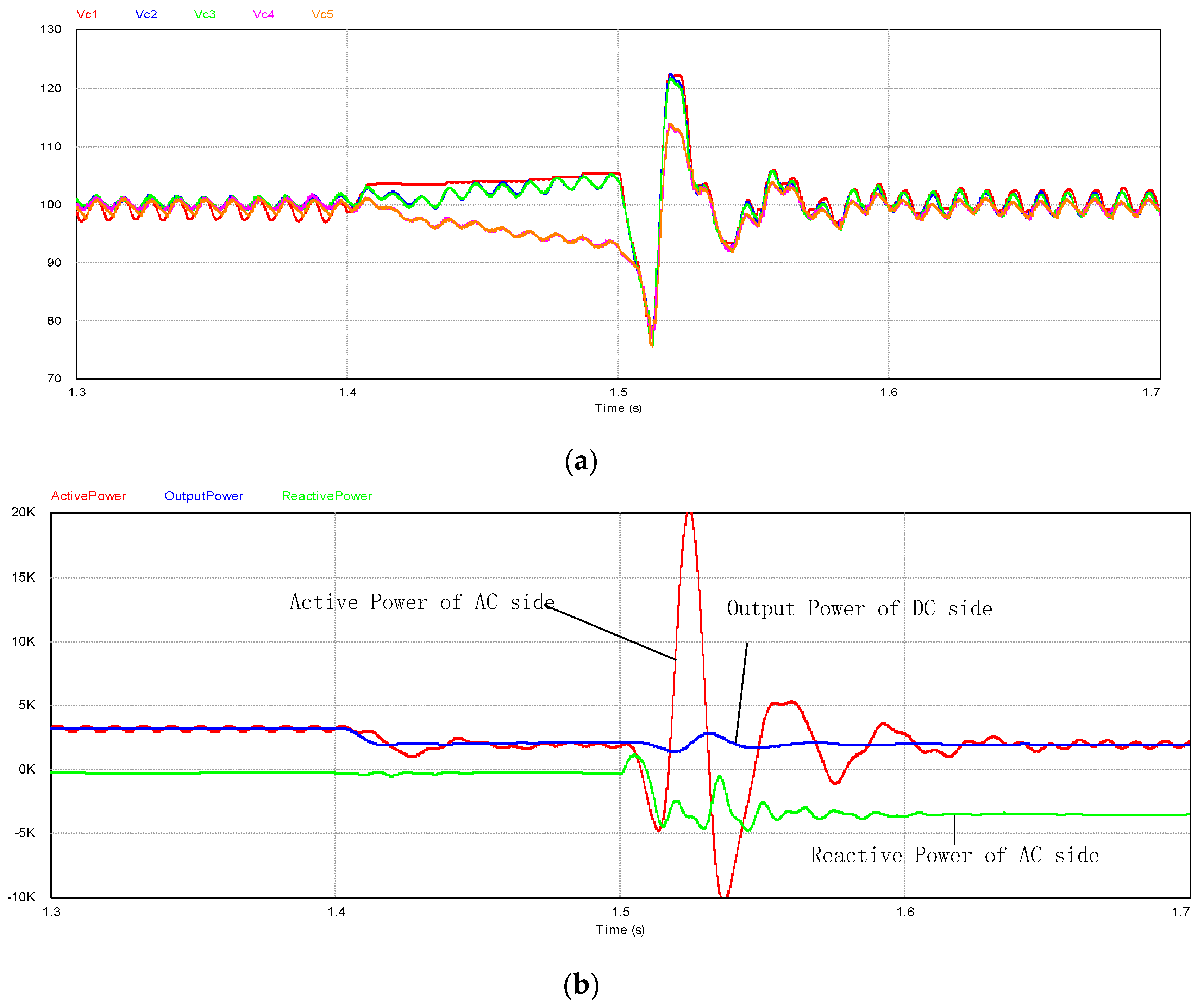
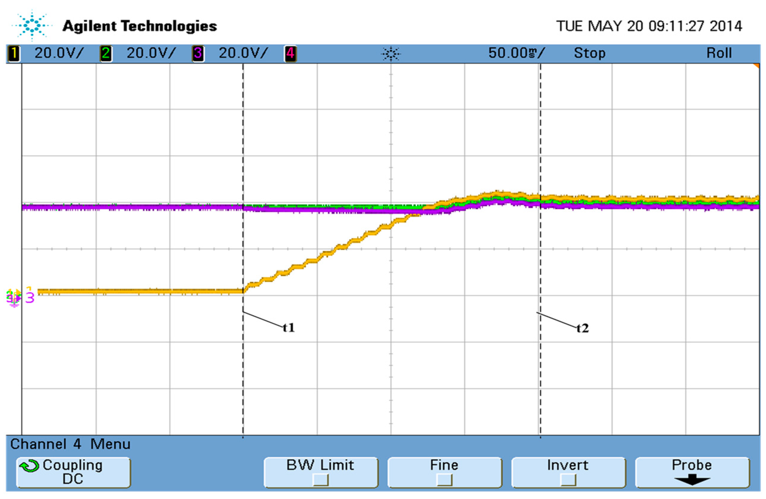
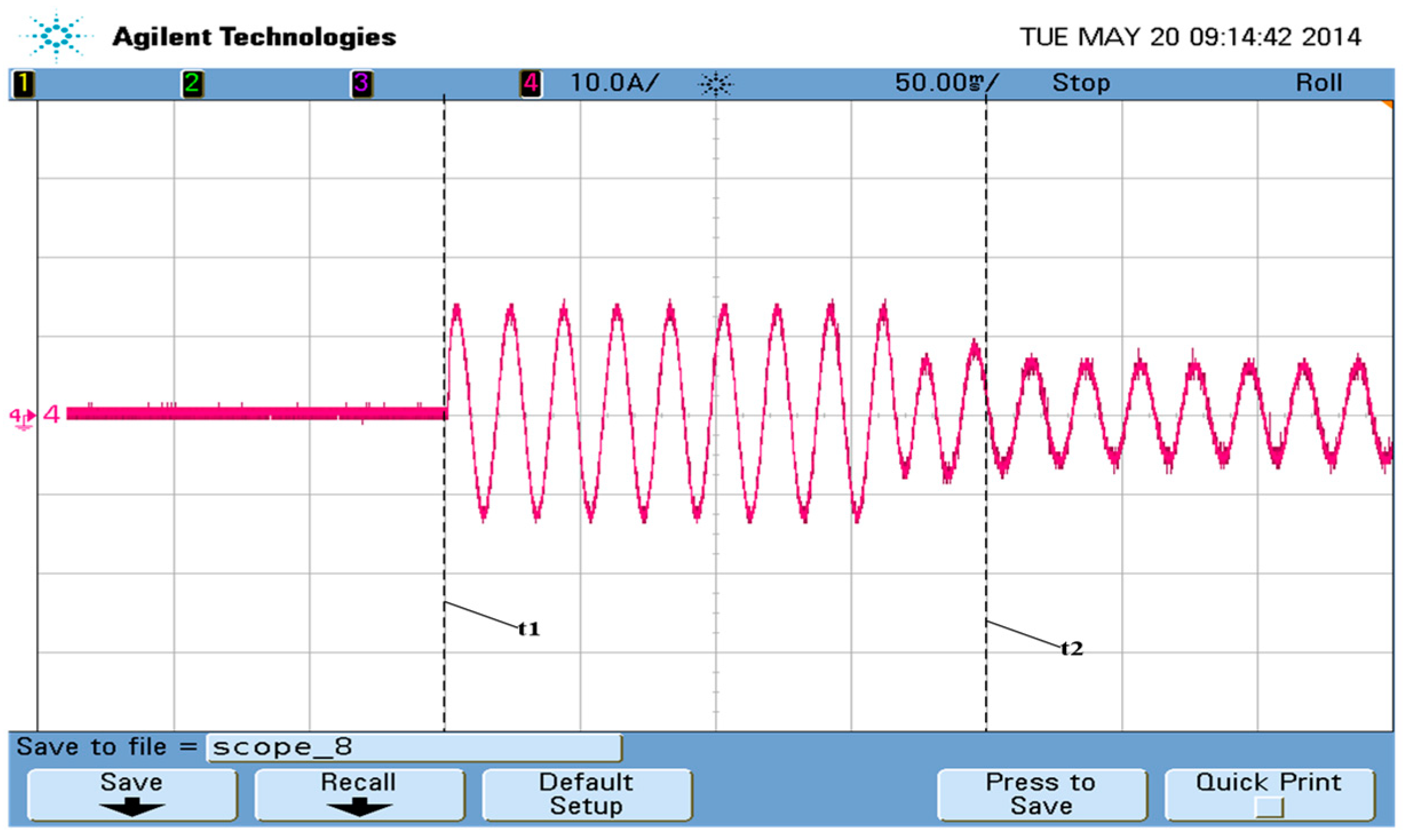
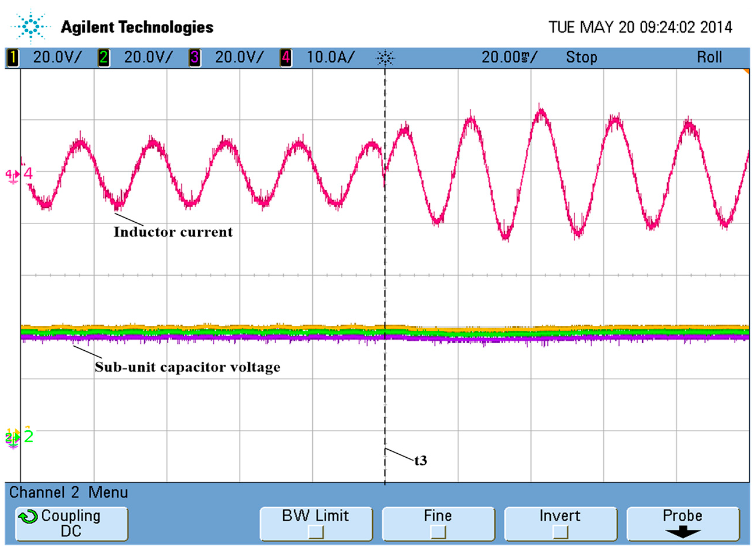
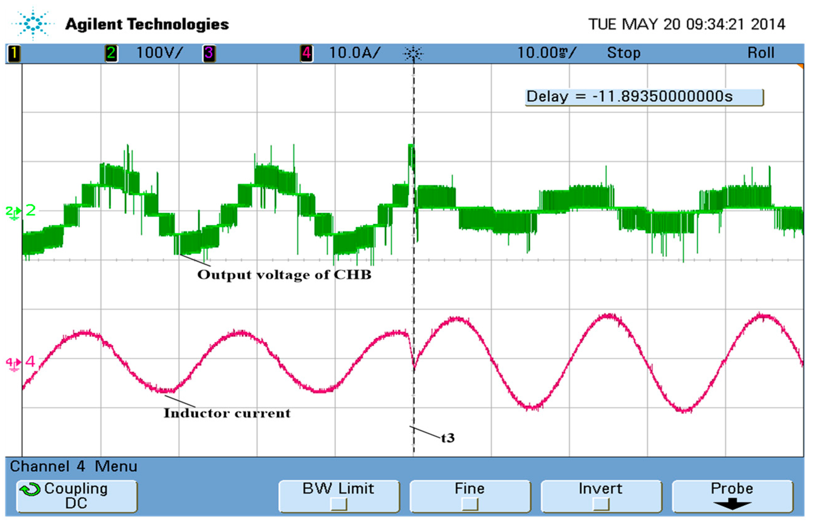
5. Simulation and Experiments
5.1. Simulation
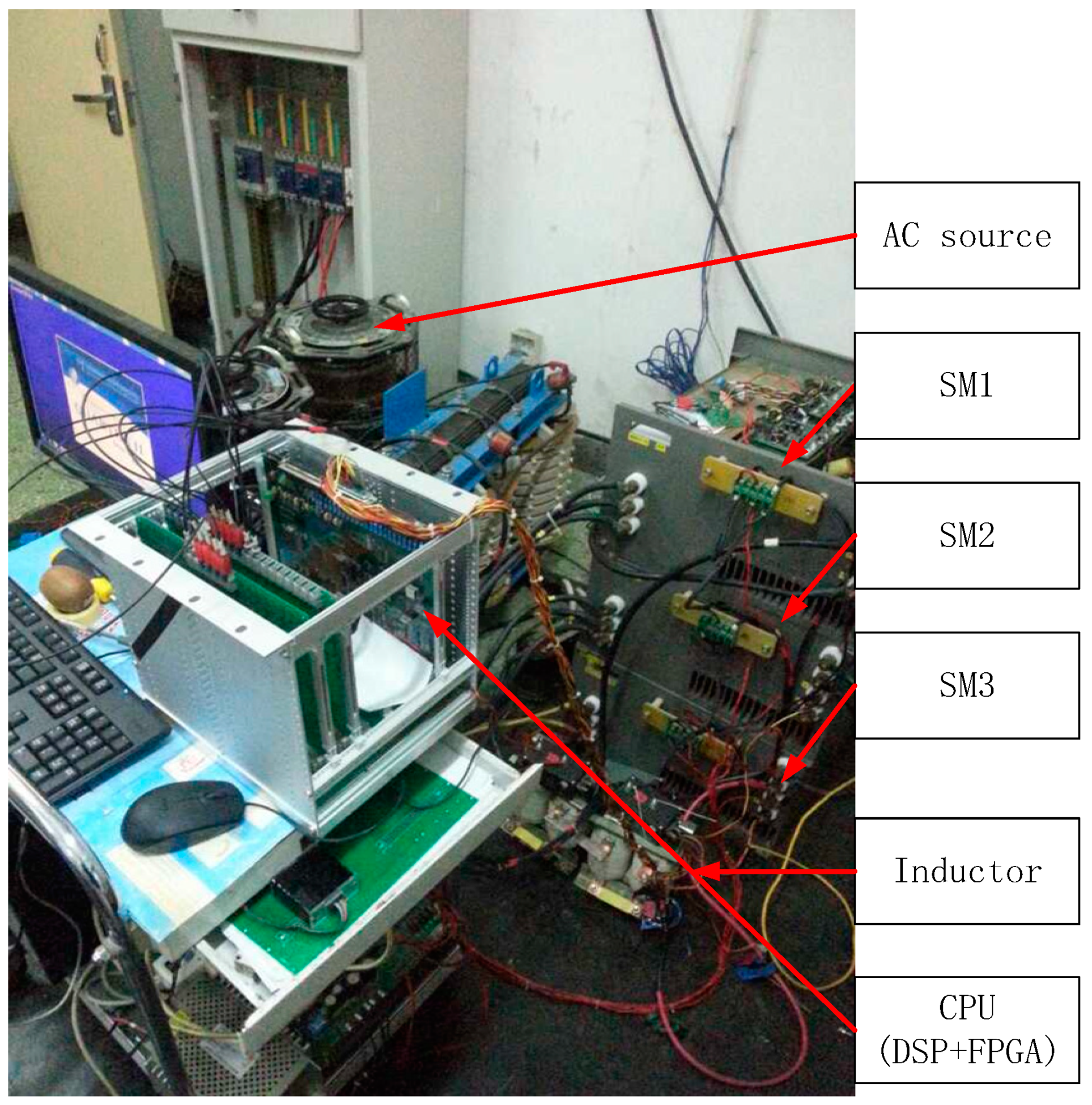
5.2. Experiments
6. Discussion
- Lower harmonic distortion in medium voltage application compared with NLM method, because of its AC side voltage is multilevel PWM waveform instead of step waveform;
- Less computational effort compared with predictive control method;
- Lower complexity of the control system compared with PS-PWM for no extra multiple proportional-integral control signal added to the reference voltage;
- Much stronger dynamic regulation ability under the conditions of asymmetric parameters of independent DC loads for it can quickly adjust the access time of each sub-module in the beginning of each sampling period such as NLM.
7. Conclusions
- (1)
- Simulation and experiment results show that this method has dynamic regulation ability to balance the DC voltage of each sub-module with asymmetry parameters of independent DC loads and a fast dynamic response for the entire system by allocate the bias of SMs flexibly;
- (2)
- Comparison analysis show that this method can reduce harmonic distortion in medium voltage applications compared with the NLM method when the number of sub-modules is insufficient for medium-voltage application while keep much stronger dynamic regulation ability because of the characteristics of the PWM method;
- (3)
- This method also facilitates engineering implementation in real applications because it has no issues of sorting (like the NLM method) and no need for extra multiple proportional-integral control signals added to the reference voltage (like the PD-PWM method), so the computational burden is also reduced.
Author Contributions
Funding
Conflicts of Interest
References
- Yang, Z.; Sun, J.; Li, S.; Huang, M.; Zha, X. An Adaptive Carrier Frequency Optimization Method for Harmonic Energy Unbalance Minimization in a Cascaded H-Bridge-Based Active Power Filter. IEEE Trans. Power Electron. 2018, 33, 1024–1037. [Google Scholar] [CrossRef]
- Wu, L.; Wu, M. Single-phase Cascaded H-bridge Multi- level Active Power Filter Based on Direct Current Control in AC Electric Railway Application. IET Power Electron. 2017, 10, 637–645. [Google Scholar] [CrossRef]
- Blahnik, V.; Kosan, T.; Peroutka, Z.; Talla, J. Control of a Single-phase Cascaded H-bridge Active Rectifier under Unbalanced Load. IEEE Trans. Power Electron. 2018, 33, 5519–5527. [Google Scholar] [CrossRef]
- Yang, D.; Yin, L.; Xu, S.; Wu, N. Power and Voltage Control for Single-Phase Cascaded H-Bridge Multilevel Converters under Unbalanced Loads. Energies 2018, 11, 2435. [Google Scholar] [CrossRef]
- Gautam, S.; Gupta, R. Switching Frequency Derivation for the Cascaded Multilevel Inverter Operating in Current Control Mode Using Multi band Hysteresis Modulation. IEEE Trans. Power Electron. 2014, 29, 1480–1489. [Google Scholar] [CrossRef]
- Rohner, S.; Bernet, S.; Hiller, R.; Sommer, R. Modulation, losses, and semiconductor requirements of modular multilevel converters. IEEE Trans. Ind. Electron. 2010, 57, 2633–2642. [Google Scholar] [CrossRef]
- Luo, C.; Luo, D.; Huang, S.; Wu, G.; Zhu, H.; He, Q. A Novel Control Strategy for DC-Link Voltage Balance and Reactive Power Equilibrium of a Single-Phase Cascaded H-Bridge Rectifier. Energies 2019, 12, 51. [Google Scholar] [CrossRef]
- Rezaei, M.; Iman-Eini, H.; Farhangi, S. Grid-connected Photovoltaic System based on a Cascaded H-Bridge Inverter. J. Power Electron. 2012, 12, 578–586. [Google Scholar] [CrossRef]
- Barrena, J.; Marroyo, L.; Vidal, M.; Apraiz, J. Individual Voltage Balancing Strategy for PWM Cascaded H-Bridge Converter-based STATCOM. IEEE Trans. Ind. Electron. 2008, 55, 21–29. [Google Scholar] [CrossRef]
- Du, S.; Liu, J. A Novel DC Voltage Control Method for STATCOM Based on Hybrid Multilevel H-Bridge Converter. IEEE Trans. Power Electron. 2013, 28, 101–110. [Google Scholar] [CrossRef]
- Holmes, D.; Lipo, T. Pulse Width Modulation for Power Converters Principles and Practice; Wiley-IEEE Press: New York, NY, USA, 2003; pp. 453–530. [Google Scholar]
- Chan, R.; Kwak, S. Improved Finite-Control-Set Model Predictive Control for Cascaded H-Bridge Inverters. Energies 2018, 11, 355. [Google Scholar] [CrossRef]
- Zhang, Y.; Wu, X.; Yuan, X.; Wang, Y.; Dai, P. Fast Model Predictive Control for Multilevel Cascaded H-bridge STATCOM with Polynomial Computation Time. IEEE Trans. Ind. Electron. 2016, 63, 5231–5243. [Google Scholar] [CrossRef]
- Zhang, Y.; Wu, X.; Yuan, X. A Simplified Branch and Bound Approach for Model Predictive Control of Multilevel Cascaded H-Bridge STATCOM. IEEE Trans. Ind. Electron. 2017, 64, 7634–7644. [Google Scholar] [CrossRef]
- Qi, C.; Chen, X.; Tu, P.; Wang, P. Cell-by-cell-based Finite-control-set Model Predictive Control for a Single-phase Cascaded H-bridge Rectifier. IEEE Trans. Power Electron. 2018, 33, 1654–1665. [Google Scholar] [CrossRef]
- Karamanakos, P.; Pavlou, K.; Manias, S. An Enumeration-Based Model Predictive Control Strategy for the Cascaded H-Bridge Multilevel Rectifier. IEEE Trans. Ind. Electron. 2014, 61, 3480–3489. [Google Scholar] [CrossRef]
- Townsend, C.D.; Summers, T.J.; Vodden, J.; Watson, A.J.; Betz, R.E.; Clare, J.C. Optimization of Switching Losses and Capacitor Voltage Ripple Using Model Predictive Control of a Cascaded H-bridge Multilevel Statcom. IEEE Trans. Power Electron. 2013, 28, 3077–3087. [Google Scholar] [CrossRef]
- Angulo, M.; Lezana, P. Level-shifted PWM for Cascaded Multilevel Converters with Even Power Distribution. In Proceedings of the 2007 IEEE Power Electronics Specialists Conference, Orlando, FL, USA, 17–21 June 2007; pp. 2373–2378. [Google Scholar]
- Ghazanfari, A.; Mokhtari, H. Simple Voltage Balancing Approach for CHB Multilevel Inverter Considering Low Harmonic Content Based on a Hybrid Optimal Modulation Strategy. IEEE Trans. Power Electron. 2012, 27, 2150–2158. [Google Scholar] [CrossRef]
- Mei, J.; Shen, K.; Xiao, B. A New Selective Loop Bias Mapping Phase Disposition PWM with Dynamic Voltage Balance Capability for Modular Multilevel Converter. IEEE Trans. Ind. Electron. 2014, 61, 798–807. [Google Scholar] [CrossRef]
- Mei, J.; Xiao, B.; Shen, K.; Tolbert, L.M.; Zheng, J.Y. Modular Multilevel Inverter with New Modulation Method and Its Application to Photovoltaic Grid-Connected Generator. IEEE Trans. Power Electron. 2013, 28, 5063–5073. [Google Scholar] [CrossRef]
- Davidson, C.C.; Trainer, D.R. Innovative concepts for hybrid multi-level converters for HVDC power transmission. In Proceedings of the 9th IET International Conference an AC and DC Power Transmission, London, UK, 19–21 October 2010; pp. 1–5. [Google Scholar]
- Cross, A.M.; Trainer, D.R.; Crookes, R.W. Chain-link based HVDC Voltage Source Converter using current injection. In Proceedings of the 9th IET International Conference an AC and DC Power Transmission, London, UK, 19–21 October 2010; pp. 1–5. [Google Scholar]
- Zhu, J.; Wei, T.; Huo, Q.; Yin, J. A Full-bridge Director Switches based Multilevel Converter with DC Fault Blocking Capability and Its Predictive Control Strategy. Energies 2019, 12, 91. [Google Scholar] [CrossRef]


| Mode | S1 | S2 | USMi | IL | The State of the Sub-Module | The State of the DC-Link Capacitor |
|---|---|---|---|---|---|---|
| 1 | 1 | 0 | Uci | >0 | ON | Charging |
| 2 | 1 | 0 | Uci | <0 | ON | Discharging |
| 3 | 0 | 1 | 0 | >0 | OFF | Uncharged |
| 4 | 0 | 1 | 0 | <0 | OFF | Uncharged |
| Mode | S1 | S2 | S3 | S4 | USMi | IL | The State of the DC-Link Capacitor |
|---|---|---|---|---|---|---|---|
| 1 | 1 | 0 | 0 | 1 | Uci | >0 | Charging |
| 2 | 1 | 0 | 0 | 1 | Uci | <0 | Discharging |
| 3 | 0 | 1 | 1 | 0 | −Uci | >0 | Discharging |
| 4 | 0 | 1 | 1 | 0 | −Uci | <0 | Charging |
| 5 | 1 | 1 | 0 | 0 | 0 | >0 | Uncharged |
| 6 | 0 | 0 | 1 | 1 | 0 | <0 | Uncharged |
| Relationship of Modulation Signal (Um_CC) and Corresponding Triangular Carrier Signal (Utsi) | USMi | IL | State of Capacitor |
|---|---|---|---|
| Um_CC > Utsi | Uci | >0 | Charging |
| Um_CC > Utsi | Uci | <0 | Discharging |
| Um_CC < Utsi | 0 | >0 | Uncharged |
| Um_CC < Utsi | 0 | <0 | UnCharged |
| Vertical Region No. of Um_CC | Sub-Module Switch Signals with Different Triangular Carrier Signals Bias Value in Figure 2 | ||||
|---|---|---|---|---|---|
| SM 1 | SM 2 | SM 3 | SM 4 | SM 5 | |
| I | P1 | 0 | 0 | 0 | 0 |
| II | 1 | P2 | 0 | 0 | 0 |
| III | 1 | 1 | P3 | 0 | 0 |
| IV | 1 | 1 | 1 | P4 | 0 |
| V | 1 | 1 | 1 | 1 | P5 |
| Relationship of Modulation Signal (Um_CHB) and Corresponding Triangular Carrier Signal (Utsi) | USMi | IL | State of Capacitor |
|---|---|---|---|
| Um_CHB1 > Utsi > Um_CHB2 | Uci | >0 | Charging |
| Um_CHB1 > Utsi > Um_CHB2 | Uci | <0 | Discharging |
| Utsi> Um_CHB1, Utsi > Um_CHB2 | 0 | >0 | Uncharged |
| Utsi< Um_CHB1, Utsi < Um_CHB2 | 0 | <0 | Uncharged |
| Um_CHB1< Utsi < Um_CHB2 | −Uci | >0 | Discharging |
| Um_CHB1< Utsi < Um_CHB2 | −Uci | <0 | Charging |
| Relationship of Um_CHB1 and Um_CHB2 | Vertical Region No. of Um_CHB1 | Sub-Module Switch Signals with Different Triangular Carrier Signals Bias Value in Figure 3 | ||||
|---|---|---|---|---|---|---|
| SM1 | SM 2 | SM 3 | SM 4 | SM 5 | ||
| Um_CHB1 < Um_CHB2 (Area II) | I | −P1 | −1 | −1 | −1 | −P5 |
| II | 0 | −P2 | −1 | −P4 | 0 | |
| III | 0 | 0 | −P3 | 0 | 0 | |
| Um_CHB1 > Um_CHB2 (Area I) | III | 0 | 0 | P3 | 0 | 0 |
| IV | 0 | P2 | 1 | P4 | 0 | |
| V | P1 | 1 | 1 | 1 | P5 | |
| Operation Condition Classification | Condition | ||
|---|---|---|---|
| Area Partition in Figure 3 | Current Direction | ||
| I (Flag = 0) | Area 1 | IL > 0 | SM superposed with bias value “0.4” (SM for triangular carrier signal in vertical coordinate III area) is in fastest charging state; SM superposed with bias “0” and bias “0.8” (SM for triangular carrier signal in vertical coordinate I area and V area) is in slowest charging state. |
| Area 2 | IL < 0 | ||
| II (Flag = 1) | Area 1 | IL < 0 | SM superposed with value “0.4” (SM for triangular carrier signal in vertical coordinate III area) is in fastest discharging state; SM superposed with bias “0” and bias “0.8” (triangular carrier signal in vertical coordinate I area and V area) is in slowest discharging state. |
| Area 2 | IL > 0 | ||
| Parameter Name | Parameter Value |
|---|---|
| Sub-unit capacitor voltage rating | 100 V |
| Sub-unit number N | 5 |
| Sub-unit capacitor value C | 5 mF |
| Grid-connection inductor L | 10 mH |
| AC voltage frequency f | 50 Hz |
| Carrier frequency | 2000 Hz |
| Parameter Name | Parameter Value |
|---|---|
| Sub-unit capacitor voltage rating | 40 V |
| Sub-unit number N | 3 |
| Sub-unit capacitor value C | 5 mF |
| Grid-connection inductor L | 6 mH |
| AC voltage frequency f | 50 Hz |
| Carrier frequency | 2000 Hz |
| Harmonic Distortion in MV Application | Harmonic Distortion in HV Application | Amount of Computation | The Complexity of the Control System | Dynamic Regulation Ability with Asymmetric Parameters of Independent DC Loads | |
|---|---|---|---|---|---|
| Proposed PD-PWM | +++ | +++ | ++ | +++ | +++ |
| The LBM PD-PWM | +++ | +++ | +++ | +++ | + |
| Conventional PD-PWM | +++ | +++ | +++ | +++ | + |
| PS-PWM | +++ | +++ | ++ | ++ | ++ |
| NLM | + | +++ | + | ++ | +++ |
| Predictive control | +++ | +++ | + | + | +++ |
© 2019 by the authors. Licensee MDPI, Basel, Switzerland. This article is an open access article distributed under the terms and conditions of the Creative Commons Attribution (CC BY) license (http://creativecommons.org/licenses/by/4.0/).
Share and Cite
Zhu, J.; Wei, T.; Ma, M.; Han, L. Simple DC-Link Voltage Balancing Approach for Cascaded H-Bridge Rectifier with Asymmetric Parameters of Independent DC Loads. Energies 2019, 12, 1654. https://doi.org/10.3390/en12091654
Zhu J, Wei T, Ma M, Han L. Simple DC-Link Voltage Balancing Approach for Cascaded H-Bridge Rectifier with Asymmetric Parameters of Independent DC Loads. Energies. 2019; 12(9):1654. https://doi.org/10.3390/en12091654
Chicago/Turabian StyleZhu, Jin, Tongzhen Wei, Ming Ma, and Libo Han. 2019. "Simple DC-Link Voltage Balancing Approach for Cascaded H-Bridge Rectifier with Asymmetric Parameters of Independent DC Loads" Energies 12, no. 9: 1654. https://doi.org/10.3390/en12091654