Abstract
This paper presents a highly efficient three-port converter to integrate energy storage (ES) and wireless power transfer (WPT) systems. The proposed converter consists of a bidirectional DC-DC converter and an AC-DC converter with a resonant capacitor. By sharing an inductor and four switches in the bidirectional DC-DC converter, the bidirectional DC-DC converter operates as a DC-DC converter for ES systems and simultaneously as a DC-AC converter for WPT systems. Here, four switches are turned on under the zero voltage switching conditions. The AC-DC converter for WPT system achieves high voltage gain by using a resonance between the resonant capacitor and the leakage inductance of a receiving coil. A 100-W prototype was built and tested to verify the effectiveness of the converter; it had a maximum power-conversion efficiency of 95.9% for the battery load and of 93.8% for the wireless charging load.
1. Introduction
Photovoltaics (PVs) constitute a promising alternative energy source due to diverse applications and the ubiquity of sunlight [1,2,3,4]. Residential PV systems consist of a PV module and a PV inverter, and it converts sunlight into electricity. However, energy output by PV systems is not constant because it is affected by weather conditions and the day/night cycle. Therefore, energy storage (ES) systems are used to efficiently manage the PV energy. They consist of a battery and a bidirectional DC-DC converter that connects to the PV system [5,6,7]. Besides, in the near future, the wireless power transfer (WPT) systems will be widely used to wirelessly charge laptops as well as cell phones in many households [8,9,10,11]. Therefore, future PV energy delivery and management infrastructure for residential applications will consist of PV systems, ES systems, and WPT systems (Figure 1a).
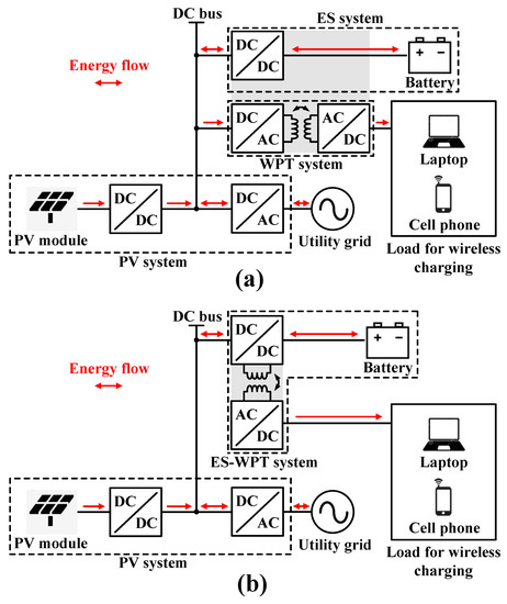
Figure 1.
Future photovoltaic (PV) energy delivery and management infrastructure; (a) typical topology, (b) proposed topology.
Three-port converters have been used to reduce the cost and size of infrastructure, such as micro-grids and smart grids [12,13,14,15,16,17,18]. The infrastructure consists of several systems, so its cost and size increase in proportion to the number of systems. To alleviate this problem, two systems are integrated through on a three-port converter. The three-port converters usually add a port to a typical converter that has two ports, either by using a three-winding transformer instead of a two-winding transformer [13,14,15] or by using the storage capacitor in the typical converter as a third port [16,17,18].
Many three-port converters have been introduced to integrate renewable energy sources (e.g., PV, fuel cell, wind turbine) with ES systems, but a three-port converter to integrate ES and WPT systems has not been considered. Therefore, this paper presents a three-port converter that can integrate the ES and WPT systems that will be used in future PV energy delivery and management infrastructure for residential applications (Figure 1b). The proposed three-port converter consists of a bidirectional DC-DC converter for an ES system and an AC-DC converter with a resonant capacitor. The bidirectional DC-DC converter can also operate as a DC-AC converter of the WPT system because the inductor in the bidirectional DC-DC converter is also used as a transmitting coil for a WPT system. With these few components, the proposed converter can store energy for the ES system and simultaneously transfer the energy by using a WPT system. The proposed converter has a high power-conversion efficiency by achieving zero voltage switching (ZVS) turn-on for switches, and has high voltage gain for WPT by using a resonance between a resonant capacitor and a leakage inductance of a receiving coil.
2. Proposed Three-Port Converter
2.1. Circuit Structure
The proposed converter (Figure 2a) combines the structures of a bidirectional DC-DC converter and an AC-DC converter.
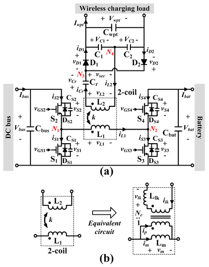
Figure 2.
(a) Circuit structure of the proposed converter. (b) Equivalent circuit of the two-coil structure.
The bidirectional DC-DC converter is located between a DC bus and a battery to transfer the energy in both directions (DC bus ↔ battery). This converter consists of four switches (S1, S2, S3, S4), two filter capacitors (bus capacitor, Cbus, with capacitance, Cbus, and battery capacitor, Cbat, with capacitance, Cbat), and an inductor (L1 with inductance L1). In addition, it can transfer the energy of the DC bus (or battery) to the wireless charging load because L1 also acts as a transmitting coil for WPT.
The AC-DC converter is connected to a wireless charging load, such as a cell phone or laptop, and it has a receiving coil (L2 with inductance L2) for WPT, a filter capacitor (WPT capacitor, Cwpt, with capacitance, Cwpt), a resonant capacitor (Cr with capacitance, Cr), and a voltage doubler rectifier that consists of two diodes (D1, D2) and two doubler capacitors (C1 with capacitance, C1, and C2 with capacitance, C2).
L1 and L2 are parts of the two-coil structure; they are coupled magnetically with a coupling coefficient, k, to transfer the energy wirelessly. Based on [19,20], the two-coil structure can be represented as a transformer with a leakage inductor (Llk with inductance, Llk), an effective turn ratio (Ne), and a magnetizing inductor (Lm with inductance, Lm), where , , and (Figure 2b).
Four switches achieve the ZVS turn-on by using the stored energy in L1. Llk resonates with Cr, and high voltage gain between the DC bus and wireless charging load is achieved by setting the switching frequency, fS, to the resonant frequency, fr, between Llk and Cr. The voltage doubler rectifier converts AC voltage to DC voltage for wireless charging load, and clamps the reverse voltages of D1 and D2 to WPT voltage, Vwpt.
2.2. Principle of Operation
The proposed converter operates at a fixed switching frequency (fS = 1/TS), where TS is a switching period, and it controls the voltage gain between the DC bus voltage, Vbus, and battery voltage, Vbat, by changing the duty ratios of S1, S2, S3, and S4; the duty ratios of S2 and S3 are defined as D, and the duty ratios of S1 and S4 are defined as 1–D. In addition, the voltage gain between Vbus and Vwpt is adjusted by using Ne.
The equivalent circuits (Figure 3) and operating waveforms (Figure 4) were obtained under the following assumptions and conditions: (1) All components are lossless, (2) C1, C2, Cbus, Cbat, and Cwpt are large enough to assume that VC1, VC2, Vbus, Vbat, and Vwpt are constant voltage sources, (3) fr = fS, and (4) the converter operates in a steady state. The converter operates in four modes.
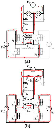
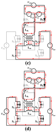
Figure 3.
(a) Circuit diagrams for the operation in Mode 1. (b) Circuit diagrams for the operation in Mode 2. (c) Circuit diagrams for the operation in Mode 3. (d) Circuit diagrams for the operation in Mode 4.
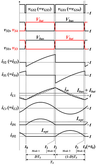
Figure 4.
Operational waveforms of the proposed converter.
Mode 1 (Figure 3a, t0 ≤ t ≤ t1): This mode starts at t = t0 when S2 and S3 are turned on. At this time, S2 and S3 achieve ZVS turn-on because the body diodes, DS2 and DS3, of S2 and S3 are turned on before t = t0. During this mode, the voltage, vm, of Lm becomes Vbus, and the current, im, of Lm is:
where . Cr has voltage vCr = NeVbus − VC1–vlk and current iCr = ilk, and iCr(t0) = 0. Therefore:
where and . The current, iD1, of D1 is equal to iCr for t0 ≤ t ≤ t1.
Mode 2 (Figure 3b, t1 ≤ t ≤ t2): At t = t1, S2 and S3 are turned off, and S1 and S4 remain in the off-states to prevent a shoot-through problem. This mode is known as dead time. During this mode, the output capacitance, CS1, of S1 discharges from Vbus to 0, and the output capacitance, CS2, of S2 charges from 0 to Vbus. In addition, the output capacitance, CS4, of S4 discharges from Vbat to 0, and the output capacitance, CS3, of S3 charges from 0 to Vbat. Shortly after the discharging and charging processes are finished, the body diodes, DS1 and DS4, of S1 and S4 are turned on.
Mode 3 (Figure 3c, t2 ≤ t ≤ t3): At t = t2, S1 and S4 are turned on under ZVS conditions because the body diodes, DS1 and DS4, are turned on before t = t2. During this mode:
because vm = −Vbat. iCr is obtained using vCr = − NeVbat + VC2 − vlk and iCr(t2) = 0 as:
where . At t = t2, D2 is turned on, and the current, iD2, of D2 is −iCr.
Mode 4 (Figure 3d, t3 ≤ t ≤ t4): S2 and S3 remain in the off-states because this mode is the dead time interval. During this mode, CS2 discharges from Vbus to 0, and CS1 charges from 0 to Vbus. In addition, CS3 discharges from Vbat to 0, and CS4 charges from 0 to Vbat. Shortly after the discharging and charging processes are finished, DS2 and DS3 are turned on.
2.3. Voltage Gain
The proposed converter has one input port (DC bus) and two output ports (battery and wireless charging load). Therefore, it has (Equation (1)) a voltage gain, Gbb, between the DC bus and battery and (Equation (2)) a voltage gain, Gwb, between the DC bus and wireless charging load.
(1) Gbb = Vbat/Vbus
For one TS, the average voltages of Cbus and Cbat are Vbus and Vbat, respectively. Then, the average voltage at node N1 between S1 and S2 is DVbus, and the average voltage at node N2 between S3 and S4 is given by (1-D) Vbat. The average voltage of L1 is zero due to the volt-second balance law for the inductor, and the average currents of switches are given by <iS2> = <iS3> = Ibus and <iS1> = <iS4> = −Ibat because the average current of the capacitor is zero by the charge balance law. Therefore, the average model of the circuit can be obtained (Figure 5). In this average model, the series resistance, RS, is the sum of RL1 and 2Ron, where RL1 and Ron are a winding resistance of L1 and on-resistance of a switch, respectively.
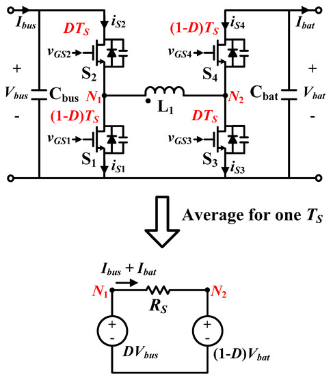
Figure 5.
Average model between node N1 and node N2.
By applying Kirchhoff’s voltage law (KVL) to the closed-loop that contains DVbus, RS, and (1-D) Vbat, the voltage gain Gbb ( = Vbat/Vbus) is obtained as:
where . In most cases, , so:
(2) Gwb = Vwpt/Vbus
Based on the four nodes (N1, N2, N3, and N4) in Figure 2a, the circuit of the proposed converter can be simplified (Figure 6a). Here, the square voltage, vac, between N1 and N2 is Vbus − (Ibus + Ibat)RS for DTS and − Vbat − (Ibus + Ibat)RS for (1-D)TS. Then, the current iac is iL1 − (Ibus + Ibat), and the square voltage, vac2, between N3 and N4 becomes Vwpt/2 for 0.5TS and −Vwpt/2 for the other 0.5TS. The current iac2 is given by iCr.
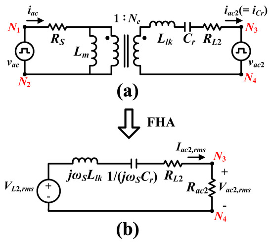
Figure 6.
(a) Equivalent circuit based on four nodes (N1, N2, N3, and N4). (b) AC model in the secondary winding side after applying fundamental harmonic approximation (FHA).
By applying fundamental harmonic approximation (FHA) to vac, iac, iac2, and vac2, the following root mean square (RMS) values are obtained (Figure 6b); VL2,rms is the RMS value of the first harmonic component in the voltage, vL2, of L2, and it is given by:
where:
and:
are RMS values of the first harmonic components in iac2 and vac2, respectively. Then, the equivalent resistance, Rac2, between N3 and N4 is obtained using Equations (8) and (9) as:
where . By applying KVL to the closed-loop in Figure 6b, the relation between VL2,rms and Vac2,rms is given by:
where RL2 is a winding resistance of L2. Then, substituting Equations (7) and (9) into Equation (11) yields:
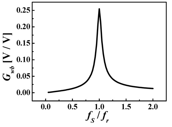
Figure 7.
Voltage gain (Gwb) between Vbus and Vwpt according to fS.
Therefore, Cr should be chosen to obtain the maximum voltage gain (Gwb) between Vbus and Vwpt. Because and , Cr can be determined as:
2.4. Magnetic Saturation
The coil structure, which consists of a transmitting coil (L1) and a receiving coil (L2), can use magnetic bars to increase efficiency and reduce magnetic fields that can interfere with nearby electronics [21,22,23]. Based on [24,25], the magnetic flux density (BC) of the coil structure is given by:
where µ0 is a vacuum permeability, is an effective relative permeability, N is the number of turns, im,peak is a peak value of im, lm is the mean magnetic path length, µr is a relative permeability, and lg is thee air-gap length.
Because the proposed converter has a DC bias current (=Ibus + Ibat) of L1, im,peak is given by:
Magnetic saturation can be caused by this DC bias current because the DC bias current increases BC by increasing im,peak. There are two methods to solve the problem of the DC bias current [26,27]. First, decreasing N reduces BC. Second, increasing lg reduces BC by decreasing µe. However, lg is determined by a distance, ld, between L1 and L2. Therefore, the following condition for preventing magnetic saturation can be obtained using BC < Bsat, (Equations (14) and (15)) as:
where Bsat is a saturation flux density of magnetic material.
3. Experimental Results
A prototype (Figure 8) of the proposed converter was fabricated using selected components and circuit parameters (Table 1), then tested to verify the operation of the proposed converter.
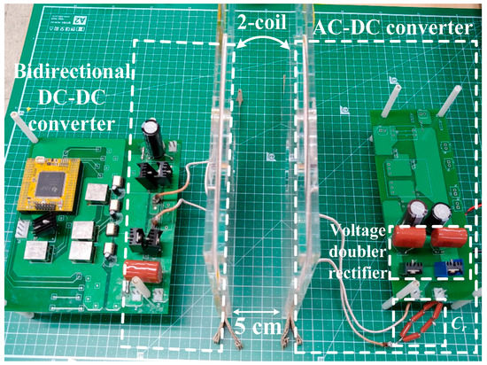
Figure 8.
Photograph of the prototype.

Table 1.
Values of the components used for the prototype.
The voltage and current waveforms of S1 and S2 were measured at Vbus = 400 V, Vbat = 400 V, fS = 400 kHz, and Pwpt (or Pbat) = 20 and 100 W (Figure 9). At both Pwpt = 20 W (Figure 9a) and Pwpt = 100 W (Figure 9b), the voltage stresses of S1 and S2 were measured as 400 V, which is equal to Vbus, and S1 and S2 achieved ZVS turn-on. In addition, S3 and S4 achieved ZVS turn-on at these conditions because iS1 = iS4 and iS2 = iS3. Even at both Pbat = 20 W (Figure 9c) and Pbat = 100 W (Figure 9d), all switches were turned on under the ZVS condition, which improves the power-conversion efficiency, ηe.
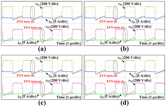
Figure 9.
Voltage and current waveforms of switches (S1, S2) measured at Pwpt = (a) 20 W and (b) 100 W or at Pbat = (c) 20 and (d) 100 W.
The theoretical Vwpt obtained from Equation (13) was compared with the experimental Vwpt measured at Vbus = 400 V, Vbat = 400 V, and Pwpt = 20 W~100 W (Figure 10). The theoretical Vwpt was higher than experimental Vwpt at all Pwpt, but the difference was <3%. This result shows that Equation (13) predicts the experimental Vwpt with little error. In addition, Vwpt was almost constant regardless of Pwpt.
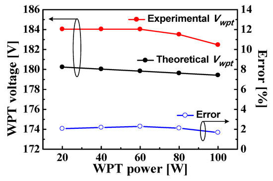
Figure 10.
Comparison between experimental Vwpt and theoretical Vwpt.
The power-conversion efficiencies (ηe,wpt for the wireless charging load and ηe,bat for the battery load) were measured at Vbus = 400 V, Vbat = 400 V, fS = 400 kHz, and Pwpt (or Pbat) = 20 W~100 W (Figure 11). The proposed converter had the highest ηe,wpt = 93.8% at Pwpt = 100 W (Figure 11a) and had the highest ηe,bat = 95.9% at Pbat = 100 W (Figure 11b). At low Pwpt = 20 W, the measured ηe,wpt was 82.5% (Figure 11a), and the measured ηe,bat was 83.5% at low Pbat = 20 W (Figure 11b). In addition, the measured ηe,bat was higher than the measured ηe,wpt because the wireless power loss during transfer between two coils is included in ηe,wpt. These results show that the proposed converter had high ηe,wpt > 82% and high ηe,bat > 83% for all operating ranges due to the ZVS turn-on of all switches.
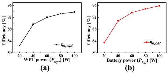
Figure 11.
(a) Power-conversion efficiency, ηe,wpt, measured at Pwpt = 20 W~100 W. (b) Power-conversion efficiency, ηe,bat, measured at Pbat = 20 W~100 W.
The transient response of Vwpt was measured at Vbus = 400 V, Vbat = 400 V, and fS = 400 kHz, while changing the wireless charging load from 20% to 100% and from 100% to 20% (Figure 12). At the load transition, the maximum voltage spike of Vwpt was measured as 14 Vp.p, and Vwpt returned to the steady-state within 81 ms.
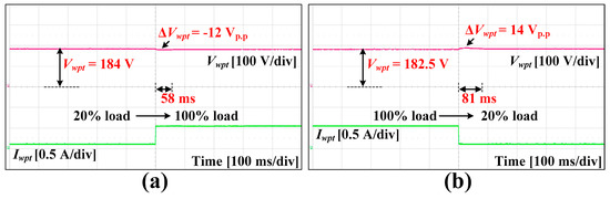
Figure 12.
Transient responses of Vwpt while changing the wireless charging load (a) from 20% to 100% and (b) from 100% to 20%.
In addition, the transient response of Vbat was measured while changing the battery load from 20% to 100% and from 100% to 20% under the same conditions as in Figure 12 (Figure 13). The maximum voltage spike of Vbat was measured as 61 Vp.p when the load changed, and Vbat returned to the steady state within 125 ms. These experiment results of the transient response show that the proposed converter can operate properly despite sudden load changes.
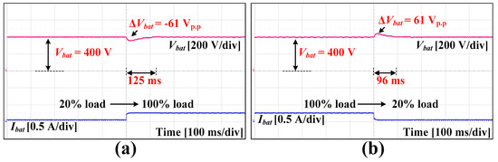
Figure 13.
Transient responses of Vbat while changing the battery load (a) from 20% to 100% and (b) from 100% to 20%.
To show that the proposed converter can operate both when charging the battery and when charging wirelessly, Vwpt and Vbat of the proposed converter were measured under the following four conditions (Figure 14): (1) Pwpt = 20 W and Pbat = 20 W, (2) Pwpt = 20 W and Pbat = 100 W, (3) Pwpt = 100 W and Pbat = 20 W, and (4) Pwpt = 100 W and Pbat = 100 W. Figure 14 shows that Vwpt decreases and Vbat increases when the power (Pwpt, Pbat) increases. However, both Vwpt and Vbat maintained a near fixed value; Vwpt changed from 183.8 to 180.9 V, which is just a 1.58% change, and Vbat changed from 399.8 to 401 V, which is just a 0.3% change.
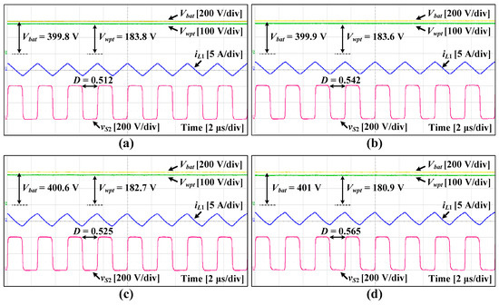
Figure 14.
The WPT voltage (Vwpt) and the battery voltage (Vbat) measured at (a) Pwpt = 20 W and Pbat = 20 W, (b) Pwpt = 20 W and Pbat = 100 W, (c) Pwpt = 100 W and Pbat = 20 W, and (d) Pwpt = 100 W and Pbat = 100 W.
The measured Vwpt and Vbat are summarized in Table 2, and this experimental result shows that the proposed converter can operate in both charging the battery and charging wirelessly because both Vwpt and Vbat maintain a near fixed value regardless of Pwpt and Pbat.
Table 2.
WPT and battery voltages according to the WPT and battery powers.
4. Conclusions
This paper presented a three-port converter to integrate an ES system with a WPT system. If the ES and WPT systems are used separately, many converters are needed. However, these ES and WPT systems can be integrated through only one proposed converter because the proposed converter can use an inductor in the bidirectional DC-DC converter as a transmitting coil for the WPT system. Therefore, the proposed converter consists only of a bidirectional DC-DC converter and an AC-DC converter, and an ES-WPT system that uses the proposed converter can minimize the cost and circuit size. The operation of the proposed converter was verified by theoretical analysis and experimental results, and the proposed converter had high ηe,wpt > 82% for 20 W ≤ Pwpt ≤ 100 W, and ηe,bat > 83% for 20 W ≤ Pbat ≤ 100 W, due to the ZVS turn-on of all switches. These results show that the proposed converter is suitable for the ES-WPT system that is part of future PV energy delivery and management infrastructure for residential applications.
Author Contributions
Both authors contributed equally to this work. H.-S.L. presented the main idea of the three-port converter. H.-S.L. and J.-J.Y. analyzed the proposed converter and performed experiments. J.-J.Y. contributed to the overall composition and writing of the manuscript. All authors have read and agreed to the published version of the manuscript.
Funding
This work was supported by the National Research Foundation of Korea (NRF) grant funded by the government of Korea (MSIP) (NRF-2018R1A1A1A05079496).
Conflicts of Interest
The authors have no conflict of interest.
References
- Malinowski, M.; Leon, J.I.; Abu-Rub, H. Solar photovoltaic and thermal energy systems: Current technology and future trends. Proc. IEEE 2017, 105, 2132–2146. [Google Scholar] [CrossRef]
- Kroposki, B.; Johnson, B.; Zhang, Y.; Gevorgian, V.; Denholm, P.; Hodge, B.-M.; Hannegan, B. Achieving a 100% renewable grid: Operating electric power systems with extremely high levels of variable renewable energy. IEEE Power Energy Mag. 2017, 15, 61–73. [Google Scholar] [CrossRef]
- Sahu, B.K. A study on global solar PV energy developments and policies with special focus on the top ten solar PV power producing countries. Renew. Sustain. Energy Rev. 2015, 43, 621–634. [Google Scholar] [CrossRef]
- McElroy, M.B.; Chen, X. Wind and solar power in the United States: Status and prospects. CSEE J. Power Energy Syst. 2017, 3, 1–6. [Google Scholar] [CrossRef]
- Park, L.; Jang, Y.; Cho, S.; Kim, J. Residential Demand Response for Renewable Energy Resources in Smart Grid Systems. IEEE Trans. Ind. Inf. 2017, 13, 3165–3173. [Google Scholar] [CrossRef]
- Chaudhari, K.; Ukil, A.; Kumar, K.N.; Manandhar, U.; Kollimalla, S.K. Hybrid Optimization for Economic Deployment of ESS in PV-Integrated EV Charging Stations. IEEE Trans. Ind. Inf. 2018, 14, 106–116. [Google Scholar] [CrossRef]
- Liu, X.; Aichhorn, A.; Liu, L.; Li, H. Coordinated Control of Distributed Energy Storage System with Tap Changer Transformers for Voltage Rise Mitigation Under High Photovoltaic Penetration. IEEE Trans. Smart Grid 2012, 3, 897–906. [Google Scholar] [CrossRef]
- Park, J.; Kim, D.; Hwang, K.; Park, H.H.; Kwak, S.I.; Kwon, J.H.; Ahn, S. A Resonant Reactive Shielding for Planar Wireless Power Transfer System in Smartphone Application. IEEE Trans. Electromagn. Compat. 2017, 59, 695–703. [Google Scholar] [CrossRef]
- Jeong, N.S.; Carobolante, F. Enabling Wireless Power Transfer Though a Metal Encased Handheld Device. In Proceedings of the IEEE Wireless Power Transfer Conference, Aveiro, Portugal, 5–6 May 2016. [Google Scholar]
- Nguyen, V.T.; Kang, S.H.; Choi, J.H.; Jung, C.W. Magnetic Resonance Wireless Power Transfer using Three-Coil System with Single Planar Receiver for Laptop Applications. IEEE Trans. Consum. Electron. 2015, 61, 160–166. [Google Scholar] [CrossRef]
- Barman, S.D.; Reza, A.W.; Kumar, N.; Karim, M.E.; Munir, A.B. Wireless powering by magnetic resonant coupling: Recent trends in wireless power transfer system and its applications. Renew. Sustain. Energy Rev. 2015, 51, 1525–1552. [Google Scholar] [CrossRef]
- Chen, Y.M.; Huang, A.Q.; Yu, X. A High Step-Up Three-Port DC–DC Converter for Stand-Alone PV/Battery Power Systems. IEEE Trans. Power Electron. 2013, 28, 5049–5062. [Google Scholar] [CrossRef]
- Phattanasak, M.; Gavagsaz-Ghoachani, R.; Martin, J.P.; Nahid-Mobarakeh, B.; Pierfederici, S.; Davat, B. Control of a Hybrid Energy Source Comprising a Fuel Cell and Two Storage Devices Using Isolated Three-Port Bidirectional DC–DC Converters. IEEE Trans. Ind. Appl. 2015, 51, 491–497. [Google Scholar] [CrossRef]
- Wang, P.; Lu, X.; Wang, W.; Xu, D. Frequency Division Based Coordinated Control of Three-Port Converter Interfaced Hybrid Energy Storage Systems in Autonomous DC Microgrids. IEEE Access 2018, 6, 25389–25398. [Google Scholar] [CrossRef]
- Duarte, J.L.; Hendrix, M.; Simoes, M.G. Three-Port Bidirectional Converter for Hybrid Fuel Cell Systems. IEEE Trans. Power Electron. 2007, 22, 480–487. [Google Scholar] [CrossRef]
- Wang, Z.; Li, H. An Integrated Three-Port Bidirectional DC–DC Converter for PV Application on a DC Distribution System. IEEE Trans. Power Electron. 2013, 28, 4612–4624. [Google Scholar] [CrossRef]
- Mira, M.C.; Zhang, Z.; Knott, A.; Andersen, M.A.E. Analysis, Design, Modeling, and Control of an Interleaved-Boost Full-Bridge Three-Port Converter for Hybrid Renewable Energy Systems. IEEE Trans. Power Electron. 2017, 32, 1138–1155. [Google Scholar] [CrossRef]
- Zhang, J.; Wu, H.; Qin, X.; Xing, Y. PWM Plus Secondary-Side Phase-Shift Controlled Soft-Switching Full-Bridge Three-Port Converter for Renewable Power Systems. IEEE Trans. Ind. Electron. 2015, 62, 7061–7072. [Google Scholar] [CrossRef]
- Hesterman, B. Analysis and Modeling of Magnetic Coupling. Denver Chapter, IEEE Power Electronics Society. 2007, pp. 35–38. Available online: http://www.verimod.com/presentations/Denver_PELS_20070410_Hesterman_Magnetic_Coupling.pdf (accessed on 16 December 2019).
- Zhu, G.; McDonald, B.A.; Wang, K. Modeling and Analysis of Coupled Inductors in Power Converters. IEEE Trans. Power Electron. 2011, 26, 1355–1363. [Google Scholar] [CrossRef]
- Dai, J.; Ludois, D.C. A Survey of Wireless Power Transfer and a Critical Comparison of Inductive and Capacitive Coupling for Small Gap Applications. IEEE Trans. Power Electron. 2015, 30, 6017–6029. [Google Scholar] [CrossRef]
- Xu, H.; Wang, C.; Xia, D.; Liu, Y. Design of Magnetic Coupler for Wireless Power Transfer. Energies 2019, 12, 3000. [Google Scholar] [CrossRef]
- Dayerizadeh, A.; Lukic, S. Saturable inductors for superior reflexive field containment in inductive power transfer systems. In Proceedings of the IEEE Applied Power Electronics Conference and Exposition (APEC), San Antonio, TX, USA, 4–8 March 2018. [Google Scholar]
- McLyman, W.T. Transformer and Inductor Design Handbook, 3rd ed.; Marcel Dekker, Inc.: New York, NY, USA, 2004. [Google Scholar]
- Mohan, N.; Undeland, T.M. Power Electronics: Converters, Applications, and Design; John Wiley & Sons: Hoboken, NJ, USA, 2007. [Google Scholar]
- Orenchak, G.G. Specify Saturation Properties of Ferrite Cores to Prevent Field Failure. Available online: http://www.tscinternational.com/tech13.pdf (accessed on 16 December 2019).
- Itoh, Y.; Hattori, F.; Kimura, S.; Imaoka, J.; Yamamoto, M. Design method considering magnetic saturation issue of coupled inductor in interleaved CCM boost PFC converter. In Proceedings of the IEEE Energy Conversion Congress and Exposition (ECCE), Montreal, QC, Canada, 20–24 September 2015. [Google Scholar]


© 2020 by the authors. Licensee MDPI, Basel, Switzerland. This article is an open access article distributed under the terms and conditions of the Creative Commons Attribution (CC BY) license (http://creativecommons.org/licenses/by/4.0/).