Three-Port Converter for Integrating Energy Storage and Wireless Power Transfer Systems in Future Residential Applications


Abstract
:1. Introduction
2. Proposed Three-Port Converter
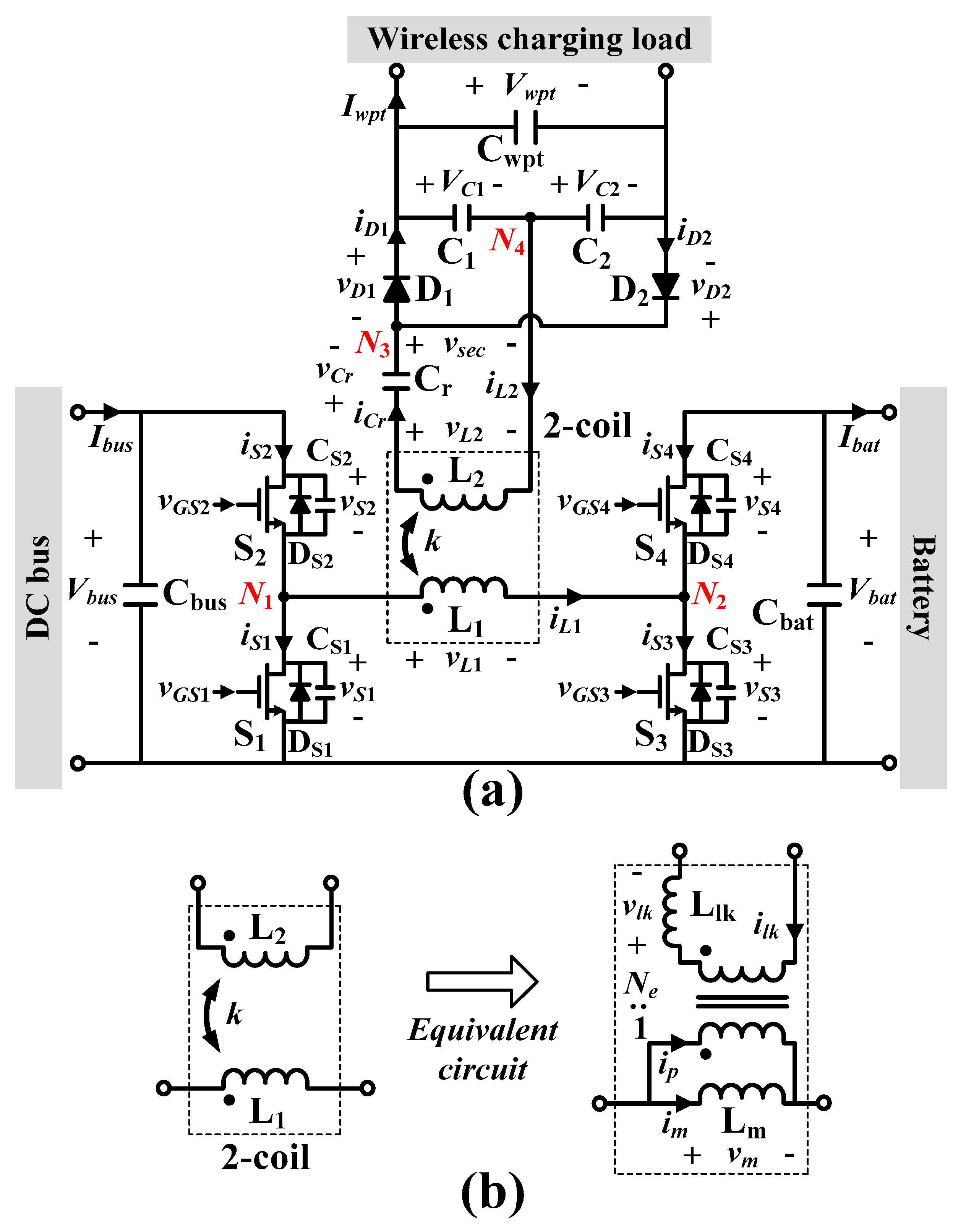
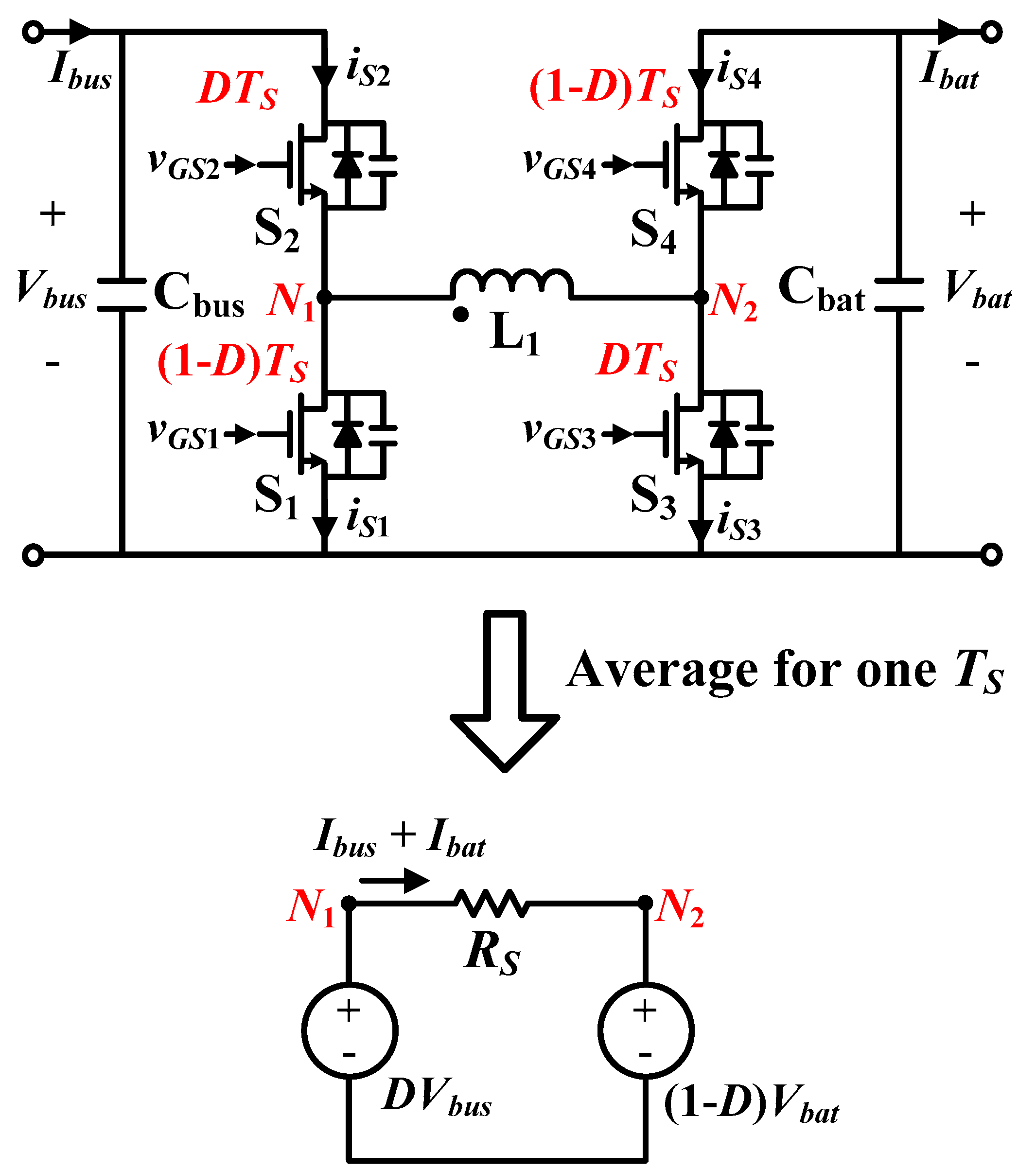
2.1. Circuit Structure
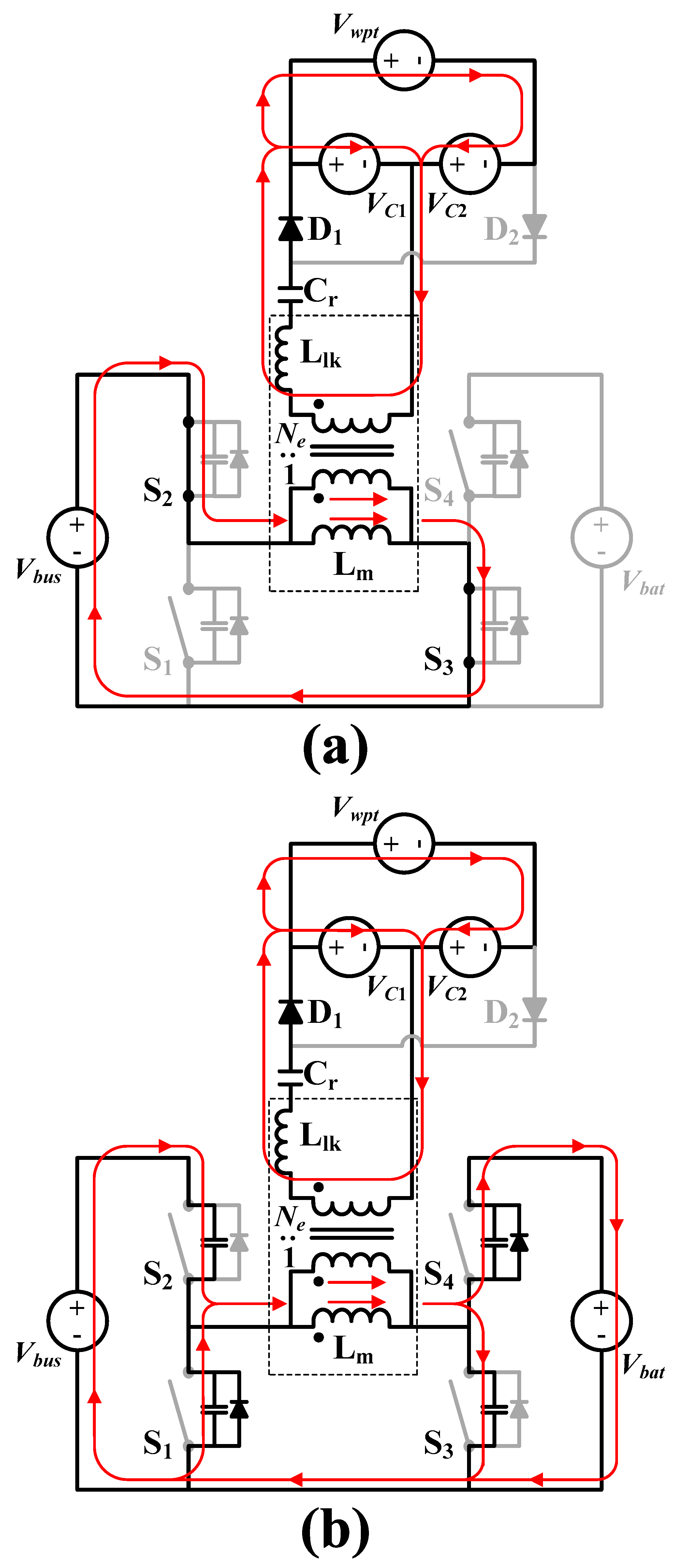
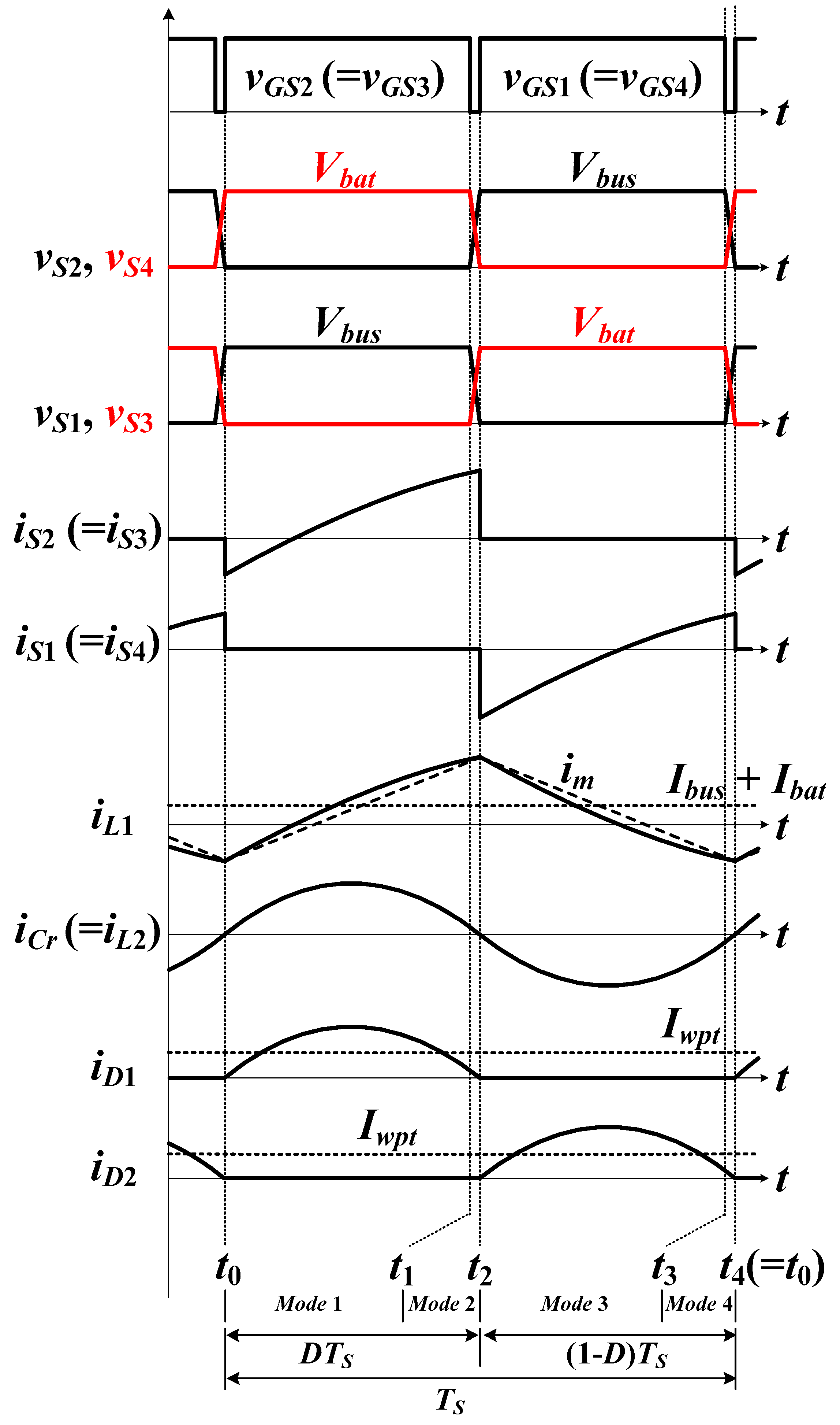
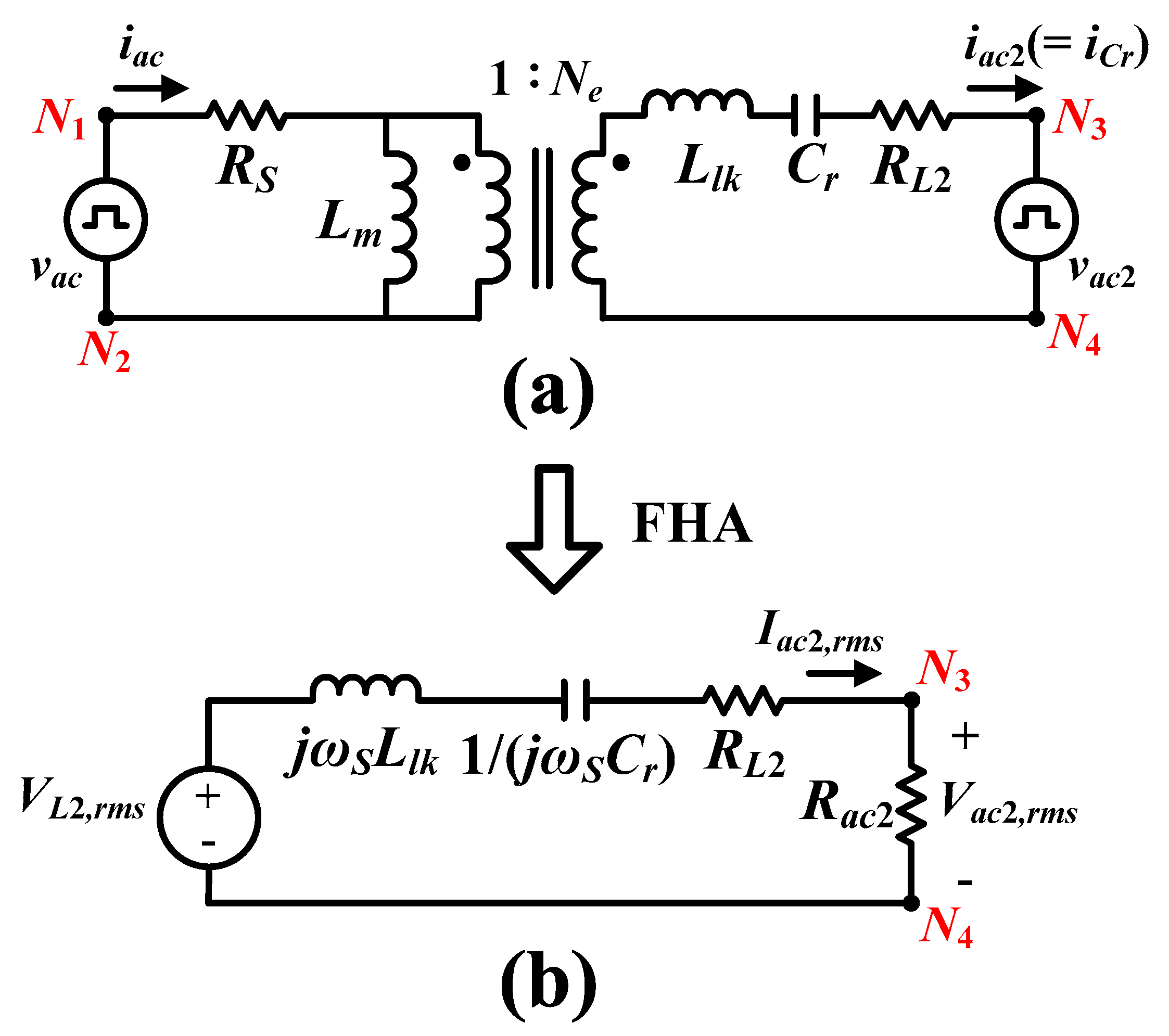
2.2. Principle of Operation
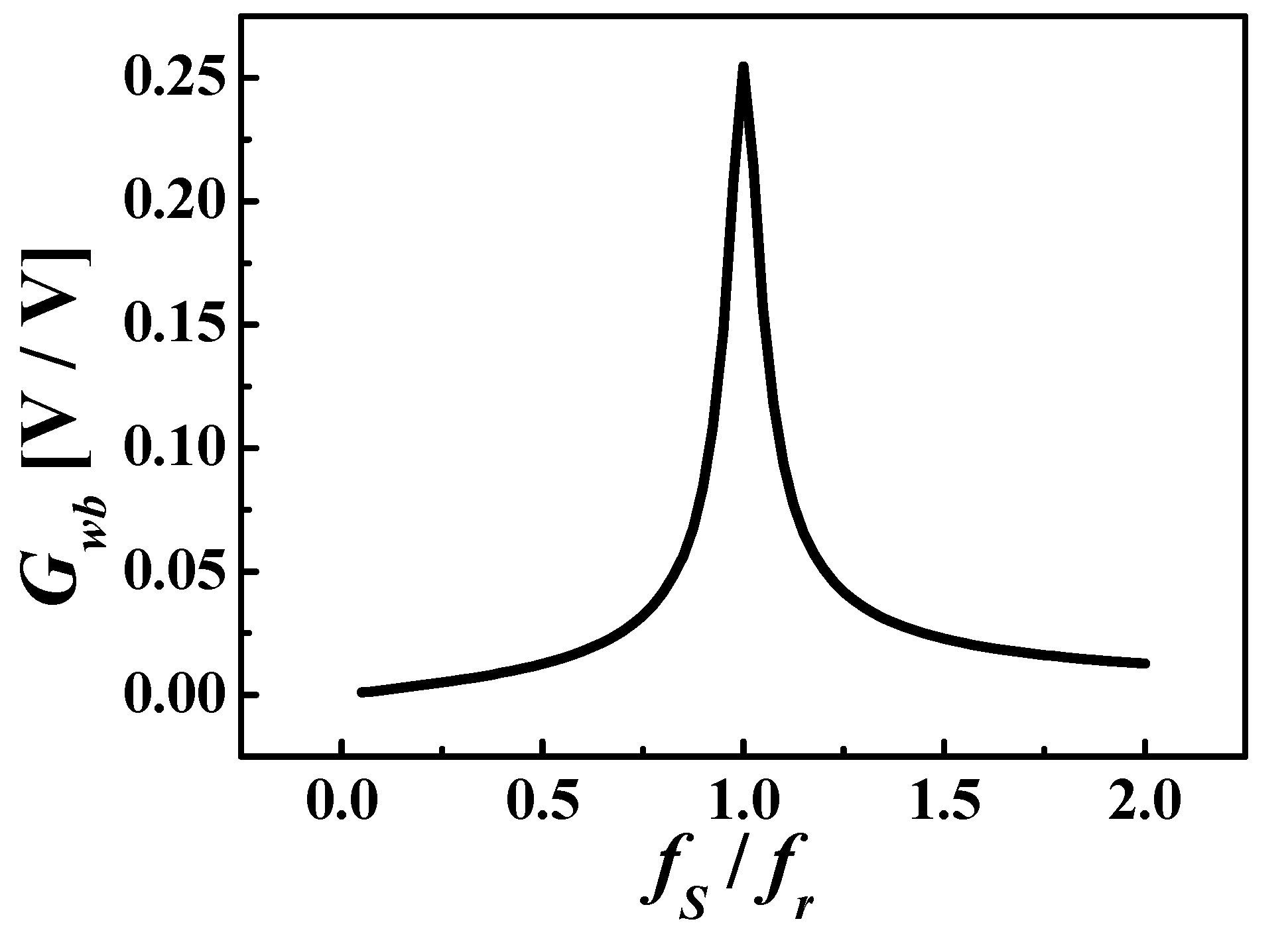
2.3. Voltage Gain
2.4. Magnetic Saturation
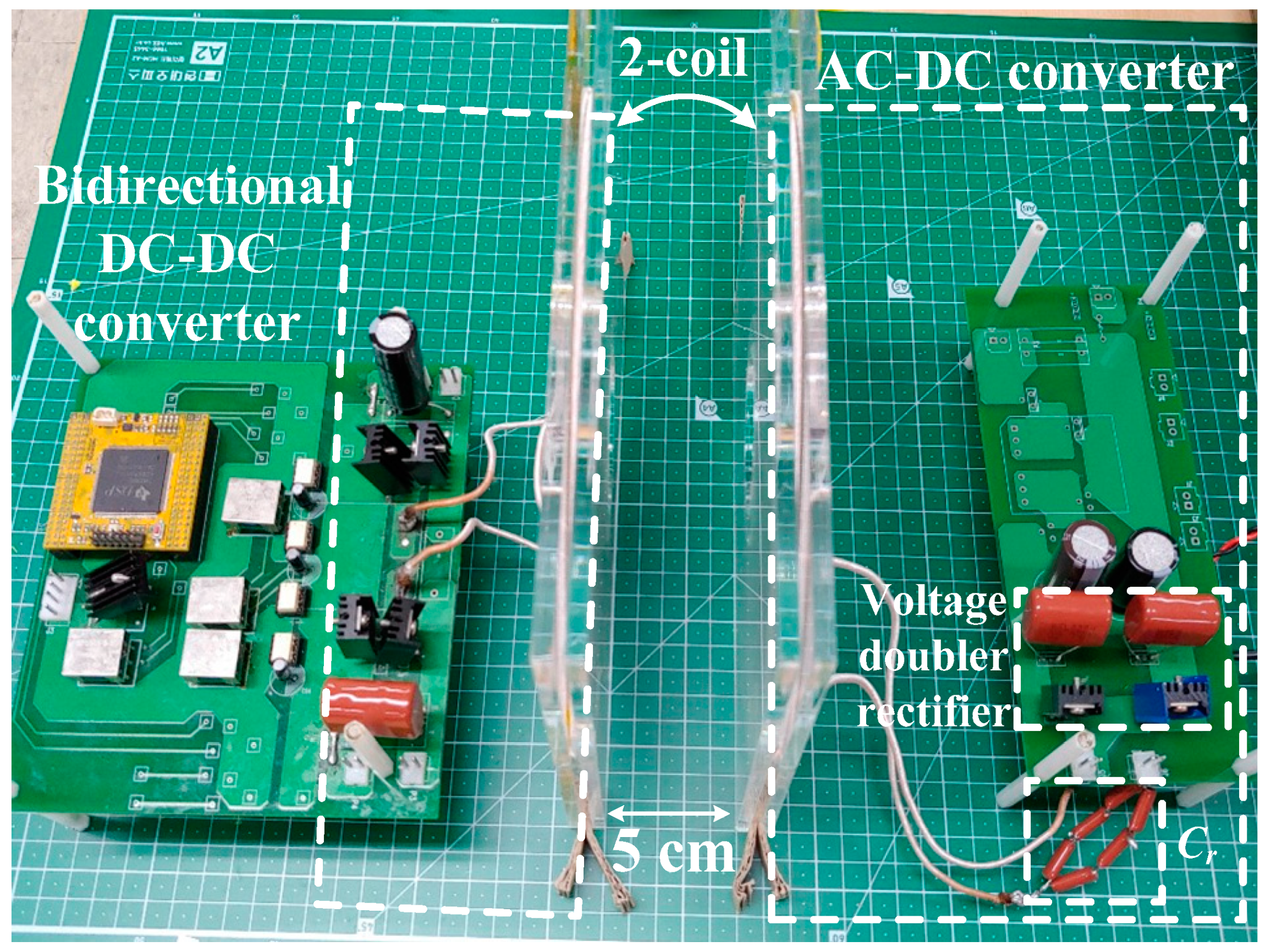
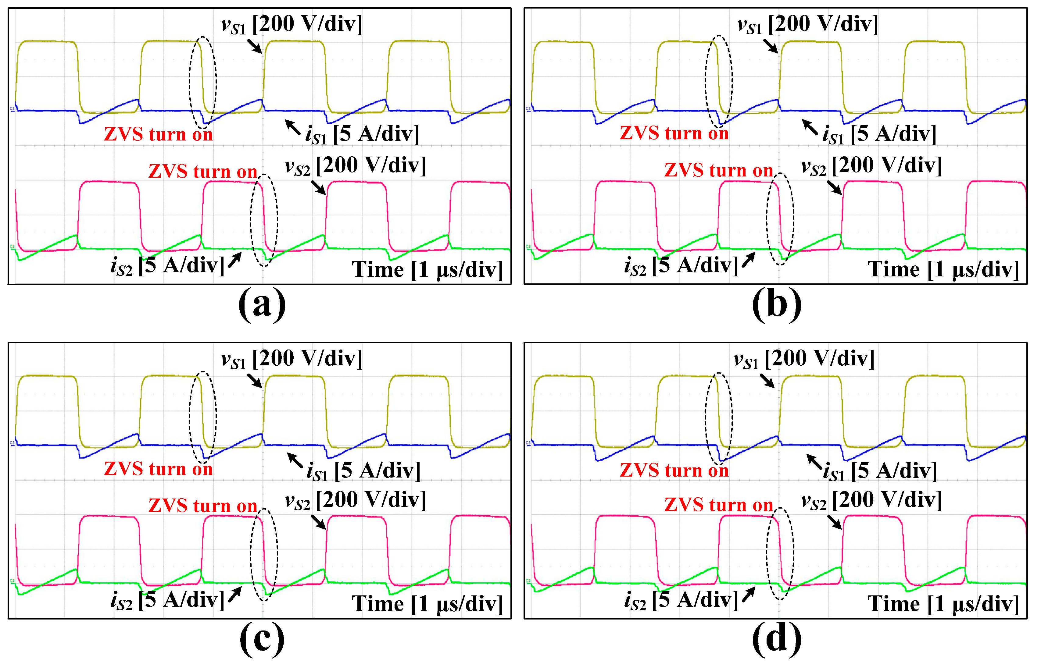
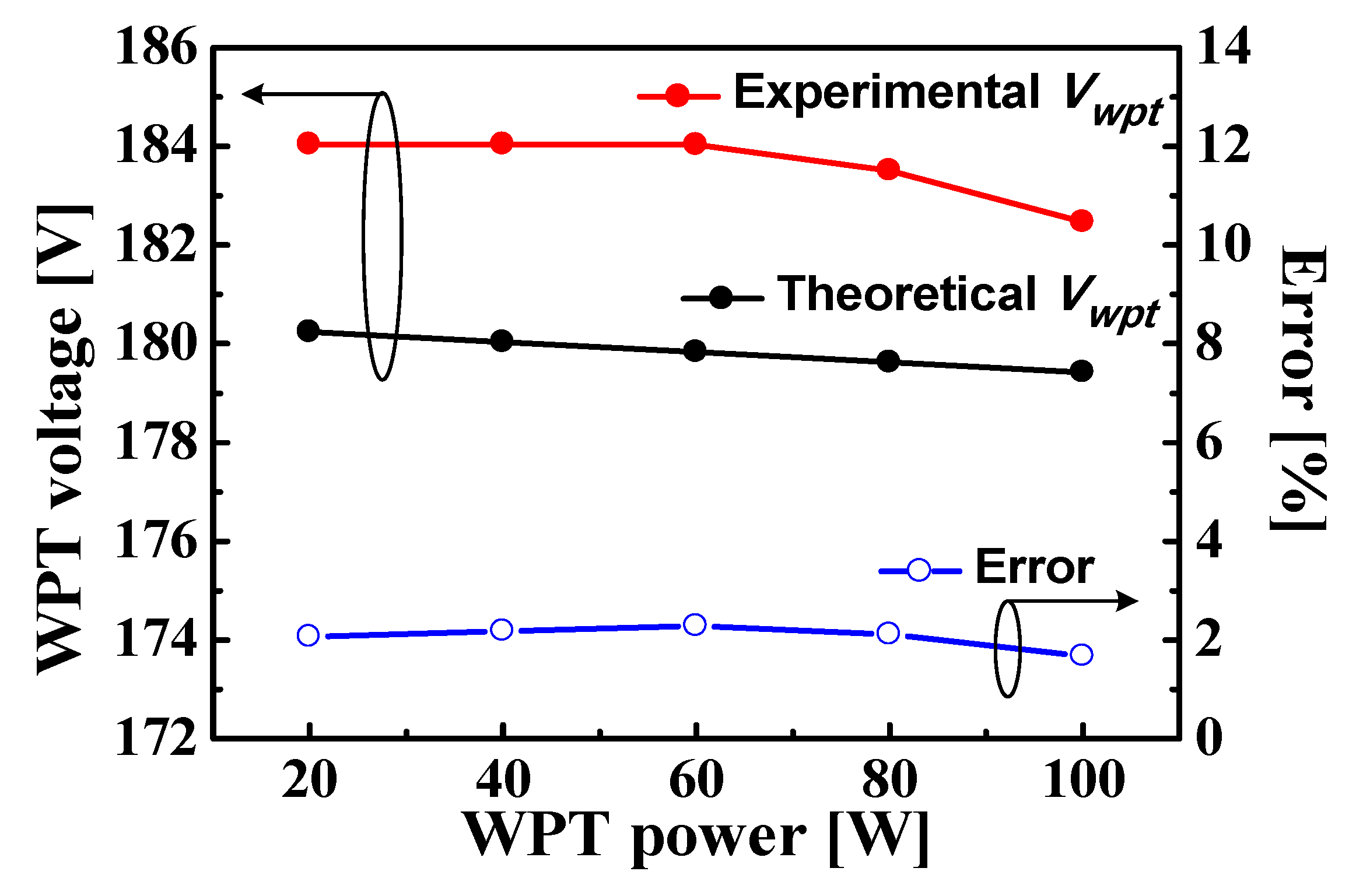
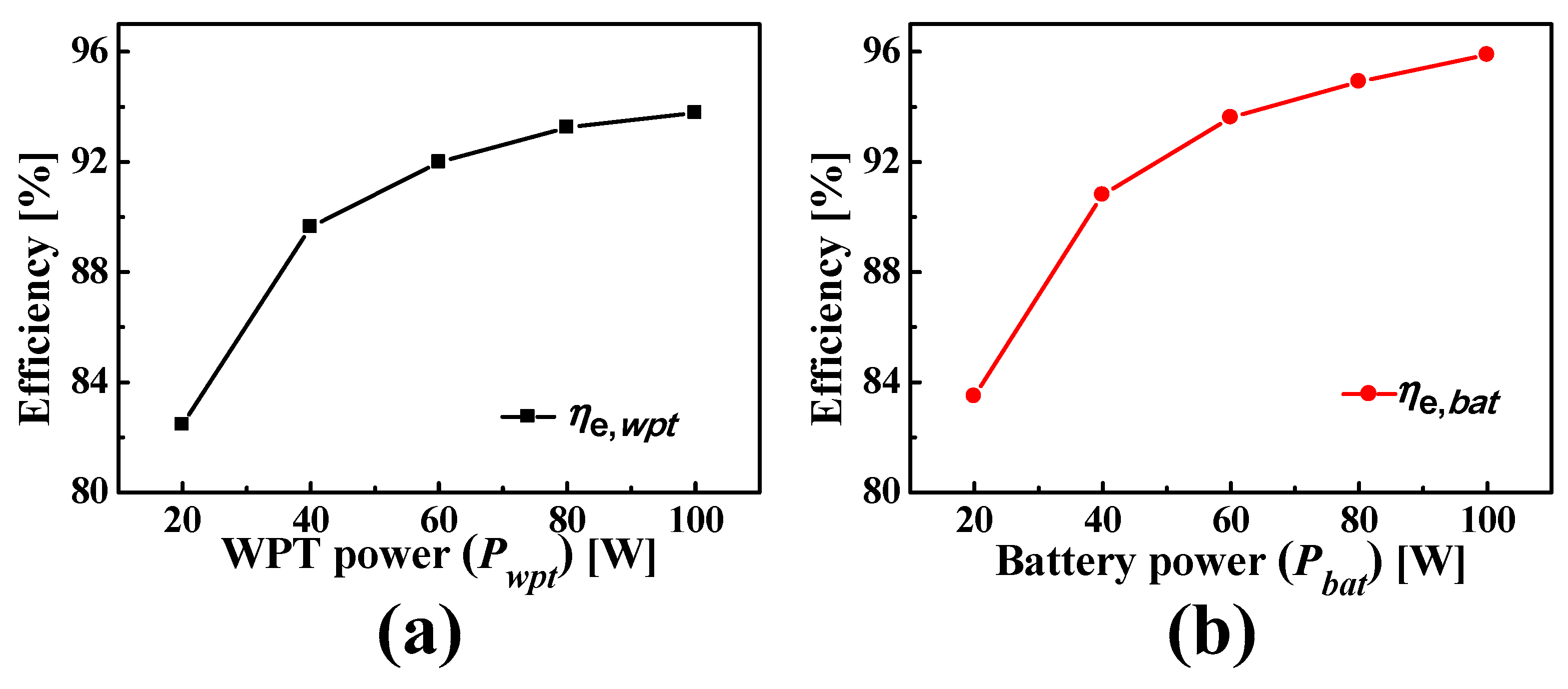
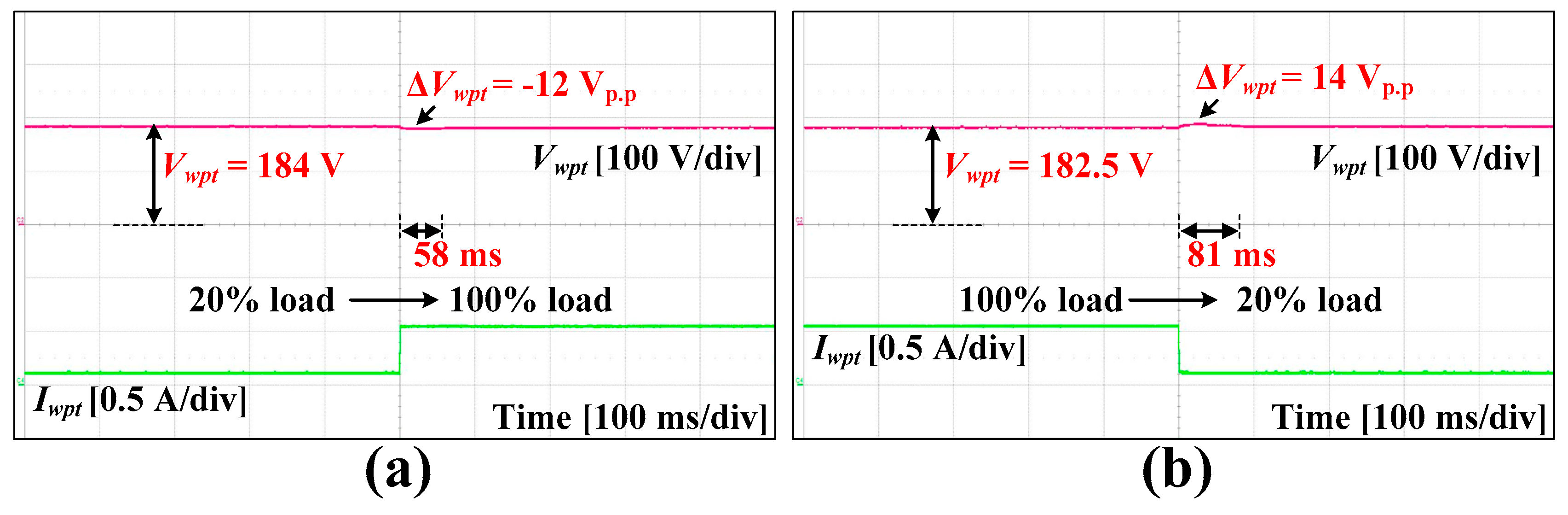
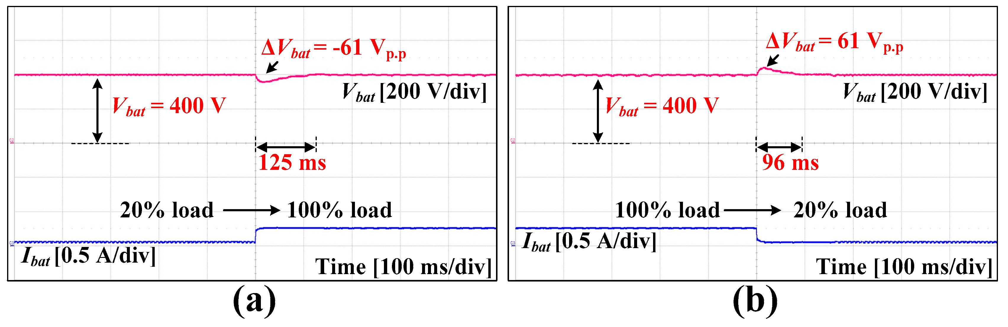
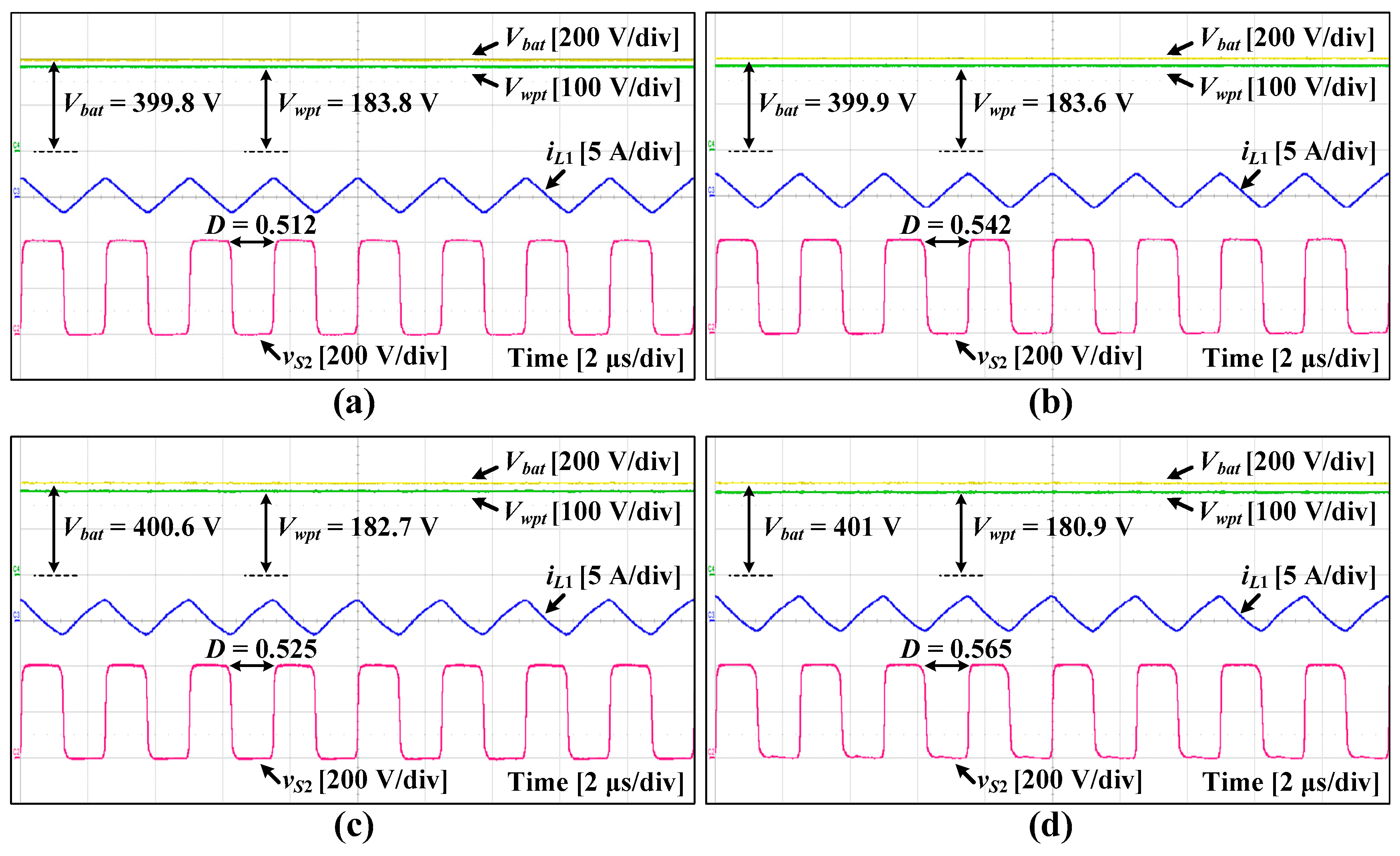
3. Experimental Results
4. Conclusions
Author Contributions
Funding
Conflicts of Interest
References
- Malinowski, M.; Leon, J.I.; Abu-Rub, H. Solar photovoltaic and thermal energy systems: Current technology and future trends. Proc. IEEE 2017, 105, 2132–2146. [Google Scholar] [CrossRef]
- Kroposki, B.; Johnson, B.; Zhang, Y.; Gevorgian, V.; Denholm, P.; Hodge, B.-M.; Hannegan, B. Achieving a 100% renewable grid: Operating electric power systems with extremely high levels of variable renewable energy. IEEE Power Energy Mag. 2017, 15, 61–73. [Google Scholar] [CrossRef]
- Sahu, B.K. A study on global solar PV energy developments and policies with special focus on the top ten solar PV power producing countries. Renew. Sustain. Energy Rev. 2015, 43, 621–634. [Google Scholar] [CrossRef]
- McElroy, M.B.; Chen, X. Wind and solar power in the United States: Status and prospects. CSEE J. Power Energy Syst. 2017, 3, 1–6. [Google Scholar] [CrossRef]
- Park, L.; Jang, Y.; Cho, S.; Kim, J. Residential Demand Response for Renewable Energy Resources in Smart Grid Systems. IEEE Trans. Ind. Inf. 2017, 13, 3165–3173. [Google Scholar] [CrossRef]
- Chaudhari, K.; Ukil, A.; Kumar, K.N.; Manandhar, U.; Kollimalla, S.K. Hybrid Optimization for Economic Deployment of ESS in PV-Integrated EV Charging Stations. IEEE Trans. Ind. Inf. 2018, 14, 106–116. [Google Scholar] [CrossRef]
- Liu, X.; Aichhorn, A.; Liu, L.; Li, H. Coordinated Control of Distributed Energy Storage System with Tap Changer Transformers for Voltage Rise Mitigation Under High Photovoltaic Penetration. IEEE Trans. Smart Grid 2012, 3, 897–906. [Google Scholar] [CrossRef]
- Park, J.; Kim, D.; Hwang, K.; Park, H.H.; Kwak, S.I.; Kwon, J.H.; Ahn, S. A Resonant Reactive Shielding for Planar Wireless Power Transfer System in Smartphone Application. IEEE Trans. Electromagn. Compat. 2017, 59, 695–703. [Google Scholar] [CrossRef]
- Jeong, N.S.; Carobolante, F. Enabling Wireless Power Transfer Though a Metal Encased Handheld Device. In Proceedings of the IEEE Wireless Power Transfer Conference, Aveiro, Portugal, 5–6 May 2016. [Google Scholar]
- Nguyen, V.T.; Kang, S.H.; Choi, J.H.; Jung, C.W. Magnetic Resonance Wireless Power Transfer using Three-Coil System with Single Planar Receiver for Laptop Applications. IEEE Trans. Consum. Electron. 2015, 61, 160–166. [Google Scholar] [CrossRef]
- Barman, S.D.; Reza, A.W.; Kumar, N.; Karim, M.E.; Munir, A.B. Wireless powering by magnetic resonant coupling: Recent trends in wireless power transfer system and its applications. Renew. Sustain. Energy Rev. 2015, 51, 1525–1552. [Google Scholar] [CrossRef]
- Chen, Y.M.; Huang, A.Q.; Yu, X. A High Step-Up Three-Port DC–DC Converter for Stand-Alone PV/Battery Power Systems. IEEE Trans. Power Electron. 2013, 28, 5049–5062. [Google Scholar] [CrossRef]
- Phattanasak, M.; Gavagsaz-Ghoachani, R.; Martin, J.P.; Nahid-Mobarakeh, B.; Pierfederici, S.; Davat, B. Control of a Hybrid Energy Source Comprising a Fuel Cell and Two Storage Devices Using Isolated Three-Port Bidirectional DC–DC Converters. IEEE Trans. Ind. Appl. 2015, 51, 491–497. [Google Scholar] [CrossRef]
- Wang, P.; Lu, X.; Wang, W.; Xu, D. Frequency Division Based Coordinated Control of Three-Port Converter Interfaced Hybrid Energy Storage Systems in Autonomous DC Microgrids. IEEE Access 2018, 6, 25389–25398. [Google Scholar] [CrossRef]
- Duarte, J.L.; Hendrix, M.; Simoes, M.G. Three-Port Bidirectional Converter for Hybrid Fuel Cell Systems. IEEE Trans. Power Electron. 2007, 22, 480–487. [Google Scholar] [CrossRef] [Green Version]
- Wang, Z.; Li, H. An Integrated Three-Port Bidirectional DC–DC Converter for PV Application on a DC Distribution System. IEEE Trans. Power Electron. 2013, 28, 4612–4624. [Google Scholar] [CrossRef]
- Mira, M.C.; Zhang, Z.; Knott, A.; Andersen, M.A.E. Analysis, Design, Modeling, and Control of an Interleaved-Boost Full-Bridge Three-Port Converter for Hybrid Renewable Energy Systems. IEEE Trans. Power Electron. 2017, 32, 1138–1155. [Google Scholar] [CrossRef] [Green Version]
- Zhang, J.; Wu, H.; Qin, X.; Xing, Y. PWM Plus Secondary-Side Phase-Shift Controlled Soft-Switching Full-Bridge Three-Port Converter for Renewable Power Systems. IEEE Trans. Ind. Electron. 2015, 62, 7061–7072. [Google Scholar] [CrossRef]
- Hesterman, B. Analysis and Modeling of Magnetic Coupling. Denver Chapter, IEEE Power Electronics Society. 2007, pp. 35–38. Available online: http://www.verimod.com/presentations/Denver_PELS_20070410_Hesterman_Magnetic_Coupling.pdf (accessed on 16 December 2019).
- Zhu, G.; McDonald, B.A.; Wang, K. Modeling and Analysis of Coupled Inductors in Power Converters. IEEE Trans. Power Electron. 2011, 26, 1355–1363. [Google Scholar] [CrossRef]
- Dai, J.; Ludois, D.C. A Survey of Wireless Power Transfer and a Critical Comparison of Inductive and Capacitive Coupling for Small Gap Applications. IEEE Trans. Power Electron. 2015, 30, 6017–6029. [Google Scholar] [CrossRef]
- Xu, H.; Wang, C.; Xia, D.; Liu, Y. Design of Magnetic Coupler for Wireless Power Transfer. Energies 2019, 12, 3000. [Google Scholar] [CrossRef] [Green Version]
- Dayerizadeh, A.; Lukic, S. Saturable inductors for superior reflexive field containment in inductive power transfer systems. In Proceedings of the IEEE Applied Power Electronics Conference and Exposition (APEC), San Antonio, TX, USA, 4–8 March 2018. [Google Scholar]
- McLyman, W.T. Transformer and Inductor Design Handbook, 3rd ed.; Marcel Dekker, Inc.: New York, NY, USA, 2004. [Google Scholar]
- Mohan, N.; Undeland, T.M. Power Electronics: Converters, Applications, and Design; John Wiley & Sons: Hoboken, NJ, USA, 2007. [Google Scholar]
- Orenchak, G.G. Specify Saturation Properties of Ferrite Cores to Prevent Field Failure. Available online: http://www.tscinternational.com/tech13.pdf (accessed on 16 December 2019).
- Itoh, Y.; Hattori, F.; Kimura, S.; Imaoka, J.; Yamamoto, M. Design method considering magnetic saturation issue of coupled inductor in interleaved CCM boost PFC converter. In Proceedings of the IEEE Energy Conversion Congress and Exposition (ECCE), Montreal, QC, Canada, 20–24 September 2015. [Google Scholar]


| Components | Values | ||
|---|---|---|---|
| 2-coil structure | Winding type | Spiral | |
| Distance between two coils | 5 cm | ||
| Coupling coefficient (k) | 0.227 | ||
| Equivalent turn ratio (Ne) | 0.226 | ||
| Primary winding | Inductance (L1) | 117.5 µH | |
| Resistance (RL1) | 0.43 Ω | ||
| Turn number (N1) | 28 T | ||
| Secondary winding | Inductance (L2) | 116.5 µH | |
| Resistance (RL2) | 0.4 Ω | ||
| Turn number (N2) | 28 T | ||
| Resonant capacitor (Cr) | 1.43 nF | ||
| Doubler capacitors (C1, C2) | 2.2 µF | ||
| Switches (S1~S4) | FCP099N60E (Ron = 99 mΩ) | ||
| Diodes (D1, D2) | BYV29-500 | ||
| Power | WPT Power (Pwpt) | 20 W | 20 W | 100 W | 100 W |
|---|---|---|---|---|---|
| Battery Power (Pwpt) | 20 W | 100 W | 20 W | 100 W | |
| WPT voltage (Vwpt) | 183.8 V | 183.6 V | 182.7 V | 180.9 V | |
| Battery voltage (Vbat) | 399.8 V | 399.9 V | 400.6 V | 401 V | |
© 2020 by the authors. Licensee MDPI, Basel, Switzerland. This article is an open access article distributed under the terms and conditions of the Creative Commons Attribution (CC BY) license (http://creativecommons.org/licenses/by/4.0/).
Share and Cite
Lee, H.-S.; Yun, J.-J. Three-Port Converter for Integrating Energy Storage and Wireless Power Transfer Systems in Future Residential Applications. Energies 2020, 13, 272. https://doi.org/10.3390/en13010272
Lee H-S, Yun J-J. Three-Port Converter for Integrating Energy Storage and Wireless Power Transfer Systems in Future Residential Applications. Energies. 2020; 13(1):272. https://doi.org/10.3390/en13010272
Chicago/Turabian StyleLee, Hyeon-Seok, and Jae-Jung Yun. 2020. "Three-Port Converter for Integrating Energy Storage and Wireless Power Transfer Systems in Future Residential Applications" Energies 13, no. 1: 272. https://doi.org/10.3390/en13010272
APA StyleLee, H. -S., & Yun, J. -J. (2020). Three-Port Converter for Integrating Energy Storage and Wireless Power Transfer Systems in Future Residential Applications. Energies, 13(1), 272. https://doi.org/10.3390/en13010272