Article

Interleaved High Step-Up DC–DC Converter with Voltage-Lift and Voltage-Stack Techniques for Photovoltaic Systems †

1
Department of Electrical Engineering, Kun Shan University, Tainan 710303, Taiwan
2
Green Energy Technology Research Center, Kun Shan University, Tainan 710303, Taiwan
*
Author to whom correspondence should be addressed.
This present work is an extension of our paper “High step-up interleaved converter with three-winding coupled inductors and voltage multiplier cells” presented to IEEE ICIT 2019 conference, 13–15 February 2019, Melbourne, Australia.
Energies 2020, 13(10), 2537; https://doi.org/10.3390/en13102537
Submission received: 13 April 2020 / Revised: 11 May 2020 / Accepted: 14 May 2020 / Published: 16 May 2020
(This article belongs to the Special Issue Advanced DC-DC Power Converters and Switching Converters)

Abstract

:
A novel interleaved high step-up DC–DC converter applied for applications in photovoltaic systems is proposed in this paper. The proposed configuration is composed of three-winding coupled inductors, voltage multiplier cells and a clamp circuit. The step-up voltage gain is effectively increased, owing to the voltage-stack and voltage-lift techniques using the voltage multiplier cells. The leakage inductor energy is recycled by the clamp circuit to avoid the voltage surge on a power switch. The low-voltage-rated power switches with low on-state resistances and costs can be used to decrease the conduction losses and increase the conversion efficiency when the voltage stresses of power switches for the converter are considerably lower than the high output voltage. The reverse-recovery problems of diodes are mitigated by the leakage inductances of the coupled inductors. Moreover, both the input current ripple and the current stress on each power switch are reduced, owing to the interleaved operation. The operating principle and steady-state analysis of the proposed converter are thoroughly presented herein. A controller network is designed to diminish the effect of the variations of input voltage and output load on the output voltage. Finally, the experimental results for a 1 kW prototype with 28–380 V voltage conversion are shown to demonstrate its effectiveness and performance.

1. Introduction

Because of the fast exhaustion of fossil fuels and the global warming problem, much research has been developed to cope with green energy sources, such as the fuel cells, photovoltaic power (PV power) or wind power. Generally, a single-phase 220 Vac grid-connected photovoltaic system requires a DC bus voltage of 380–420 V to provide the requirement for a full-bridge DC–AC inverter. Regrettably, the output voltages of individual PV modules are ordinarily lower than 40 V in household applications [1]. Thus, a high step-up DC–DC converter is necessary to serve as a voltage boosting cell between the PV modules and the AC power generation unit [2,3,4].
For a traditional boost converter, an extreme duty ratio operation has to be realized to obtain a high voltage gain. However, it will result in large current ripples, high conduction losses, reverse-recovery problems for diodes, and electromagnetic interference problems [5]. In addition, the voltage stresses on the power switches and diodes are equal to the high output voltage. Thus, high-voltage-rated MOSFETs with high on-state resistance and diodes with high forward voltage drop should be used, which leads to lower efficiency due to high conduction losses. To proceed, isolated power converters, such as a conventional flyback DC–DC converter, can derive a high voltage gain by adopting a high transformer turns ratio, which results in a large leakage inductance. A large leakage inductance will cause a much higher voltage spike on the power switch and more power dissipations. Consequently, the aforementioned converters are not proper for use in a high step-up voltage gain application.
To overcome the above problems in high voltage gain applications, many high step-up converters have been presented in the literature. Coupled inductors have been adopted to obtain a high voltage gain in the non-isolated converters, because the turns ratio can be served as a control freedom to enlarge the voltage gain [6,7,8,9,10]. Recently, a three-winding coupled inductor has also been applied to a lot of high step-up DC–DC converters to achieve higher voltage gains [11,12,13]. In [14,15,16,17,18,19], the switched-inductor and/or switched-capacitor step-up converters are presented to derive a high voltage gain, owing to their simpler structure and operation. A double-duty technique was applied in the high step-up voltage gain applications with two distinct duty ratios for the power switches in [20,21]. The parallel structure on the input side with interleaved operation can be utilized to increase the power level and reduce the input current ripple. The voltage multiplier cells were also applied to the interleaved high step-up converters in [22,23,24]. The built-in transformer technique for obtaining a high step-up conversion ratio is presented in [25,26,27]. The interleaved DC–DC converters with three-winding coupled inductors in [28,29,30] exhibited a high voltage gain and better current sharing performance simultaneously.
An IA novel interleaved high step-up DC–DC converter is proposed in this paper. It contains three-winding coupled inductors, voltage multiplier cells and a clamp circuit. The voltage-stack and voltage-lift techniques are adopted to extend the voltage gain by means of the voltage multiplier cells. The clamp circuit is utilized to recycle the leakage inductor energy and clamp the voltage stress of power switches. The advantages of the proposed high step-up converter are as follows:
(1)
By designing a proper turns ratio for the coupled inductors, the high voltage conversion ratio can be obtained whilst operating at an appropriate duty ratio.
(2)
The voltage stresses on the power switches are greatly less than the output voltage, so the power switches with lower on-state resistances are utilized to decrease the conduction losses.
(3)
The power switches achieve zero-current switching at turn on, and the switching losses can thereby be reduced.
(4)
The diode reverse-recovery problem is effectively alleviated by the leakage inductances of the coupled inductors.
(5)
The leakage inductor energy can be recycled to suppress the voltage spikes on the power switches.
A prototype of 1 kW was implemented in the laboratory to verify the theoretical analysis and the performance of the proposed interleaved high step-up converter. The remainder of this paper is organized as follows. In Section 2, the circuit description is given, and the operating principle is presented in detail simultaneously. Section 3 shows the steady-state analysis. The performance comparison with existing converters is also presented. The closed-loop controller design is provided in Section 4. Section 5 provides the experimental results of a laboratory prototype. Finally, the conclusion of this paper is given in Section 6.

2. Circuit Description and Operating Principle

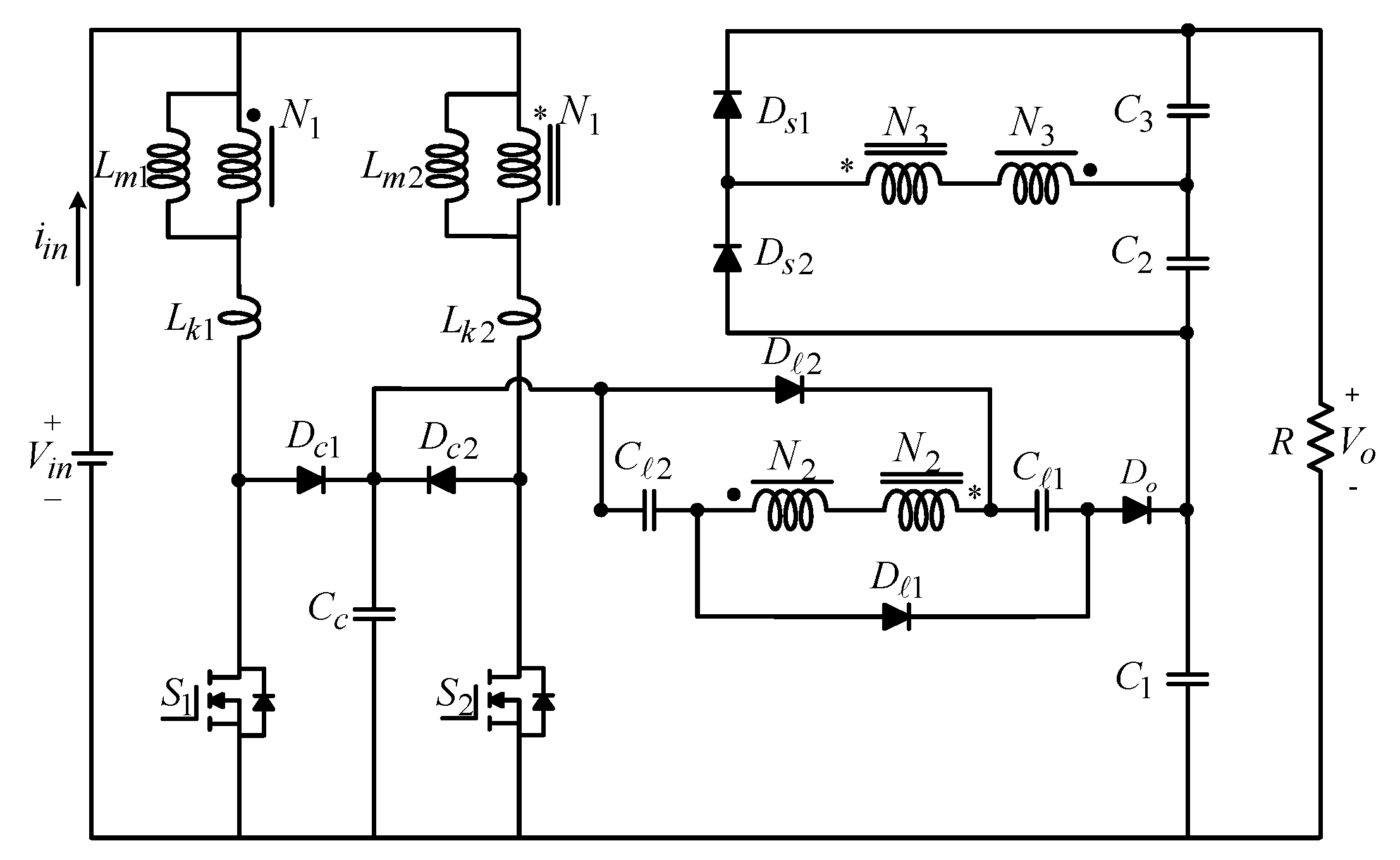
Figure 1 shows the circuit topology of the proposed converter. Two three-winding coupled inductors with the same number of turns are included in the proposed converter. The primary, secondary and tertiary windings are denoted by N 1 , N 2 and N 3 , respectively. The coupling reference is indicated by and . The primary windings are parallel connected to process the large input current and serve as the filter inductors in the conventional boost converter. The secondary windings are connected in series to constitute the voltage multiplier cell I, which is inserted between the clamp circuit and the output high voltage side to lift the output voltage. The tertiary windings are in series connection to constitute the voltage multiplier cell II, which is stacked on the output capacitor C 1 to enlarge the voltage conversion ratio.
The coupled inductor is modeled as an ideal transformer with a defined turns ratio, which is in parallel with a magnetizing inductor and in series with a leakage inductor. L m 1 and L m 2 represent the magnetizing inductances, while L k 1 and L k 2 represent the leakage inductances. Assuming that the number of turns N 3 is equal to N 2 . n is defined as the turns ratio with n = N 2 / N 1 = N 3 / N 1 . The equivalent circuit of the proposed converter is illustrated in Figure 2, where S 1 and S 2 are the power switches; D c 1 and D c 2 are the clamp diodes; C c is the clamp capacitor; D 1 and D 2 are the lift diodes; C 1 and C 2 are the lift capacitors; D s 1 and D s 2 are the switched diodes; C 1 , C 2 and C 3 are the output capacitors; D o is the output diode; V i n is the input voltage; V o is the output voltage; and R is the output load.
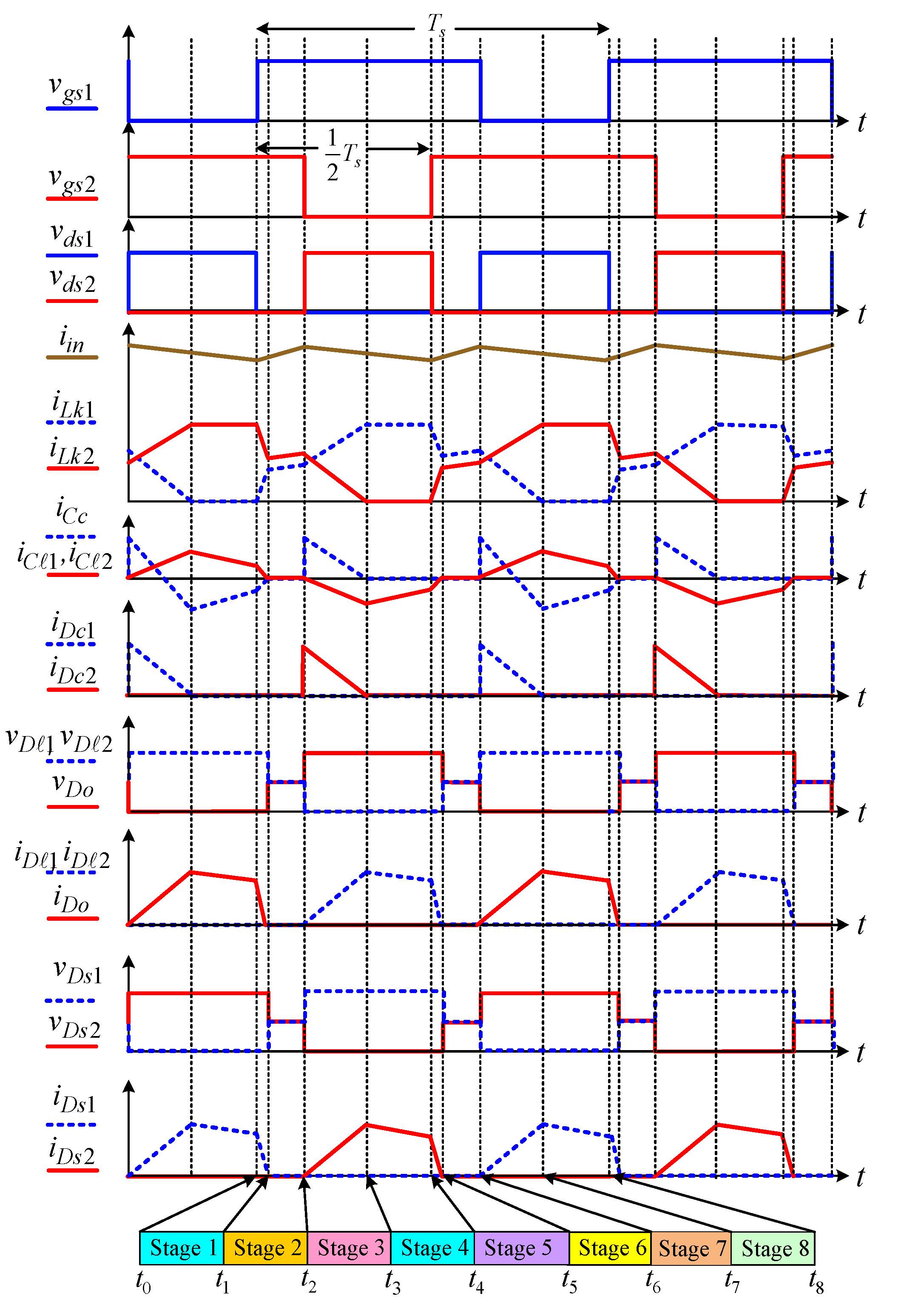
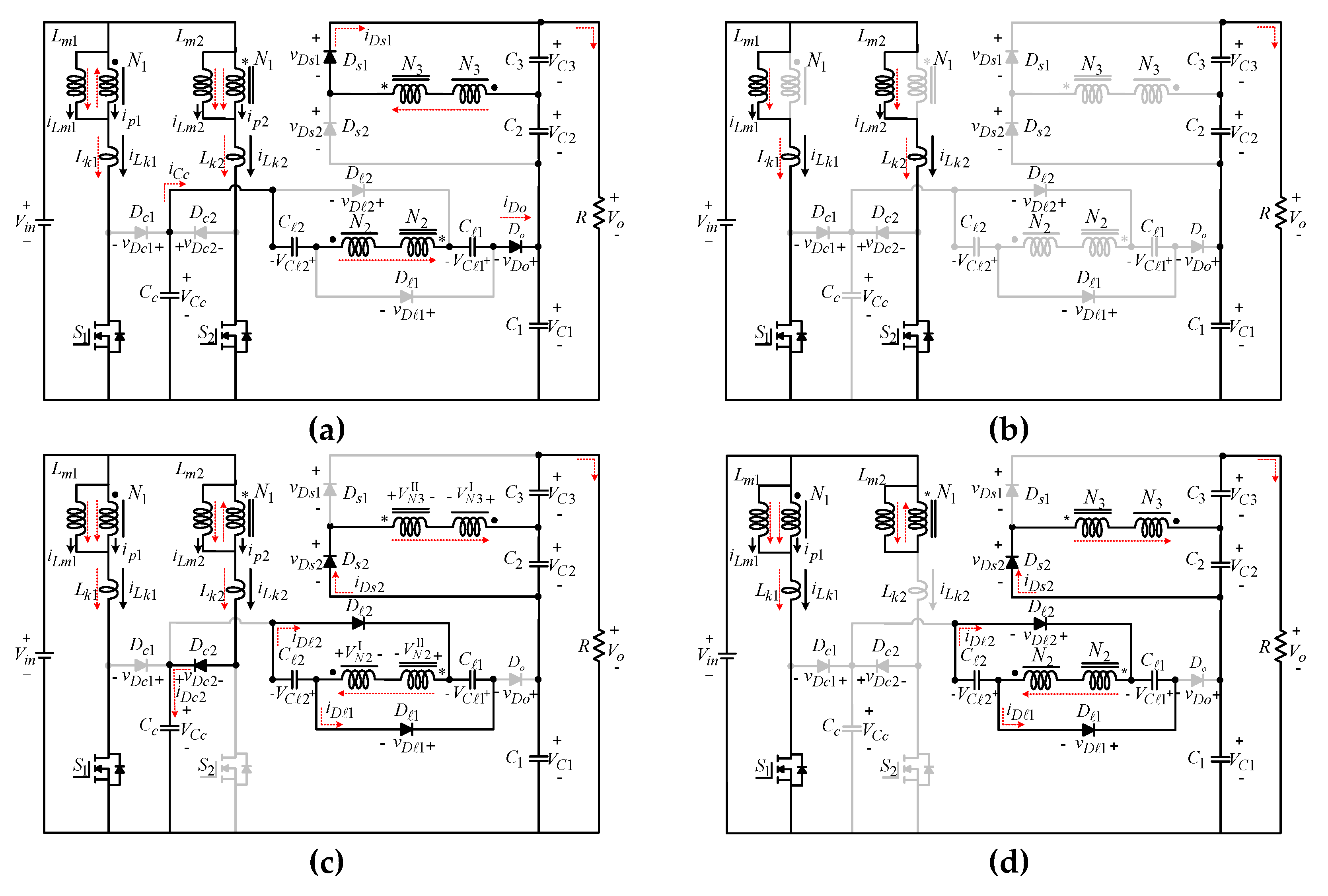
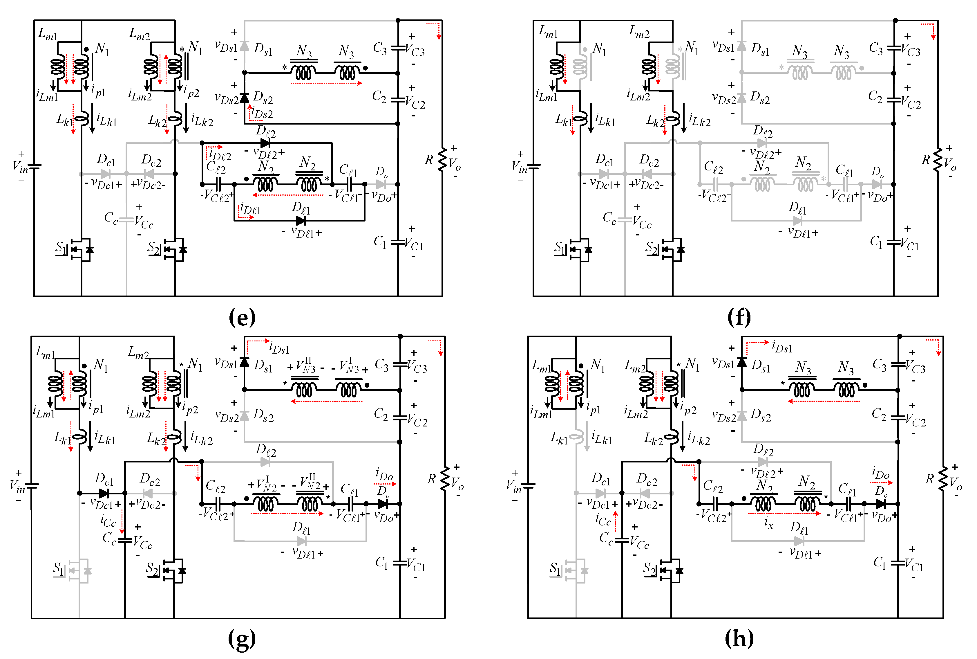
The proposed converter operates in continuous conduction mode (CCM). The gate signals of the power switches are interleaved with 180 ° phase shift, the duty ratios are the same, and they are greater than 0.5. The theoretical waveforms are shown in Figure 3. In CCM operation, the operating mode of the proposed converter can be partitioned into eight stages over one switching period. Figure 4 shows the corresponding circuit models for the eight operating stages.
Stage1 [ t 0 ~ t 1 ]: The equivalent circuit of this stage is depicted in Figure 4a. At t = t 0 , the power switch S 1 starts to turn on with zero-current switching (ZCS) operation, owing to the leakage inductance L k 1 , and S 2 is still in a turn-on state. The diodes D c 1 , D c 2 , D 1 , D 2 and D s 2 are reversed biased, and D o as well as D s 1 are still turned on. The current through L k 1 increases rapidly from zero, while the currents through the secondary and tertiary windings of the coupled inductors decrease. The current falling rates through D o and D s 1 are controlled by the leakage inductances L k 1 and L k 2 , such that the diode reverse recovery problem is alleviated. The stored energy in the magnetizing inductor L m 1 is transferred to the output side via the secondary and tertiary windings of the coupled inductors. The following equations are valid:
i p 2 = i p 1 = n ( i D o + i D s 1 )
i L k 1 = i L m 1 + i p 1 = i L m 1 n ( i D o + i D s 1 )
As the leakage inductor current i L k 1 reaches the magnetizing inductor current i L m 1 , this stage ends. At the same time, the currents through the diodes D o and D s 1 fall to zero, and D o and D s 1 are turned off with ZCS operation.
Stage2 [ t 1 ~ t 2 ]: The power switches S 1 and S 2 remain in a turn-on state, and all of the diodes are in a turn-off state. Figure 4b depicts the corresponding operating circuit. The currents through inductors L m 1 , L k 1 , L m 2 and L k 2 increase linearly because these inductors are charged from the input DC source. The leakage inductor currents are as follows.
i L k 1 ( t ) = i L k 1 ( t 1 ) + V i n L m 1 + L k 1 ( t t 1 )
i L k 2 ( t ) = i L k 2 ( t 1 ) + V i n L m 2 + L k 2 ( t t 1 )
This stage ends when S 2 is turned off.
Stage3 [ t 2 ~ t 3 ]: In this stage, the switch S 2 is in a turn-off state, and S 1 keeps conducting. The operating circuit is illustrated in Figure 4c. The clamp capacitor C c is charged by the current i L k 2 via the clamp diode D c 2 . The leakage inductor energy is released to the capacitor C c . The current i L k 2 decreases linearly. The voltage across the switch S 2 is clamped by the capacitor voltage V C c . The energy stored in L m 2 is released to the capacitors C 1 , C 2 and C 2 via the secondary and tertiary windings of the coupled inductors. The lift capacitors C 1 and C 2 are charged by the lift diode currents i D 1 and i D 2 , respectively. At the same time, the output capacitor C 2 is charged by the current i D s 2 . The following equations are valid:
i p 1 = i p 2 = n i D s 2 + n ( i D 1 + i D 2 )
i L k 2 = i L m 2 n i D s 2 n ( i D 1 + i D 2 )
The stage finishes as i L k 2 falls to zero at t = t 3 , and the clamp diode D c 2 becomes reverse-biased under ZCS operation. Thus, there is no reverse recovery loss for D c 2 .
Stage4 [ t 3 ~ t 4 ]: At the beginning time, the clamp diode D c 2 is naturally turned off when the leakage inductor energy stored in L k 2 has fully released to the clamp capacitor C c . The operating circuit is illustrated in Figure 4d. Magnetizing inductor L m 2 still transfers its energy to charge C 1 , C 2 and C 2 via the secondary and tertiary windings of the coupled inductors. The current through the power switch S 1 is the summation of the currents in the magnetizing inductors L m 1 and L m 2 . The following equations are held in this stage:
i L m 2 = n ( i D 1 + i D 2 ) + n i D s 2
i S 1 = i L m 1 + i L m 2
This stage finishes when the turn-on signal is applied to S 2 .
Stage5 [ t 4 ~ t 5 ]: In this stage, the operating circuit is depicted in Figure 4e. The switch S 2 turns on at time t 4 under ZCS condition, owing to the leakage inductance L k 2 , and S 1 is still conducting. The current i L k 2 increases rapidly from zero, and the currents in the secondary and tertiary windings of the coupled inductors decrease. The current falling rates through D 1 , D 2 and D s 2 are dominated by L k 1 and L k 2 , such that the diode reverse recovery problem is mitigated. As the leakage inductor current i L k 2 reaches i L m 2 , this stage ends at t = t 5 . At the same time, the currents through D 1 , D 2 and D s 2 fall to zero, and these diodes are naturally turned off with ZCS operation.
Stage6 [ t 5 ~ t 6 ]: The switches S 1 and S 2 are conducting in this interval. All of the diodes are in a turn-off state. The operating circuit is depicted in Figure 4f. The operating modes of stages 1 and 6 are similar. At the end of this stage the switch S 1 is turned off.
Stage7 [ t 6 ~ t 7 ]: The switch S 1 is turned off at time t 6 . The operating circuit is illustrated in Figure 4g. One part of the leakage inductor energy stored in L k 1 is released to the clamped capacitor C c , and another part of the leakage inductor energy is recycled to the output side. The leakage inductor current i L k 1 is falling. The input voltage V i n , C 2 and C 1 are in series connection to transfer energy to the output capacitor C 1 via diodes D c 1 and D o , as well as the primary and secondary windings of the coupled inductors, thus extending the voltage on the output capacitor C 1 . The stored energy in L m 1 is delivered to the secondary and tertiary windings of the coupled inductors, such that output capacitor C 3 is charged by the diode current i D s 1 , and C 1 is charged by the diode current i D o . As the leakage inductor current i L k 1 drops to zero, the diode D c 1 becomes reverse-biased and turns off at time t 7 under ZCS condition. Thus, there is no reverse recovery loss for D c 1 . At this moment, this stage ends.
Stage 8 [ t 7 ~ t 8 ]: Figure 4h illustrates the operating circuit. At the beginning time, the leakage inductor energy stored in L k 1 has completely released. Magnetizing inductor L m 1 still transfers energy to the capacitors C 1 and C 3 via the secondary and tertiary windings of the coupled inductors. The capacitors C c , C 1 , C 2 and the secondary windings are connected in series to transfer their energy to the output capacitor C 1 . The current in the switch S 2 is the summation of the currents i L m 1 and i L m 2 . The switch S 1 is turned on at the end of this stage. Then, a new switching period begins to start.

3. Steady-State Analysis

3.1. Voltage Gain Derivation

To briefly describe the voltage gain derivation, the following assumptions are used:
(1)
All of the semiconductors are regarded as ideal. The on-state resistance of the switches and the forward voltage drop of the diodes are ignored.
(2)
The leakage inductances are neglected.
(3)
The magnetizing inductances of the coupled inductors are regarded as the same; that is, L m 1 = L m 2 = L m .
All of the capacitors are large enough. As a result, the voltages across them are considered constant during one switching period. Based on the volt-second balance principle of the magnetizing inductance L m 1 , the voltage on the clamp capacitor C c can be derived as
V C c = 1 1 D V i n
where D is the operating duty ratio. The result in Equation (9) is identical to the output voltage of a conventional boost converter.
Let the voltages across the secondary and tertiary windings of the coupled inductors be denoted by V N 2 I and V N 3 I , V N 2 II and V N 3 II , respectively. According to Kirchhoff’s Voltage Low (KVL), the voltages across the lift capacitors C 1 and C 2 can be calculated from stage 3 as
V C 1 = V C 2 = V N 2 I V N 2 II = n V i n n ( V i n V C c ) = n V C c
Moreover, it also yields
V C 2 = V N 3 I V N 3 II = n V i n n ( V i n V C c ) = n V C c
Substituting Equation (9) into Equations (10) and (11), the capacitor voltages are rewritten as
V C 1 = V C 2 = n 1 D V i n
V C 2 = n 1 D V i n
By applying KVL in stage 7, the voltage V C 3 across the output capacitor C 3 can be derived as
V C 3 = V N 3 II V N 3 I = n V C c = n 1 D V i n
Moreover, the voltage across the output capacitor C 1 is derived as
V C 1 = V N 2 II V N 2 I + V C c + V C 1 + V C 2 = 3 n + 1 1 D V i n  
According to (13)–(15), the output voltage can be obtained as follows:
V o = V C 1 + V C 2 + V C 3 = 5 n + 1 1 D V i n
Hence, we have the ideal voltage gain M of the proposed converter as
M = V o V i n = 5 n + 1 1 D
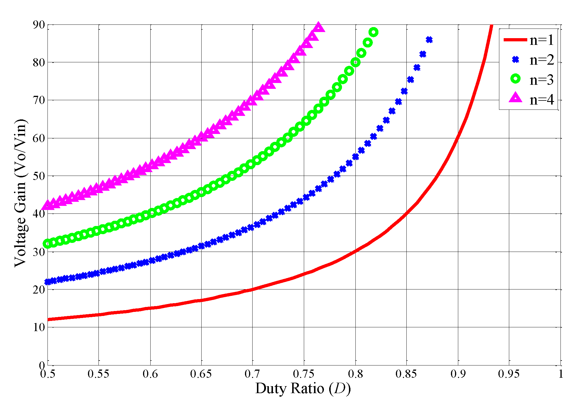
The plot of voltage gain M versus turns ratio n and duty ratio D is drawn in Figure 5. It shows that the turns ratio has a significant impact on the step-up voltage gain. In addition, the high voltage gain can be achieved without any extreme duty ratio or high turns ratio in the proposed converter. When the duty ratio is merely 0.6 and turns ratio n = 1 , the voltage gain is calculated as 15.

3.2. Voltage Stresses on Semiconductor Devices

The steady-state analysis reveals that the voltage on the power switches and the clamp diodes during their off-state are all equal to the voltage on the clamp capacitor. From Equations (9) and (17), the voltage stresses are given by
V S 1 = V S 2 = V D c 1 = V D c 2 = V C c = 1 1 D V i n = 1 5 n + 1 V o
Moreover, the voltage stress on the switching diode D s 1 can be derived as
V D s 1 = V C 2 + V C 3 = 2 n 1 D V i n = 2 n 5 n + 1 V o
The voltage stress on the output diode D o is given by
V D o = V C 1 V C 1 V C c = 2 n 1 D V i n = 2 n 5 n + 1 V o
Similarly, the voltage stresses on the diodes D s 2 , D 1 and D 2 can be derived as
V D s 2 = V D 1 = V D 2 = 2 n 1 D V i n = 2 n 5 n + 1 V o
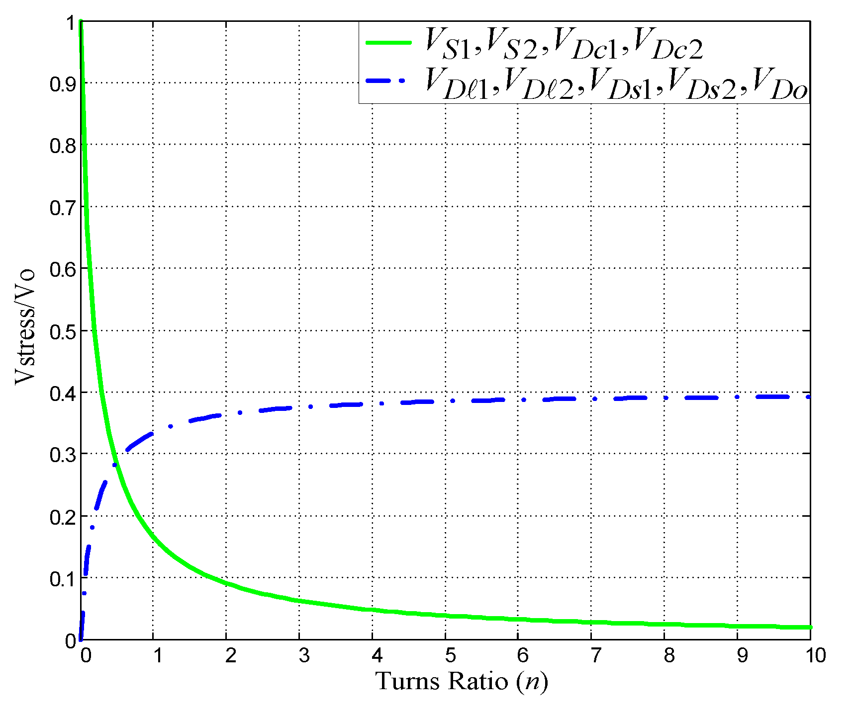
From Equations (18)–(21), the relationship between the normalized voltage stresses on semiconductor devices and the turns ratio of the coupled inductors is shown in Figure 6.
As the turns ratio increases, the voltage stresses on S 1 , S 2 , D c 1 and D c 2 decrease, and the voltage stresses on the other diodes become large. It is worth noting that the voltage stresses are lower than the output voltage. As a result, power MOSFETs with low R d s ( ON ) and diodes with low forward voltage drop can be employed to reduce the on-state losses and improve the conversion efficiency.

3.3. Design Considerations

3.3.1. Design of Coupled Inductors

The turns ratio of the coupled inductors is designed from Equation (17). Once the duty ratio has been selected, the turns ratio n can be properly designed by
n = N 3 N 1 = N 2 N 1 = ( 1 D ) V o 5 V i n 1 5
Once the turns ratio of the coupled inductor is obtained, the magnetizing inductance can be determined from the CCM operation mode and an acceptable current ripple. The current ripple on the magnetizing inductor is identical, and given by
Δ i L m = V i n D L m f s
where f s is the switching frequency. The average magnetizing current can be derived as
I L m = P o 2 V i n = V o 2 2 V i n R
where Po is the output power. For CCM operation, the following condition holds:
I L m 1 2 Δ i L m > 0
Substituting Equations (23) and (24) into (25), the condition of magnetizing inductance for CCM operation is expressed as
L m > V i n 2 D P o f s = D ( 1 D ) 2 V o 2 ( 5 n + 1 ) 2 P o f s = D ( 1 D ) 2 R ( 5 n + 1 ) 2 f s

3.3.2. Design of Capacitors

The capacitors are determined to limit their voltage ripples to within an acceptable range. The output capacitor C 1 is discharged by the average load current I o from Stage 2 to Stage 6. Thus, its voltage ripple can be derived as
Δ V C 1 = D I o C 1 f s
Substituting Equations (15) and (17) into (27), the required capacitance is calculated as
C 1 = ( 5 n + 1 ) D ( 3 n + 1 ) R f s ( Δ V C 1 / V C 1 )
which is expressed by the specified voltage ripple on the output capacitor C 1 . Similarly, one can obtain the design of the following capacitors in terms of their own specified voltage ripples:
C 2 = C 3 = ( 5 n + 1 ) D n R f s ( Δ V C i / V C i ) ,   i = 2 ,   3
C c = 5 n + 1 R f s ( Δ V C c / V C c )

3.4. Performance Comparison

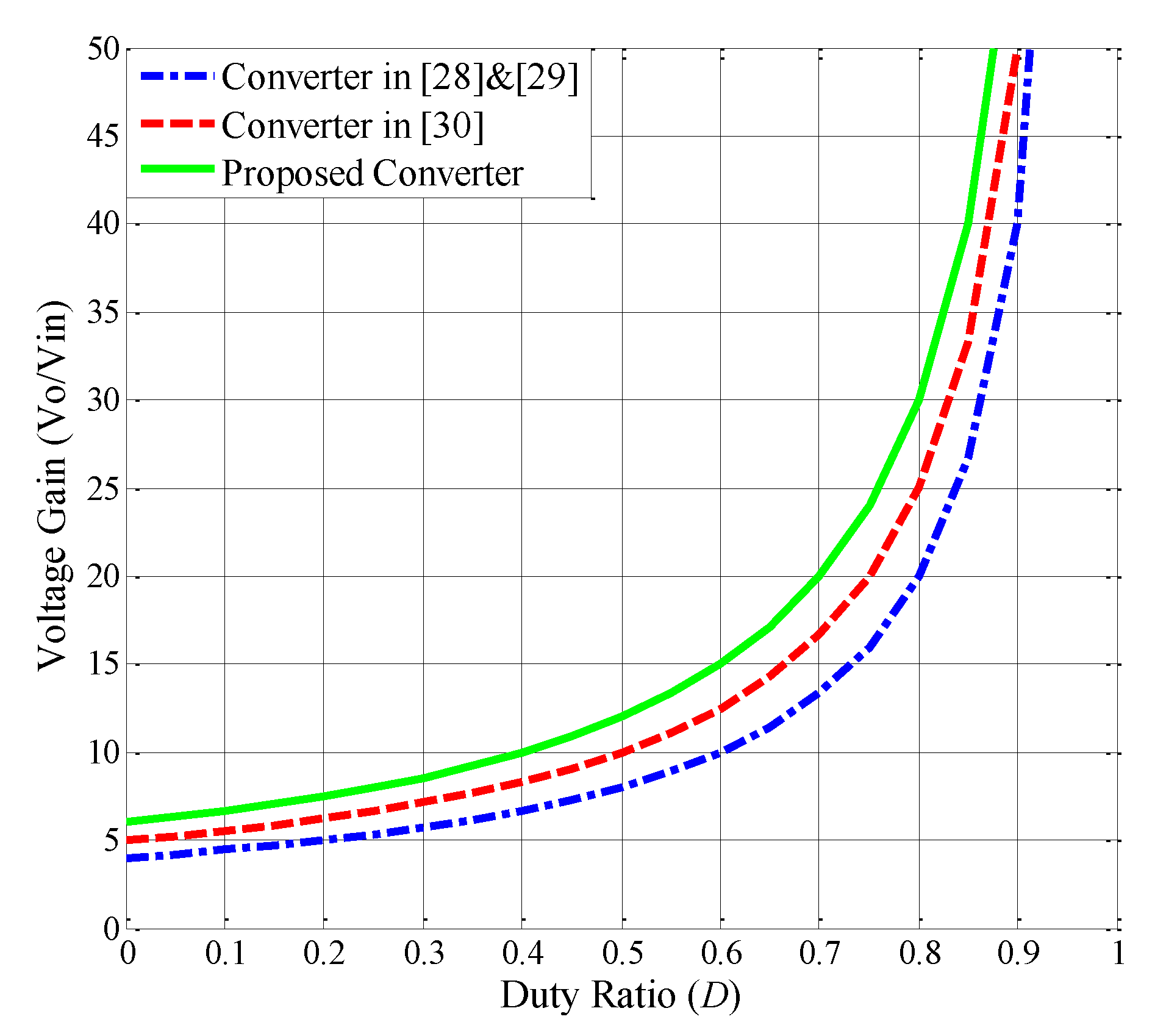
Table 1 shows the performance comparison between the proposed converter and some interleaved high step-up converters published in [28,29,30], including voltage gain, voltage stress on switches, maximum diode voltage stress and the quantities of the devices. In these comparative converters, three-winding coupled inductors are employed to achieve high step-up voltage gain. Figure 7 shows the voltage gain comparison with turns ratio n = 1. As can be seen, the proposed converter has the highest voltage gain. In addition, it also has the lowest voltage stresses on the switches and diodes. The voltage stresses on the semiconductor devices are lower than the high output voltage, which results in the use of switches with low on-resistance and diodes with low forward voltage drop to reduce the conduction losses and improve the conversion efficiency. As a result, it is clear that the proposed converter is very suitable for applications requiring high efficiency and a high step-up voltage conversion ratio.
C 1 = C 2 = 5 n + 1 n R f s ( Δ V C j / V C j ) , j = 1 , 2

4. Controller Design

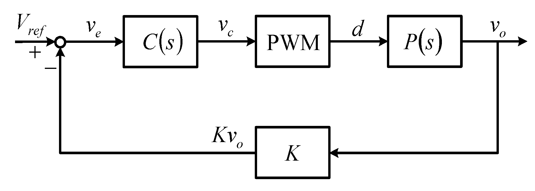
For the purposes of the output voltage regulation, regardless of the variations of input voltage and output load, the voltage-mode feedback control system was built as shown in Figure 8. Blocks C(s) and PWM represent the controller and pulse-width modulator, respectively. Block P(s) denotes the converter power stage. Block K denotes the sensor gain.
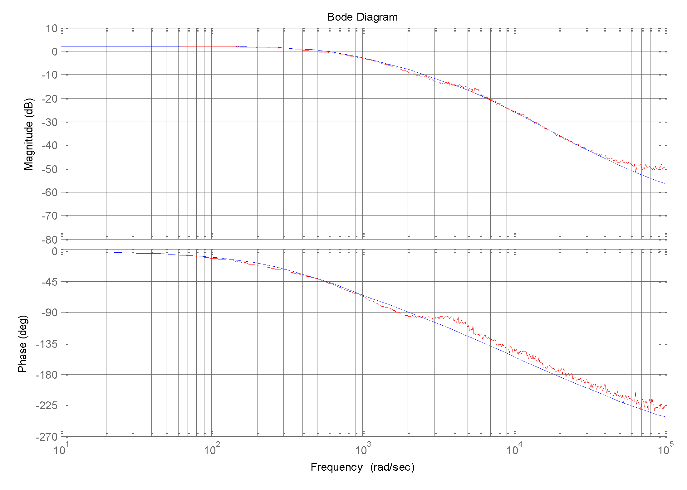
A small-signal model was investigated through the frequency response with experimental measurements for the prototype converter. The electrical specifications and component parameters of the prototype converter are shown in Table 2. The experimental frequency response at the operating point of half load was measured by an NF FRA5012 frequency response analyzer. The Bode plot of the measured transfer function from control to scaled output voltage ( v ˜ c to K v ˜ o ) is shown in Figure 9 with red curves. The corresponding transfer function can be obtained by the curve-fitting method, and it is given by
G ( s ) = K v ˜ o ( s ) v ˜ c ( s ) = 138.3 ( s 45000 ) ( s + 700 ) ( s + 7000 )
The Bode plot of the curve-fitting transfer function in Equation (32), together with the measured results, is shown in Figure 9. Comparing the magnitude and phase curves, it can be seen that the curves agree well with each other. Thus, the curve-fitting transfer function expressed in Equation (32) can be used for the controller design.
Based on the K-factor method [31], a type III controller [32] with three-pole and two-zero was designed for the closed-loop control system. One of the poles of the controller was located at the origin to achieve the zero steady-state error, while the other two poles were positioned below the desired crossover frequency to attenuate the switching noises in the feedback loop. In addition, the zeros and gain of the controller were adjusted to achieve the desired phase margin at the crossover frequency. The controller transfer function was designed as
C ( s ) = 3 . 3 × 10 6 ( s + 2659 ) ( s + 2673 ) s ( s + 1 . 49 × 10 4 ) 2
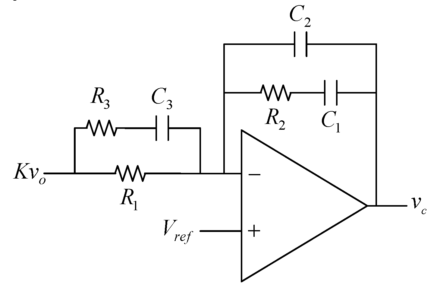
The controller was implemented by the operational amplifier circuit, as shown in Figure 10, and its transfer function is given by
v ˜ c ( s ) K v ˜ o ( s ) = R 1 + R 3 R 1 R 3 C 2 ( s + 1 R 2 C 1 ) ( s + 1 ( R 1 + R 3 ) C 3 ) s ( s + 1 R 2 C 1 C 2 / ( C 1 + C 2 ) ) ( s + 1 R 3 C 3 )
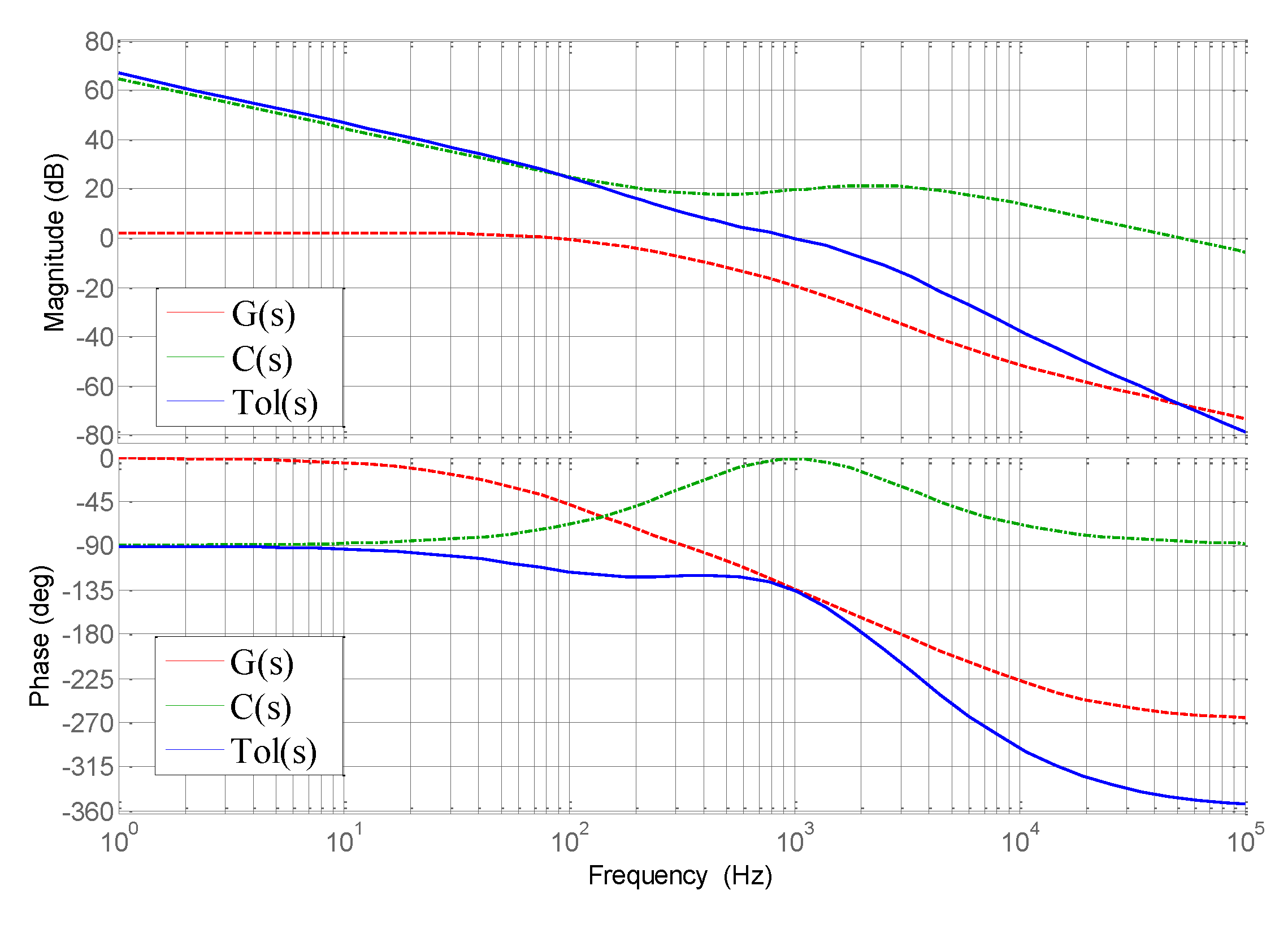
The Bode plots of the plant G(s), the controller C(s) and the loop gain Tol(s) = G(s)C(s) are shown in Figure 11. As a result, a crossover frequency of 1 kHz and a phase margin of 45° were achieved for the output voltage controlled system.

5. Experimental Verification

An experimental prototype with maximal output power 1 kW was implemented and tested to verify the performance of the proposed converter. Table 2 shows the components and parameters of the prototype converter [33]. Figure 12, Figure 13, Figure 14, Figure 15 and Figure 16 show the simulated results using IsSpice software and the experimental results under full load 1 kW condition, as described below.
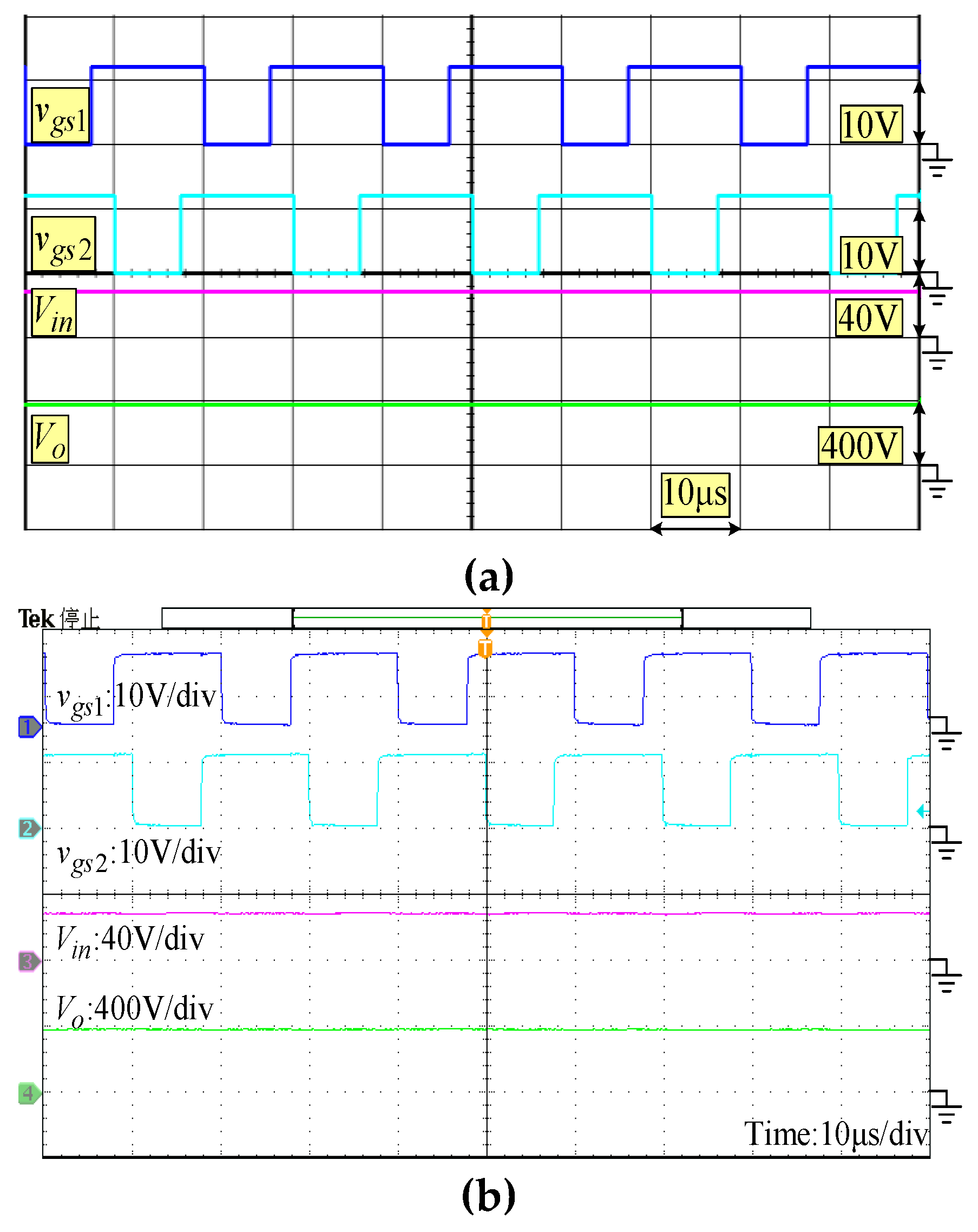
Figure 12 shows the waveforms of V i n , V o , and the gate signals v g s 1 and v g s 2 , for the switches S 1 and S 2 with interleaved operation. It can be seen that the high voltage gain was over 13 times; however, the duty ratios of the switches were not extremely large.
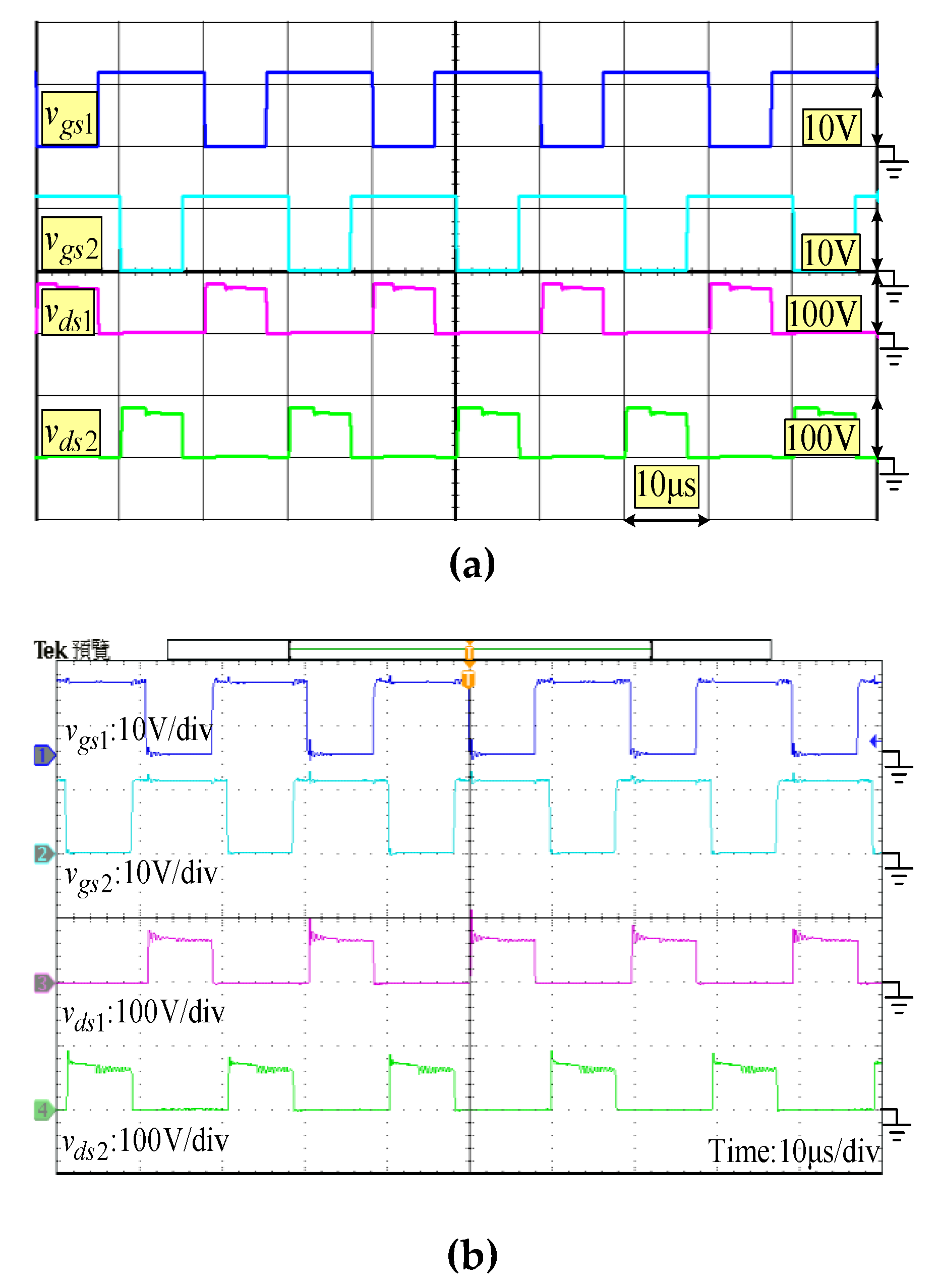
Figure 13 illustrates the gate signals and the drain-source voltage waveforms v d s 1 and v d s 2 for the switches S 1 and S 2 . It was observed that the voltage stress on S 1 and S 2 was only about 63 V, which is V o / 6 . The switch voltage stress was much lower than the output voltage. This result meets with that of the steady-state analysis in Equation (18). Therefore, the power switch with a low voltage rating and low on-resistance can be chosen to reduce the conduction losses.
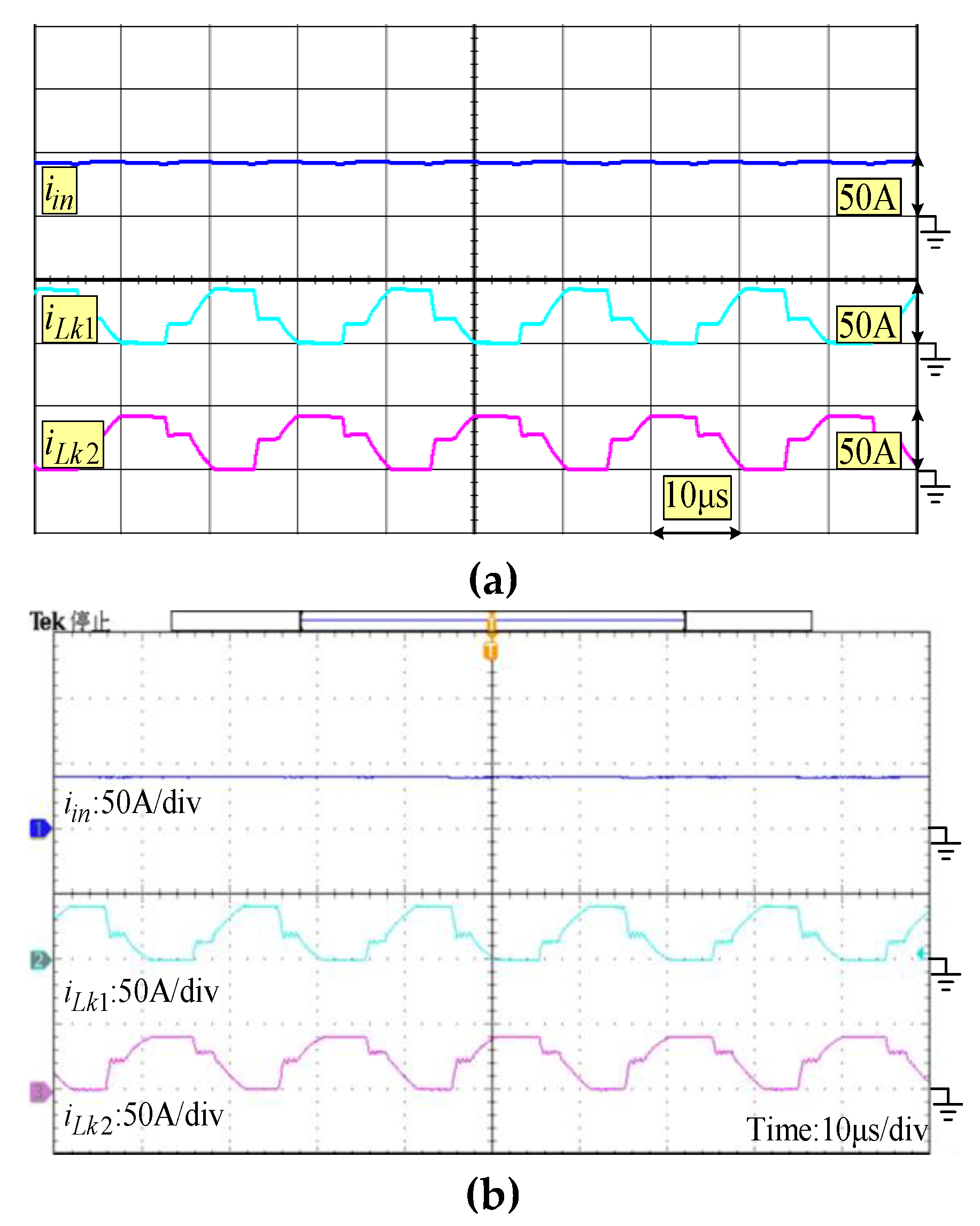
Figure 14 represents the input current i i n and the leakage inductor currents i L k 1 and i L k 2 . Since the input current i i n is equal to i L k 1 plus i L k 2 , one can see that the interleaved operation helps the ripple current cancellation. Consequently, the input current ripple is really small. The ripple current reduction is helpful for the lifetime of green energy sources. Moreover, a good input current sharing capability can be observed by the leakage inductor currents for the two phases of the proposed converter.
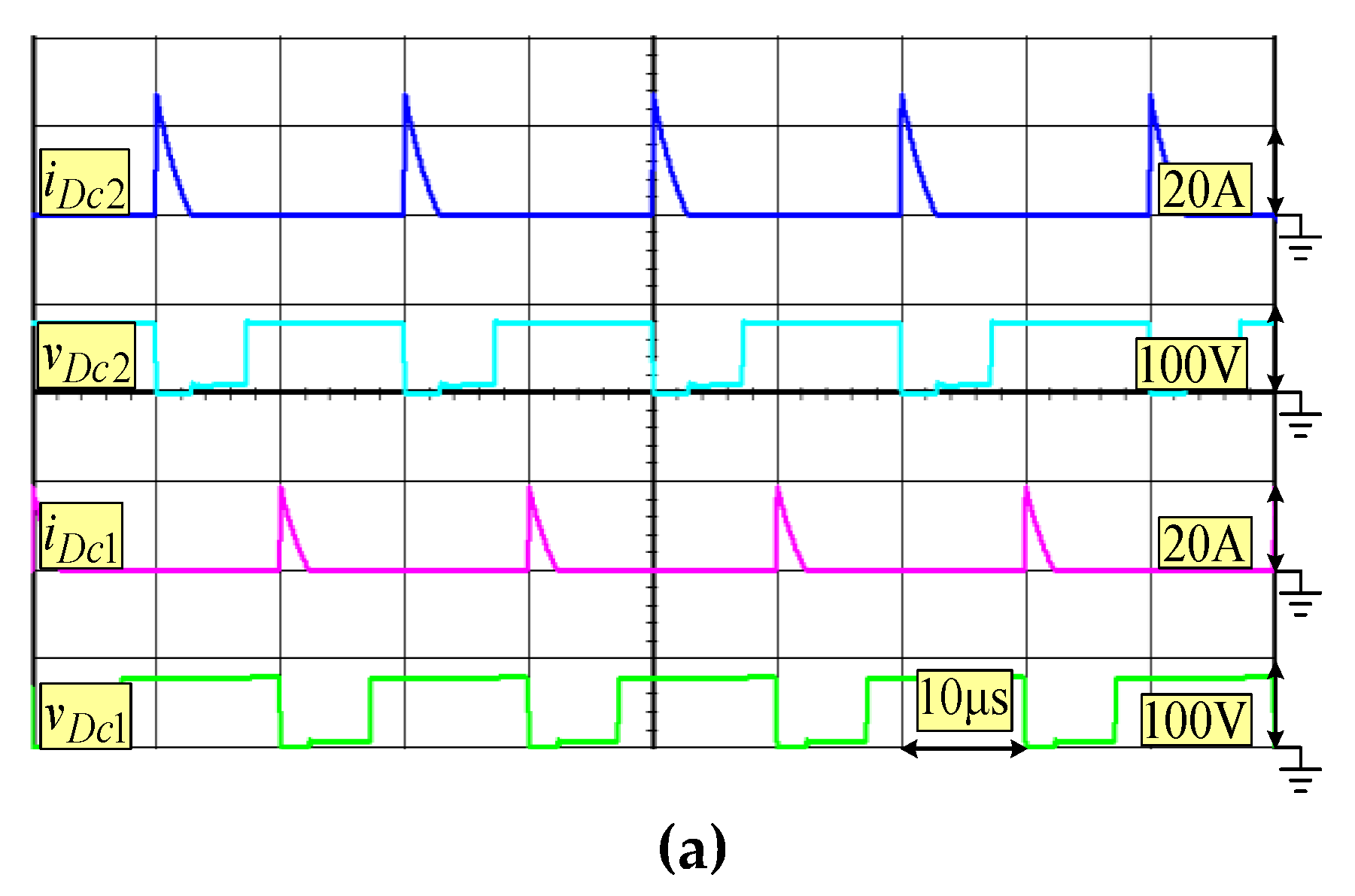
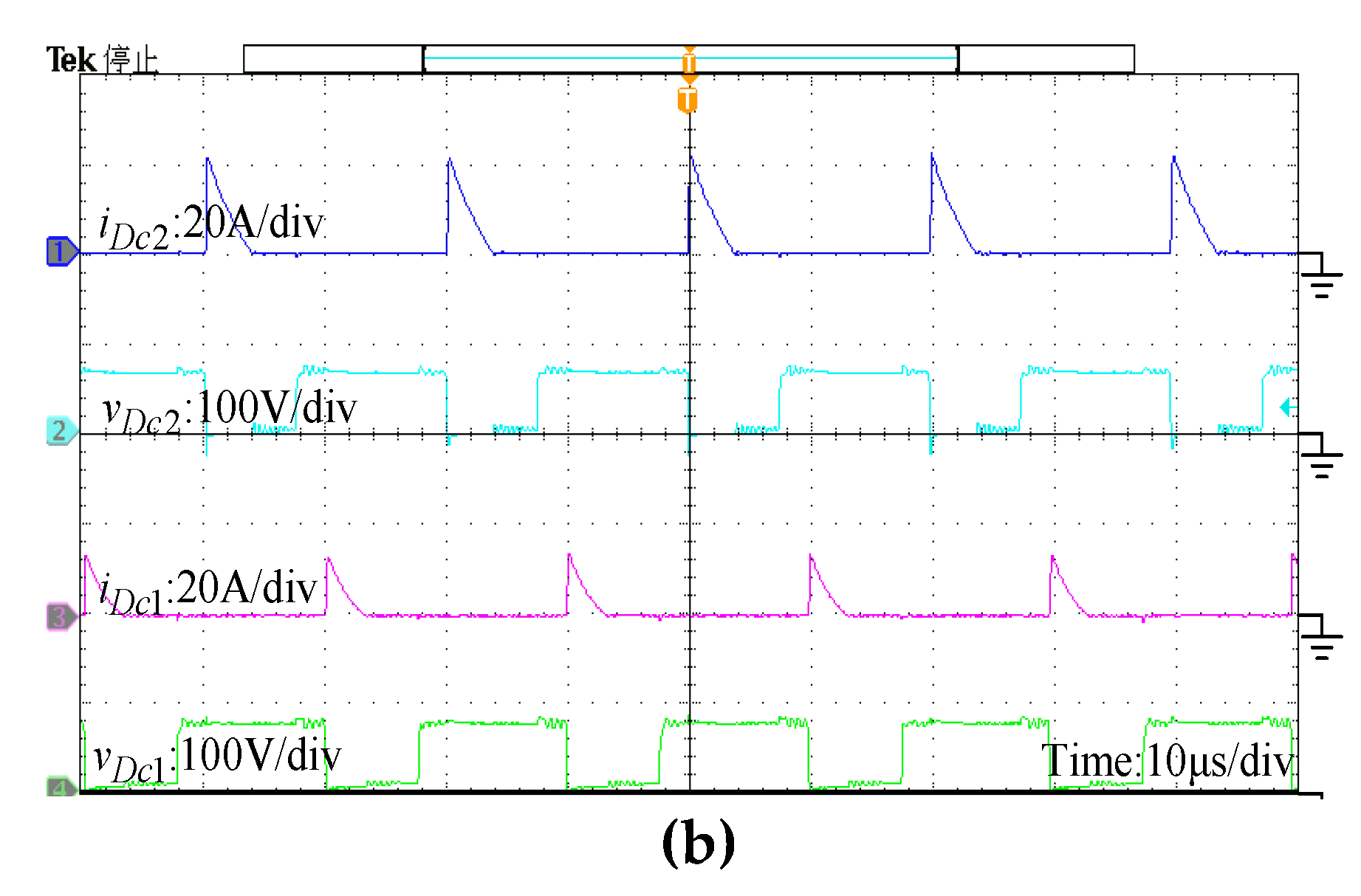
Figure 15 exhibits the currents and voltage waveforms on the clamped diodes D c 1 and D c 2 . One can see that the voltage stress on the diodes is about 63 V, which is only one-sixth of the output voltage. The experimental results show good agreement with the theoretical result in (18). In addition, as can be seen, the currents i D c 1 and i D c 2 fell to zero, and then the considered diodes turned off with the ZCS operation, which is consistent with the operating analysis in stages 3 and 7. Thus, there are no reverse-recovery losses for the clamped diodes D c 1 and D c 2 .
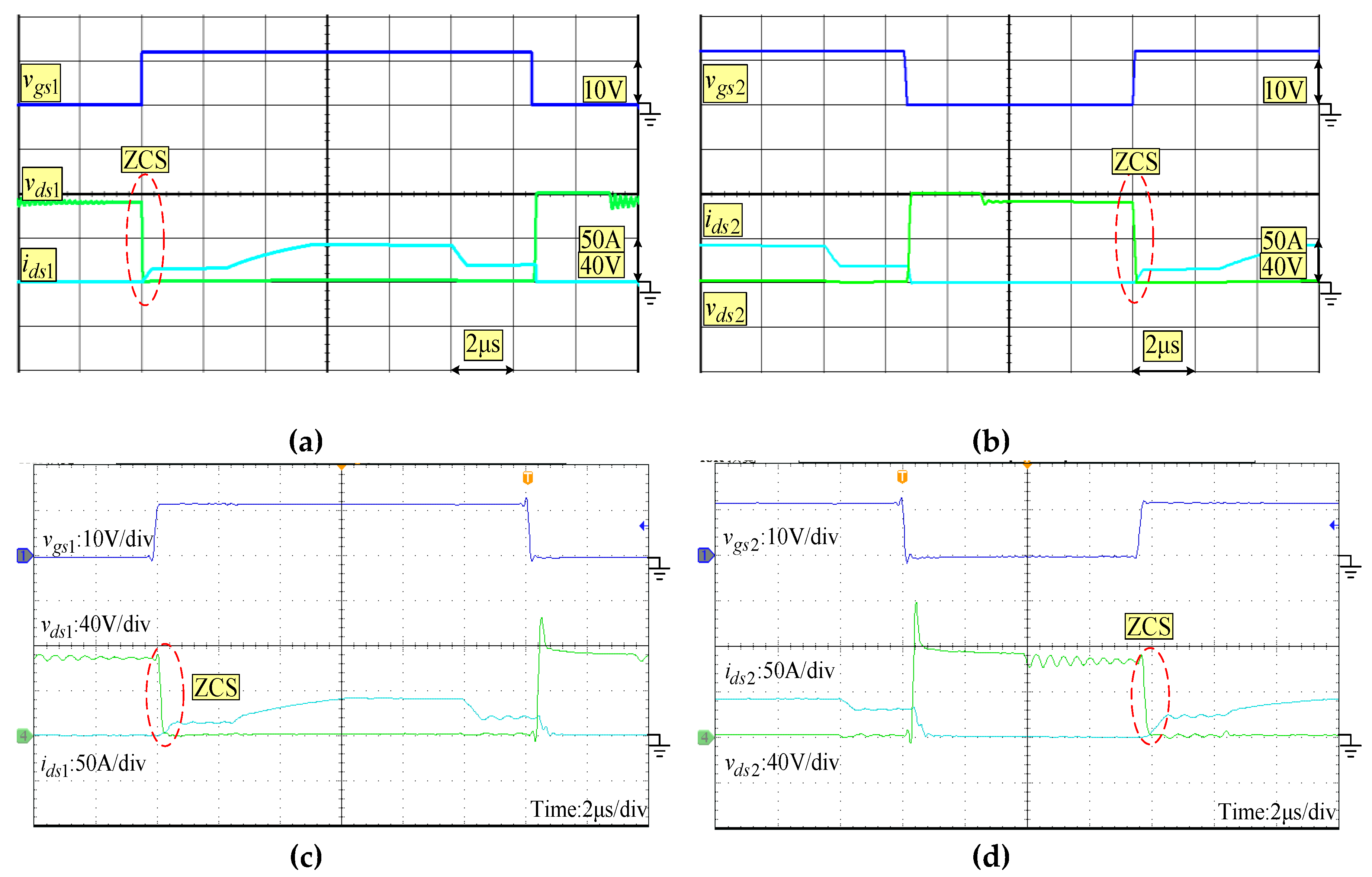
In Figure 16, the simulated and experimental waveforms of the voltages and the currents on the switches S 1 and S 2 are illustrated. It can be seen that the power switches can achieve ZCS turn-on operation. The switching losses are reduced accordingly for high efficiency.
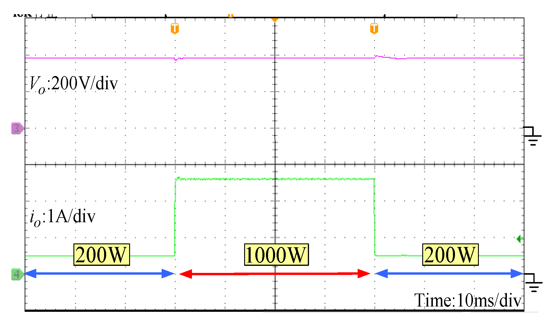
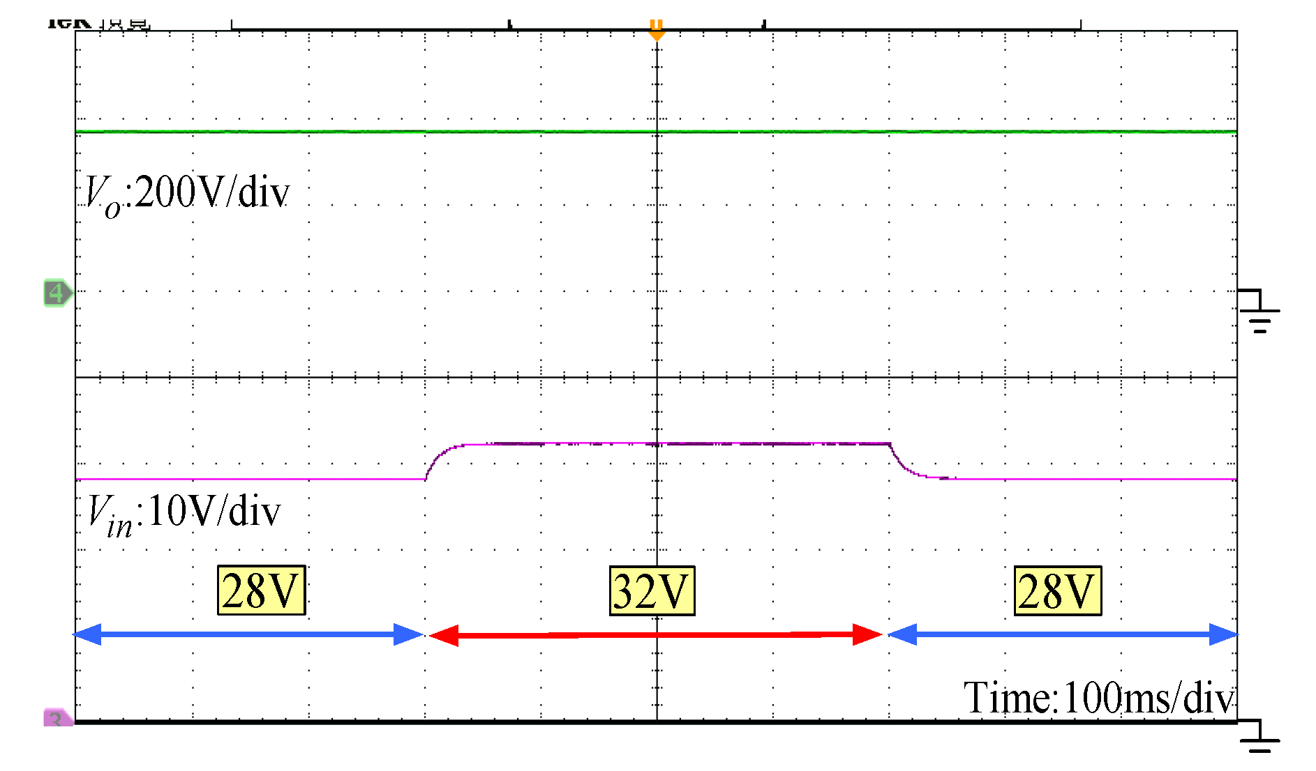
Figure 17 shows the dynamic response of the output voltage under the load variation between 200W and 1000W using a dc electronic load. The dynamic response of the output voltage under the input voltage varying from 28 V to 32 V, and vice versa, is shown in Figure 18. As shown in the figures, the output voltage is insensitive to the load change and input voltage variation. It means that the well dynamic performance of the output voltage regulation can be provided with the closed-loop controller design.
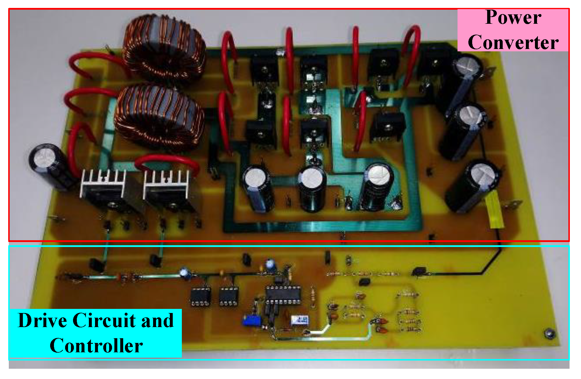
Figure 19 represents the conversion efficiency of the prototype converter under various output powers. A high precision power analyzer (HIOKI 3390) was employed to measure the power conversion efficiency, which is the ratio of the measured output power over the measured input power, Pout/Pin. The measured maximum conversion efficiency was up to 98%, which was obtained at the output power of 100 W. Moreover, the conversion efficiency was 91.08% at the full-load condition. At higher output power, the on-state conduction losses of switching devices are high. Then, the efficiency decreases. The photograph of the laboratory prototype is illustrated in Figure 20.

6. Conclusions

The three-winding coupled inductors and voltage multiplier cells, and the voltage-lift and voltage-stack techniques were utilized to create a novel high step-up DC–DC converter configuration, which is suitable for applications in PV generation systems. The proposed high step-up converter gets high voltage gain conversion with proper duty ratio operation and low voltage stresses on the switches and diodes. Switches with smaller on-resistance and diodes with lower forward voltage drop can thereby be used to reduce the conduction losses. The interleaved operation reduces the input current ripple. Moreover, the diode reverse-recovery loss is alleviated due to the leakage inductances of the coupled inductors. The leakage inductor energy is absorbed and recycled to improve efficiency. This paper presented the operating principle and steady-state analysis of the proposed converter. The closed-loop controller is also well designed for the output voltage regulation, regardless of the variations in the input voltage or output load. Finally, a 1 kW laboratory prototype was tested to verify the performance and the presented analysis. The experimental results showed that the proposed converter is suitable for high efficiency and high voltage gain in DC–DC conversion.

Author Contributions

S.-J.C. and S.-P.Y.: analysis and design. Y.-H.C.: experiment. C.-M.H.: supervision and inspection. S.-J.C. and S.-P.Y.: writing and editing. All authors have read and agreed to the published version of the manuscript.

Funding

This work was financially supported by the Green Energy Technology Research Center from The Featured Areas Research Center Program within the framework of the Higher Education Sprout Project by the Ministry of Education (MOE) in Taiwan, and the Ministry of Science and Technology, Taiwan, under grant numbers MOST 108-2221-E-168-004.

Conflicts of Interest

The authors declare that there is no conflict of interest.

References

  1. Ajami, A.; Ardi, H.; Farakhor, A. A novel high step-up DC-DC converter based on integrating coupled inductor and switched-capacitor techniques for renewable energy applications. IEEE Trans. Power Electron. 2015, 30, 4255–4263. [Google Scholar] [CrossRef]
  2. Yang, B.; Li, W.; Zhao, Y.; He, X. Design and analysis of a grid connected PV power system. IEEE Trans. Power Electron. 2010, 25, 992–1000. [Google Scholar] [CrossRef]
  3. Carrasco, J.M.; Franquelo, L.G.; Bialasiewicz, J.T.; Galvan, E.; PortilloGuisado, R.C.; Prats, M.A.M.; Leon, J.I.; Moreno-Alfonso, N. Power-electronic systems for the grid integration of renewable energy sources: A survey. IEEE Trans. Ind. Electron. 2006, 53, 1002–1016. [Google Scholar] [CrossRef]
  4. Andrade, A.M.; Schuch, L.; Martins, M.L.S. Analysis and design of high-efficiency hybrid high step-up DC–DC converter for distributed PV generation systems. IEEE Trans. Ind. Electron. 2019, 66, 3860–3868. [Google Scholar] [CrossRef]
  5. Tofoli, F.L.; Pereira, D.C.; Paula, W.J.; Junior, D.S.O. Survey on non-isolated high-voltage step-up DC–DC topologies based on the boost converter. IET Power Electron. 2015, 8, 2044–2057. [Google Scholar] [CrossRef] [Green Version]
  6. Wong, Y.S.; Chen, J.F.; Liu, K.B.; Hsieh, Y.P. A novel high step-up DC-DC converter with coupled inductor and switched clamp capacitor techniques for photovoltaic systems. Energies 2017, 10, 378–394. [Google Scholar] [CrossRef] [Green Version]
  7. Hu, X.; Gong, C. A high voltage gain DC-DC converter integrating coupled-inductor and diode-capacitor techniques. IEEE Trans. Power Electron. 2014, 29, 789–800. [Google Scholar]
  8. Farakhor, A.; Abapour, M.; Sabahi, M.; Farkoush, S.G.; Oh, S.R.; Rhee, S.B. A study on an improved three-winding coupled inductor based dc/dc boost converter with continuous input current. Energies 2020, 13, 1780. [Google Scholar] [CrossRef] [Green Version]
  9. Tseng, K.C.; Lin, J.T.; Huang, C.C. High step-up converter with three-winding coupled inductor for fuel cell energy source applications. IEEE Trans. Power Electron. 2015, 30, 574–581. [Google Scholar] [CrossRef]
  10. Yu, D.; Yang, J.; Xu, R.; Xia, Z.; Iu, H.H.; Fernando, T. A family of module-integrated high step-up converters with dual coupled inductors. IEEE Access 2018, 6, 16256–16266. [Google Scholar] [CrossRef]
  11. Azizkandi, M.E.; Sedaghati, F.; Shayeghi, H.; Blaabjerg, F. Two- and three-winding coupled-inductor-based high step-up DC–DC converters for sustainable energy applications. IET Power Electron. 2020, 13, 144–156. [Google Scholar]
  12. Gao, Y.; Liu, H.; Ai, J. Novel high step-up DC–DC converter with three-winding-coupled-inductors and its derivatives for a distributed generation system. Energies 2018, 11, 3428. [Google Scholar] [CrossRef] [Green Version]
  13. Azizkandi, M.E.; Sedaghati, F.; Shayeghi, H.; Blaabjerg, F. A high voltage gain DC–DC converter based on three winding coupled inductor and voltage multiplier cell. IEEE Tran. Power Electron. 2020, 35, 4558–4567. [Google Scholar] [CrossRef]
  14. Wei, C.L.; Shih, M.H. Design of a switched-capacitor DC-DC converter with a wide input voltage range. IEEE Trans. Circuits Syst. 2013, 60, 1648–1656. [Google Scholar] [CrossRef]
  15. Tang, Y.; Fu, D.; Wang, T.; Xu, Z. Hybrid switched-inductor converters for high step-up conversion. IEEE Trans. Ind. Electron. 2015, 62, 1480–1490. [Google Scholar] [CrossRef]
  16. Axelrod, B.; Berkovich, Y.; Ioinovici, A. Switched-capacitor/switched-inductor structures for getting transformerless hybrid DC–DC PWM converters. IEEE Trans. Circuits Syst. 2008, 55, 687–696. [Google Scholar] [CrossRef]
  17. Salvador, M.A.; Lazzarin, T.B.; Coelho, R.F. High step-up DC-DC converter with active switched-inductor and passive switched-capacitor networks. IEEE Trans. Ind. Electron. 2018, 65, 5644–5654. [Google Scholar] [CrossRef]
  18. Gu, Y.; Chen, Y.; Zhang, B.; Qiu, D.; Xie, F. High step-up DC–DC converter with active switched LC-network for photovoltaic systems. IEEE Trans. Energy Convers. 2019, 34, 321–329. [Google Scholar] [CrossRef]
  19. Duong, T.D.; Nguyen, M.K.; Tran, T.T.; Lim, Y.C.; Choi, J.H. Transformerless high step-up DC-DC converters with switched-capacitor network. Electronics 2019, 8, 1420. [Google Scholar] [CrossRef] [Green Version]
  20. Lakshmi, M.; Hemamalini, S. Nonisolated high gain DC-DC converter for DC microgrids. IEEE Trans. Ind. Electron. 2018, 65, 1205–1212. [Google Scholar] [CrossRef]
  21. Bhaskar, M.S.; Meraj, M.; Iqbal, A.; Padamanaban, S.; Maroti, P.K.; Alammari, R. High gain transformer-less double-duty-triple-mode DC/DC converter for DC microgrid. IEEE Access 2019, 7, 36353–36370. [Google Scholar] [CrossRef]
  22. Tseng, K.C.; Chen, C.T.; Cheng, C.A. A high-efficiency high step-up interleaved converter with a voltage multiplier for electric vehicle power management applications. J. Power Electron. 2016, 16, 414–424. [Google Scholar] [CrossRef] [Green Version]
  23. Zhou, W.B.; Zhu, X.; Luo, Q.M.; Chen, S. Interleaved non-isolated high step-up dc/dc converter based on the diode-capacitor multiplier. IET Power Electron. 2014, 7, 390–397. [Google Scholar] [CrossRef]
  24. Li, W.; Zhao, Y.; Deng, Y.; He, X. Interleaved converter with voltage multiplier cell for high step-up and high-efficiency conversion. IEEE Trans. Power Electron. 2010, 25, 2397–2408. [Google Scholar] [CrossRef]
  25. Li, W.; Xiang, X.; Li, C.; Li, W.; He, X. Interleaved high step-up ZVT converter with built-in transformer voltage doubler cell for distributed PV generation system. IEEE Trans. Power Electron. 2013, 28, 300–313. [Google Scholar] [CrossRef]
  26. Li, W.; Xiang, X.; Hu, Y.; He, X. High step-up interleaved converter with built-in transformer voltage multiplier cells for sustainable energy applications. IEEE Trans. Power Electron. 2014, 29, 2829–2836. [Google Scholar] [CrossRef]
  27. Nouri, T.; Vosoughi, N.; Hosseini, S.H.; Babaei, E.; Sabahi, M. An interleaved high step-up converter with coupled inductor and built-in transformer voltage multiplier cell techniques. IEEE Trans. Ind. Electron. 2019, 66, 1894–1905. [Google Scholar] [CrossRef]
  28. Li, W.; Zhao, Y.; Wu, J.; He, X. Interleaved high step-up converter with winding-cross-coupled inductors and voltage multiplier cells. IEEE Trans. Power Electron. 2012, 27, 133–143. [Google Scholar] [CrossRef]
  29. He, L.; Liao, Y. An advanced current-autobalance high step-up converter with a multicoupled inductor and voltage multiplier for a renewable power generation system. IEEE Trans. Power Electron. 2016, 31, 6992–7005. [Google Scholar]
  30. Nouri, T.; Hosseini, S.H.; Babaei, E.; Ebrahimi, J. Interleaved high step-up DC–DC converter based on three-winding high-frequency coupled inductor and voltage multiplier cell. IET Power Electron. 2015, 8, 175–189. [Google Scholar] [CrossRef]
  31. Venable, D. The K factor: A new mathematical tool for stability analysis and synthesis. Proc. Powercon 1983, 10. Available online: http://citeseerx.ist.psu.edu/viewdoc/download?doi=10.1.1.196.6850&rep=rep1&type=pdf (accessed on 10 May 2020).
  32. Cao, L. Type III compensator design for power converters. Power Electron. Technol. 2011, 1, 20–25. [Google Scholar]
  33. Chen, S.J.; Yang, S.P.; Huang, C.M.; Chen, Y.H. High step-up interleaved converter with three-winding coupled inductors and voltage multiplier cells. In Proceedings of the 20th IEEE International Conference on Industrial Technology (ICIT), Melbourne, VIC, Australia, 13–15 February 2019; pp. 458–463. [Google Scholar]
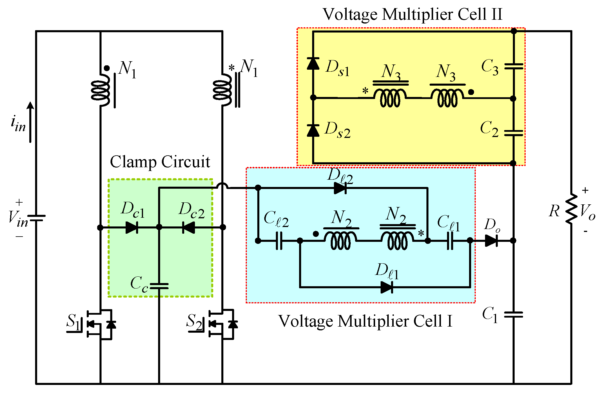
Figure 1. Circuit configuration of the proposed converter.
Energies 13 02537 g001
Figure 2. Equivalent circuit of the proposed converter.
Energies 13 02537 g002
Figure 3. Theoretical waveforms of the proposed converter.
Energies 13 02537 g003
Figure 4. Operating stages of the proposed converter. (a) Stage 1, (b) Stage 2, (c) Stage 3, (d) Stage 4, (e) Stage 5, (f) Stage 6, (g) Stage 7, (h) Stage 8.
Energies 13 02537 g004aEnergies 13 02537 g004b
Figure 5. Voltage gain curve versus duty ratio with different turns ratio.
Energies 13 02537 g005
Figure 6. Normalized voltage stresses on semiconductor devices.
Energies 13 02537 g006
Figure 7. Voltage gain comparison with turns ratio n = 1.
Energies 13 02537 g007
Figure 8. Control system block diagram.
Energies 13 02537 g008
Figure 9. Comparison between measured (red) and curve-fitting (blue).
Energies 13 02537 g009
Figure 10. Controller circuit.
Energies 13 02537 g010
Figure 11. Bode plots of plant, controller and loop gain.
Energies 13 02537 g011
Figure 12. Waveforms of v g s 1 , v g s 2 , V i n and V o . (a) Simulated results. (b) Experimental results.
Energies 13 02537 g012
Figure 13. Waveforms of v g s 1 , v g s 2 , v d s 1 and v d s 2 . (a) Simulated results. (b) Experimental results.
Energies 13 02537 g013
Figure 14. Waveforms of i i n , i L k 1 and i L k 2 . (a) Simulated results. (b) Experimental results.
Energies 13 02537 g014
Figure 15. Waveforms of i D c 1 , v D c 1 , i D c 2 and v D c 2 . (a) Simulated results. (b) Experimental results.
Energies 13 02537 g015aEnergies 13 02537 g015b
Figure 16. Waveforms of the ZCS turn-on for switches S 1 and S 2 . (a) and (b) simulated results. (c) and (d) experimental results.
Energies 13 02537 g016
Figure 17. Dynamic response of output voltage under step load variation.
Energies 13 02537 g017
Figure 18. Dynamic response of output voltage under input voltage variation.
Energies 13 02537 g018
Figure 19. Power conversion efficiency.
Energies 13 02537 g019
Figure 20. Photograph of the laboratory prototype.
Energies 13 02537 g020
Table 1. Performance comparison of characteristics.
ConverterConverter in [28]Converter in [29]Converter in [30]Proposed Converter
Voltage gain 2 n + 2 1 D 2 n + 2 1 D 3 n + 1 1 D 5 n + 1 1 D
Voltage stress on switches V o 2 n + 2 V o 2 n + 2 V o 3 n + 1 V o 5 n + 1
Maximum diode voltage stress ( 2 n + 1 ) V o 2 n + 2 ( 2 n + 1 ) V o 2 n + 2 2 n V o 3 n + 1 2 n V o 5 n + 1
Quantities of switches2222
Quantities of diodes6687
Quantities of capacitors 5576
Quantities of coupled inductors2222
Maximal efficiency at output power95.8% at 500W97.2% at 400W97% at 524W98% at 100W
Table 2. Electrical specifications and parameters of the prototype converter.
Parameter/DescriptionSpecification/Value
Input voltage Vin28 V
Output voltage Vo380 V
Rated output power Po1000 W
Switching frequency fs50 kHz
Magnetizing inductance Lm69 µH
Leakage inductance Lk0.7 µH
Turns ratio n1
Power switches S1 and S2IRFP4668
Diodes DC1, DC2, D 1 , D 2 , DS1, DS2 and Do60CPQ150
Clamp capacitor CC147 µF
Lift capacitors C 1 and C 2 147 µF
Output capacitors C1, C2 and C3120 µF