Article

Capacitive Wireless Power Transfer with Multiple Transmitters: Efficiency Optimization

1
Department of Industrial Science and Technology, Odisee University College of Applied Sciences, 9000 Ghent, Belgium
2
Department of Electrical, Electronic and Information Engineering Guglielmo Marconi, University of Bologna, 40126 Bologna, Italy
3
Department of Engineering for Innovation, University of Salento, 73100 Lecce, Italy
4
Department of Engineering, University of Perugia, 06123 Perugia, Italy
*
Author to whom correspondence should be addressed.
Energies 2020, 13(13), 3482; https://doi.org/10.3390/en13133482
Submission received: 28 May 2020 / Revised: 21 June 2020 / Accepted: 28 June 2020 / Published: 6 July 2020
(This article belongs to the Special Issue Modelling of Wireless Power Transfer)

Abstract

:
Wireless power transfer with multiple transmitters can have several advantages, including more robustness against misalignment and extending the mobility and range of the receiver(s). In this work, the efficiency maximization problem is analytically solved for a capacitive wireless power transfer system with multiple coupled transmitters and a single receiver. It is found that the system efficiency can be increased by adding more transmitters. Moreover, it is proven that the cross-coupling between the transmitters can be eliminated by adding shunt susceptances at the input ports. Optimal values for the input currents and receiver load are determined to achieve maximum efficiency. As well the optimal load, the optimal input currents and the maximum efficiency are independent on the cross-coupling. By impedance-matching the internal conductances of the generators, the maximum-efficiency solution also becomes the one that provides the maximum output power. Finally, by expressing each transmitter–receiver link with its kQ-product, the maximum system efficiency can be calculated. The analytical results are verified by circuital simulation.

Graphical Abstract

1. Introduction

Near-field wireless power transfer (WPT) represents a promising solution for wirelessly providing power to electronic devices. Two main technologies exist: inductive and capacitive WPT, based on resonant magnetic or electric coupling, respectively. The simplest setup consists of two resonators: a transmitting resonator, powered by an input supply, which transfers power wirelessly to a receiving resonator connected to the load (SISO: single-input single-output).
For certain applications, WPT from multiple transmitters to a single receiver (MISO: multiple-input single-output) can be beneficial compared to the single-transmitter configuration:
  • First, multiple transmitters targeting a single receiver results in a certain robustness against misalignment or mispositioning of the receiver. This extends the mobility of the receiver. If, for example, multiple transmitters are present in a planar configuration, the power transfer can be realized for a wide possibility of planar receiver positions.
  • Second, the above implies that the use of multiple transmitters can extend the range of the wireless power transfer.
  • A decentralization of the transmitters can possibly facilitate high-power energy transfer by applying multiple cheaper low-power input supplies.
  • Multiple transmitters make the WPT system less vulnerable to foreign blocking objects.
  • Last but not least, as will be shown in this work, multiple transmitters allow for a higher system efficiency for given coupling coefficients since they allow for a higher degree of freedom for the power input distribution.
In this work, focus will lie on capacitive power transfer (CPT), which utilizes a high-frequency electric field as a medium to transfer energy wirelessly. Main advantages compared to inductive WPT are low-weight and cost, a minimal eddy-current loss, and a larger robustness against misalignment. A typical CPT coupler consists of four metal plates: two plates at the transmitter side, and two at the receiver side, resulting in a return path for the current [1]. CPT has been demonstrated in low-power applications such as portable electronics [2,3], integrated circuits [4], drones [5], and biomedical devices [6,7]. However, also at higher power levels, up to several kW [8], CPT can be applied—e.g., in automatic guided vehicles [9] and electric vehicles [10,11,12].
Maximizing the efficiency of an inductive WPT system with multiple transmitters has already been solved, e.g., [13,14,15,16,17,18]. Additionally, for the general WPT system, this problem has been solved by reducing the entire system to an impedance matrix of a multiport network [19,20,21]. However, this methodology loses the internal structure of the WPT system, e.g., the coupling strengths between transmitters and receiver. Moreover, a CPT system can be more easily described by its admittance matrix instead of its impedance matrix.
Efficiency maximization for CPT was already solved for a single transmitter with multiple receivers (SIMO: single-input multiple-output) [22,23], but to date, an analysis specifically for a CPT system with multiple (coupled) transmitters (MISO) is lacking.
In this work, a CPT transfer system with any number of transmitters and a single receiver is considered. Varying the receiver’s loads (e.g., via impedance matching) and/or the input currents results in different values for the power-transfer efficiency (also called power gain) of the CPT system. In this work, the load and input currents that maximize the power-transfer efficiency are determined while taking into account, among others, the coupling strengths between transmitters and receiver. More specifically, the contributions are the following:
  • After constructing the general CPT system with N transmitters and a single receiver (Section 2), the input power, output power, and efficiency as functions of the characteristics of the network are determined (Section 3).
  • The optimal current–voltage relationships at the transmitter and receiver ports are calculated (Section 4). From these relationships, closed-form expressions for the optimal load, input current ratios, and the maximum efficiency are analytically determined (Section 4).
  • By matching the internal shunt admittance of the generators to the system, the maximum-efficiency solution coincides with the configuration that maximizes the output power (Section 4).
  • It is shown that the cross-coupling between the transmitters does not influence the value of the maximum efficiency or optimal load: by including a reactive part at the transmitter side, the impact of cross-coupling can be neutralized. Moreover, the efficiency of the CPT system can be increased by adding extra transmitters (Section 5).
  • It is demonstrated that the maximum efficiency of the multiple transmitter system can be estimated by measuring the individual transmitter–receiver links (Section 5).
  • Finally, the analytical solution is demonstrated on an example equivalent circuit of a CPT system. The results are verified by numerical circuit simulation for a system with three transmitters and a single receiver (Section 6).

2. Problem Description

Figure 1 depicts a CPT system with N transmitters (on the bottom, subscripts 1 to N) and a single receiver (on top, subscript 0). The transmitters are powered by a power supply control circuit. Each transmitter can operate at a different voltage and phase, but the operating angular frequency ω 0 is the same for all transmitters. The resistive and reactive components within each transmitter are described by the conductances g n n and susceptances b n n ( n = 1 , , N ), respectively. In the remainder of this work, the subscript n always counts from 1 to N.
Energy is transferred wirelessly to the load of the receiver, represented by the admittance Y 0 L (including a possible compensation circuit). The conductance g 00 and susceptance b 00 correspond to the resistive and reactive part of the receiving resonator, respectively.
The strength of the electric coupling between each transmitter and the receiver is given by the coupling factor k 0 n , a dimensionless number which can vary from zero (no coupling) to unity (maximum coupling). In a practical CPT system, the electric coupling between the transmitters and receiver is desired to realize wireless power transmission. However, an undesired (nonzero) electric cross-coupling can be present between the transmitters themselves, represented by k n m ( n , m = 1 , , N ; n m ). The coupling factor is defined as [24,25]
k i j = C i j C i C j ,
for i , j = 0 , , N ; i j , where C n is the transmitter capacitance of the n-th transmitter, C 0 is the receiver capacitance, and C i j is the mutual capacitance, corresponding to the electric coupling. Note that C 0 and C n do not correspond to the capacitance between the physical transmitter and receiver plate, but to an equivalent circuit representation of electric coupling [25]. The measurement procedure to determine the value of these capacitances is described in [24].
The CPT system can be considered as a multiport with N input ports (the N transmitters) and one output port (the receiver). The multiport is indicated by the dashed rectangle in Figure 1. Notice that this ( N + 1 )-port network is linear and reciprocal due to the passive components it is constructed from. The currents through and voltages at the ( N + 1 ) ports are given by the peak current phasors I j and peak voltage phasors V j , as defined in Figure 1 ( j = 0 , , N ).
The problem description is the following: given the network of Figure 1 (with given and fixed values for the components of the CPT network and coupling factors), determine the values of the load admittance Y 0 L and input currents I n that maximize the power-transfer efficiency η . The problem can be reduced to finding the current and voltage phasors at the ports, corresponding to the optimal efficiency configuration. Therefore, any remote electronics external to the wireless link (e.g., rectifiers, matching networks, actual passive loads,…) can be ignored, since it can be taken into account once the optimal current–voltage relationship at the ports are determined.

3. Power and Efficiency of the CPT System

First, the (normalized) admittance matrix, input power, output power, and efficiency will be expressed as functions of the characteristics of the network. The efficiency is not yet maximized in this section.

3.1. Admittance Matrix

The CPT system can be fully characterized by its admittance matrix Y . The admittance matrix Y describes the relation between the port currents and port voltages:
I = Y · V ,
with the ( N + 1 ) × 1 matrices V and I defined as
V = V 1 V 2 V N V 0 , I = I 1 I 2 I N I 0 .
The admittance matrix Y of the CPT system can be written as [25]
Y = g 11 j b 11 j b 12 j b 1 N j b 10 j b 21 g 22 j b 22 j b 2 N j b 20 j b N 1 j b N 2 g N N j b N N j b N 0 j b 01 j b 02 j b 0 N g 00 j b 00 ,
with b i j = ω 0 C i j , ( i , j = 0 , , N ; i j ). Since the network is reciprocal, Y is symmetric: b i j = b j i . In practical applications, the admittance matrix Y can be measured. Note that each transmitter and the receiver have a self-susceptance expressed by b j j .
A normalization matrix n is defined:
n = 1 ω 0 C 1 0 0 0 1 ω 0 C N 0 0 0 1 ω 0 C 0 ,
in order to normalize the admittance matrix:
y = n · Y · n = 1 Q 1 j k 11 j k 1 N j k 10 j k N 1 1 Q N j k N N j k N 0 j k 01 j k 0 N 1 Q 0 j k 00 ,
with quality factor Q i of the coupled resonators ( i , j = 0 , , N ):
Q i = ω 0 C i g i i
and
k i j = b i j ω 0 C i C j .
For i j , the parameter k i j corresponds to the coupling factor between circuits i and j.
The voltages and currents are normalized as follows:
i = n · I ,
v = n 1 · V .
The normalized current–voltage relationship is thus given by
i = y · v .
The real and imaginary parts of the (normalized) current and voltage phasors can be explicitly written out: i n = i n r e + j i n i m and v n = v n r e + j v n i m . Without loss of generality, we choose v 0 as the reference phasor, i.e., v 0 r e = v 0 , v 0 i m = 0 .

3.2. Input Power

The input power P n ( n = 1 , , N ) for the n-th transmitter system is given by
P n = 1 2 ( v n i n * ) ,
where i n * is the complex conjugate of i n , and ( v n i n * ) is the real part of v n i n * . This result for P n is
P n = 1 2 ( v n r e i n r e + v n i m i n i m ) .
The total input power P i n of the entire CPT system is
P i n = n = 1 N P n .
Substituting the currents from Equation (11) into the above equation results in the total input power P i n :
P i n = 1 2 n = 1 N 1 Q n [ ( v n r e ) 2 + ( v n i m ) 2 ] + 1 2 n = 1 N k n 0 v 0 v n i m .
The input power P i n is expressed as function of the parameters of the network and the port voltages.

3.3. Output Power

Analogously, the output power can be determined as a function of the network variables and port voltages.
Applying the passive sign convention, the output power P o u t can be written as
P o u t = 1 2 ( v 0 i 0 * ) = 1 2 v 0 i 0 r e .
Substituting the currents from Equation (11) into the above equation, the normalized output power P o u t is determined:
P o u t = 1 2 Q 0 v 0 2 1 2 v 0 n = 1 N k 0 n v n i m .

3.4. Efficiency

The power-transfer efficiency η or power gain of the CPT system is defined as
η = P o u t P i n ,
with the expressions for P i n and P o u t given by Equations (15) and (17). Hence, η is written as a function of the parameters of the circuit and the port voltages.

4. Maximum-Efficiency Solution

In the previous section, the general expressions for input power, output power and efficiency were found. Now, the configuration at maximum power-transfer efficiency will be considered. The notation η m a x is applied in this section to indicate that the power-transfer efficiency equals its maximum attainable value.

4.1. First-Order Necessary Condition

To find the output voltages at the maximum system efficiency configuration, the first-order necessary condition is applied to generate a system of 2N equations [20,26]:
η v n r e = 0 ,
η v n i m = 0 .
The optimal input voltages v n are the solution of the above system. Unfortunately, solving the system directly is not straightforward. First, the quotient rule for derivatives is applied. With Equation (18), the system becomes
P i n P o u t v n r e P o u t P i n v n r e = 0 ,
P i n P o u t v n i m P o u t P i n v n i m = 0 .
Substituting the derivatives of Equations (15) and (17) to v n r e and v n i m into the system Equations (21) and (22), and taking into account Equation (18), the solution for the optimal normalized input voltages v n o p t = v n r e , o p t + j v n i m , o p t at each input port is found.
v n r e , o p t = 0 ,
v n i m , o p t = k 0 n Q n ( η m a x 1 ) 2 η m a x v 0 .
If the values of the normalized input port voltages v n ( n = 1 , , N ) equal Equations (23) and (24), the maximum attainable efficiency η m a x is reached. It is important to note that the voltages here are not only expressed as a function of the parameters of the circuit network (which are known and fixed) and the reference output voltage v 0 , but also of the maximum efficiency η m a x , which is (for now) an unknown value. In Section 4.3, the value of η m a x will be determined.

4.2. Optimal Input and Output Power

By substituting Equations (23) and (24) into Equations (15) and (17), the input power P i n o p t and output power P o u t o p t at the maximum efficiency configuration are determined:
P i n o p t = v 0 2 ( 1 η m a x 2 ) α N 2 8 Q 0 η m a x 2 ,
P o u t o p t = v 0 2 2 Q 0 1 + ( η m a x 1 ) α N 2 2 η m a x ,
where the following notation is introduced
α N 2 = n = 1 N α n 2 ,
with
α n = k 0 n Q 0 Q n .
The parameter α n is named the extended kQ-product of the link between the n-th transmitter and the receiver, analogous to [27,28,29]. The variable α N is called the system kQ-product, a naming borrowed from [14,15,29]. The introduction of these variables seems artificial at this point, but will be further discussed in Section 5.
The value of η m a x is still unknown and will be determined in the following subsection.

4.3. Maximum Efficiency

A quadratic equation in η m a x is found by substituting Equations (25) and (26) in Equation (18):
η m a x 2 2 + 4 α N 2 η m a x + 1 = 0 .
In order to alleviate the notation, the symbol γ is introduced:
γ = 1 + α N 2 .
The quadratic Equation (29) results in two solutions:
η m a x , 1 = γ 1 γ + 1 ,
and
η m a x , 2 = γ + 1 γ 1 .
Equation (32) is physically not possible since 0 η m a x 1 . The maximum attainable power-transfer efficiency η m a x is therefore expressed by Equation (31).
The maximum efficiency η m a x is now determined as a function of the characteristics of the circuit parameters only, which implies that the optimal input voltages Equations (23) and (24), input Equation (25), and also output power Equation (26) are expressed as functions of the circuit characteristics only.
For example, the optimal output and input power are given by
P o u t o p t = γ 2 Q 0 v 0 2 ,
P i n o p t = P o u t o p t η m a x = γ 2 Q 0 γ + 1 γ 1 v 0 2 .

4.4. Optimal Input Voltages, Currents, and Admittances

Combining Equations (23), (24), and (31), the optimal normalized input voltages v n o p t = v n r e , o p t + j v n i m , o p t are found:
v n r e , o p t = 0 ,
v n i m , o p t = k 0 n Q n 1 γ v 0 .
From Equations (11), the optimal normalized input currents i n o p t = i n r e , o p t + j i n i m , o p t follow
i n r e , o p t = v 0 1 γ i = 1 N k 0 i k i n Q i ,
i n i m , o p t = γ k 0 n 1 γ v 0 .
The optimal normalized input admittance y n i n , o p t at port n thus equals
y n i n , o p t = i n o p t v n o p t = γ Q n j 1 k 0 n Q n i = 1 N k 0 i k i n Q i .
From this equation, it can be concluded that the cross-coupling between the transmitters can be compensated by a normalized shunt inductance b n S equal to
b n S = 1 k 0 n Q n n i = 1 N k 0 i k i n Q i i ,
or unnormalized
B n S = g n n b 0 n i = 1 N b 0 i b i n g i i .
Equation (39) implies that the optimal input conditions can be obtained by a set of N independent current generators operating in maximum power-transfer conditions. The internal normalized shunt admittances of these generators are
y n S = ( y n i n , o p t ) * = γ Q n + j 1 k 0 n Q n i = 1 N k 0 i k i n Q i ,
and their normalized currents are
i n S = i n o p t + y n S v n o p t = 2 j k 0 n γ 1 γ v 0 .
In this way, maximum power transfer from the generators to the network is achieved. At this point, the maximum-efficiency solution also becomes the one that provides the maximum output power.
The corresponding unnormalized values of the shunt admittances and currents of these generators are (Figure 2a)
Y n S = γ g n n + j g n n b 0 n i = 1 N b 0 i b i n g i i ,
I n S = 2 j b 0 n γ 1 γ V 0 .
Since v 0 was chosen as reference phasor, the condition for the input current sources can be practically achieved by imposing that the ratios of the input currents must satisfy
i G S k 01 = i 2 S k 02 = = i N S k 0 N
or
I 1 S b 01 = I 2 S b 02 = = I N S b 0 N .

4.5. Optimal Load Admittance

Finally, it is possible to determine the optimal load that realizes the maximum-efficiency solution. The optimal normalized load admittance is given by
y 0 L , o p t = g 0 L , o p t + j b 0 L , o p t = i 0 o p t v 0 o p t ,
where g 0 L , o p t and b 0 L , o p t are the optimal normalized load conductance and susceptance, respectively.
From Equation (11), it follows that
i 0 r e , o p t = v 0 Q 0 + n = 1 N k 0 n v n i m , o p t ,
i 0 i m , o p t = k 00 v 0 n = 1 N k 0 n v n r e , o p t .
Substituting Equations (35) and (36) results into
i 0 r e , o p t = γ Q 0 v 0 ,
i 0 i m , o p t = k 00 v 0 ,
which leads to the optimal normalized load conductance g 0 L , o p t and load susceptance b 0 L , o p t as functions of the parameters of the network:
g 0 L , o p t = γ Q 0 ,
b 0 L , o p t = k 00 .
The corresponding unnormalized values are (Figure 2b)
G 0 L , o p t = γ g 00 ,
B 0 L , o p t = b 00 .

5. Discussion

In order to practically achieve the maximum attainable efficiency η m a x , three conditions must be met simultaneously:
  • The value of the input current sources must satisfy Equation (47) (Figure 2a).
  • Shunt susceptances with value found in Equation (41) must be connected to each input port (Figure 2a).
  • The output load conductance and susceptance must equal Equations (55) and (56), respectively (Figure 2b).
Additionally, if the internal shunt admittances of the generators equal Equation (44), the maximum-efficiency solution also becomes the one that maximizes the output power.
The first condition indicates that, the higher the coupling between transmitter n and the receiver, the lower the necessary value of the current source for that transmitter. From Equations (35), (36), and (45), it follows that the phasors of the optimal current sources and optimal voltages of all input ports are orthogonal to the reference output voltage V 0 .
Instead of applying current sources at each transmitter, one could also apply voltage sources for which the ratios must satisfy
V 1 : V 2 : : V n = b 01 g 11 : b 02 g 22 : : b 0 n g n n .
The optimal input voltages are in other words determined by the ratios between the transmitter–receiver coupling strength and the resistive losses of the transmitter.
The second condition, the insertion of shunt susceptances at the input port, is necessary to compensate for the cross-coupling between the transmitters. If no cross-coupling is present, no shunt susceptances have to be inserted, as can be seen by Equation (41).
Under the optimal conditions, the maximum efficiency η m a x given by Equation (31) is reached. Notice that η m a x is independent on the cross-coupling between the transmitters; the optimization of input voltages V n o p t and load admittance Y 0 L , o p t eliminates the influence of the cross-coupling. Nevertheless, the presence of the shunt susceptances at the input ports is necessary for achieving η m a x and to ensure that the optimal voltages V n o p t are reached from the current sources I n S that supply the power for the CPT system.
The third condition refers to the terminating load. The optimal load conductance G 0 L , o p t of the receiver is proportionate to its parasitic conductance g 00 . For high coupling ( α N > > 1 ) between the transmitters and receiver, the optimal conductance can be approximated by G 0 L , o p t = g 00 α N . The output load susceptance must equal Equation (56) and thus cancels out the self-susceptance of the receiver resonator.
The optimal terminating load admittance corresponds to the value found in scientific literature for a CPT system with a single transmitter (N = 1) coupled to a single receiver [30,31,32].
Notice that not only the maximum efficiency η m a x , but also the optimal load and input current ratios are independent on the cross-coupling between the transmitters. For an uncoupled system, the maximum efficiency η m a x and optimal load are the same as for a coupled system, since the shunt susceptances at the input ports compensate for the cross-coupling. This does not imply that the efficiency is not influenced by cross-coupling for a general CPT system; it is the maximum efficiency that is invariant for cross-coupling for an optimized system towards efficiency.
The efficiency rises with higher couplings between transmitter and receiver, and lower conductances g 00 , g 11 , , g N N of the system.
It is not surprising that the maximum efficiency η m a x is expressed as a function of a single variable; it is a general property of any reciprocal power transfer system that the efficiency can be stated as a function of a single scalar [28]. In the context of WPT with multiple transmitters and/or receivers, this variable is often called the system kQ-product [14,15,20,23]
From Equation (27), it can be concluded that the square of the system kQ-product equals the sum of the squares of the kQ products of each individual transmitter–receiver link. Determining the kQ product for each single transmitter–receiver pair thus results in a prediction for the entire system’s power-transfer efficiency.
The higher the system kQ-product α N , the higher the efficiency of the system, as can be seen by Equations (27), (28), and (31). The maximum efficiency η m a x of the CPT system can thus be increased by adding more transmitters to the system, even if the transmitters themselves are coupled. Indeed, the cross-coupling between the transmitters can be compensated by the shunt susceptances B n S at the input ports. There is no optimal number of transmitters. The more transmitters, the higher the maximum attainable efficiency η m a x .

6. Numerical Verification

In order to validate the theory, an example of CPT system with three transmitters (N = 3) and a single receiver is considered; it is assumed that there is a cross-coupling present between the transmitters themselves (Figure 3a). The parameters within the dashed rectangle are assumed to be given and fixed, including the coupling strengths. They can be represented by the admittance matrix Y . In order to optimize the CPT system towards efficiency, it is possible to act on the value of the load Y 0 L = G 0 L + j B 0 L , the supply current sources I G S , and the input shunt susceptances B n S .
The numerical values indicated in Table 1 are considered, the operating frequency is f 0 = 10 MHz. No specific design consideration is assumed; a range of different desired and undesired coupling factors (Table 2) were chosen to verify the analytical derivation. Further, it is assumed that the receiver and the first transmitter have a self-susceptance C 00 and C 11 , respectively.
Electric coupling is realized by the coupled capacitors C j ( j = 0 , 1 , 2 , 3 ). In each transmitter and in the receiver, a resonant circuit is constructed by adding a shunt inductor L j with value
L j = 1 ω 0 2 C j .
The corresponding values are given in Table 3.
In order to verify the analytical formulas, the numerical example has been simulated in AWR NI. Figure 3b depicts the applied equivalent circuit for the simulation of the capacitive coupling [25].
First of all, the admittance matrix of the link has been calculated, obtaining the following values:
Y = 1 + 31 . 42 j 1 . 26 j 3 . 14 j 3 . 14 j 1 . 26 j 1 . 5 0 . 628 j 9 . 42 j 3 . 14 j 0 . 628 j 0 . 5 6 . 28 j 3 . 14 j 9 . 42 j 6 . 28 j 1 + 31 . 42 j · 10 3 .
By using the values reported in Equation (59), the extended k Q -product α n , the system k Q -product α N , and the inductors L j , can be calculated from Equations (28), (27), and (58), respectively, and are listed in Table 3.
As per the maximum efficiency, a value of 84.9% is attainable, according to Equation (31). The parameters at which the maximum efficiency configuration is reached are listed in Table 4. A current source I 1 S of the first transmitter of 100 mA was chosen, resulting in the optimal current sources of the other transmitters, according to Equation (47).
The optimal load admittance is calculated by Equations (55) and (56). The optimal load susceptance is negative, i.e., it corresponds to a shunt inductor L 0 L , o p t .
Additionally, according to Equation (41) a shunt susceptance at each transmitter side is necessary to compensate the transmitter’s cross-coupling. At the first transmitter, the shunt susceptance is an inductor L 1 S . At the second and third transmitter, it is found that the shunt susceptances are capacitors C 2 S and C 3 S . All the values calculated from theoretical formulas are summarized in Table 4.
First, the simulation is executed at the maximum-efficiency configuration of Table 4. The simulation program returns a power-transfer efficiency η of 84.9% and confirms that the output voltage V 0 is orthogonal to the input voltages and currents.
Next, the load conductance and load susceptance are varied, respectively, while keeping the other parameters fixed at their optimal value given in Table 4. The simulation results are depicted in Figure 4 and Figure 5.
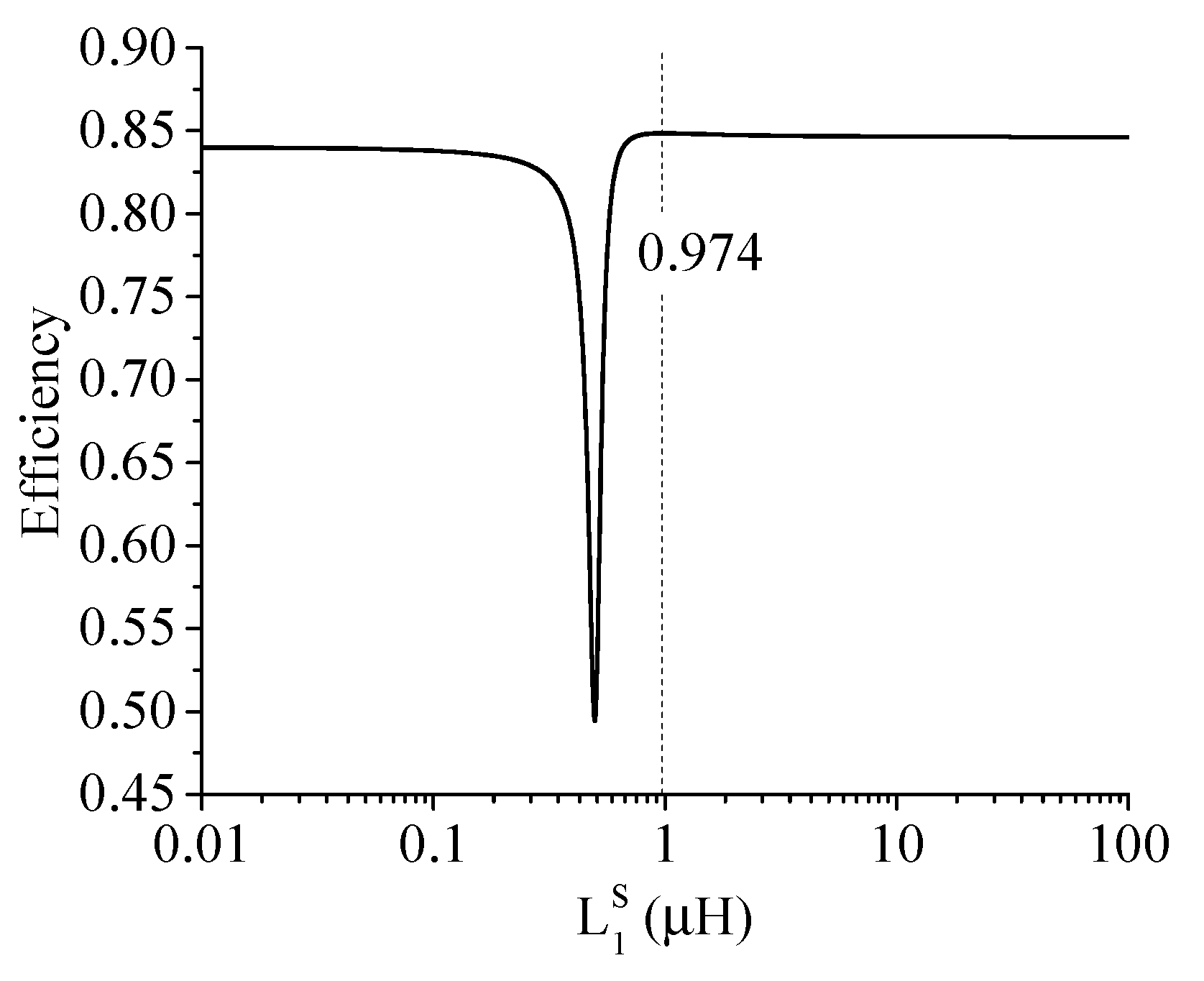
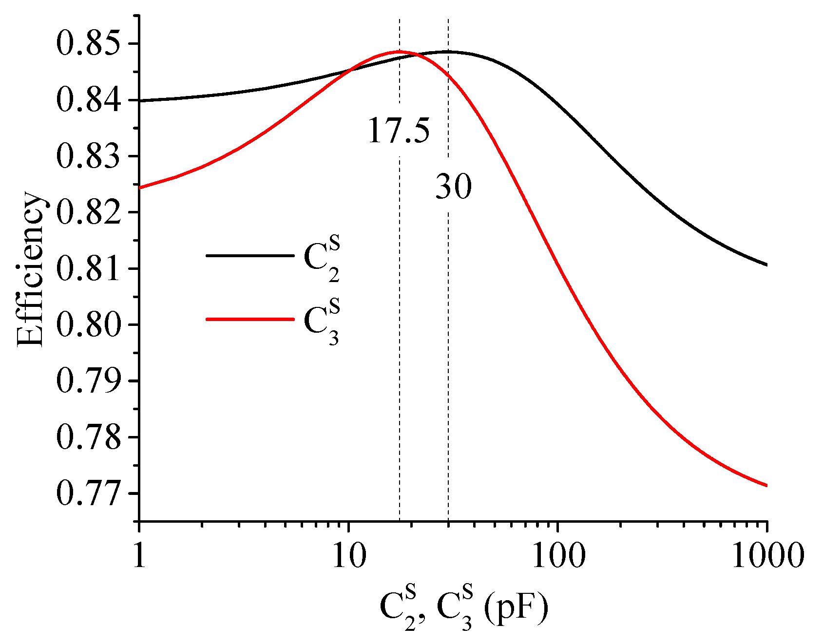
Regarding effect on the efficiency of the compensating shunt susceptances L 1 S , C 2 S , and C 3 S , this is investigated in Figure 6 and Figure 7. The simulated efficiency confirms that maximum efficiency is obtained by using the compensating shunt susceptances calculated by using the theoretical formulas.
Additionally, the simulation confirms that the shunt susceptances at the input ports eliminate the cross-coupling. For the circuit without the compensating shunt susceptances and no cross-coupling, the same maximum efficiency of 84.9% is reached.
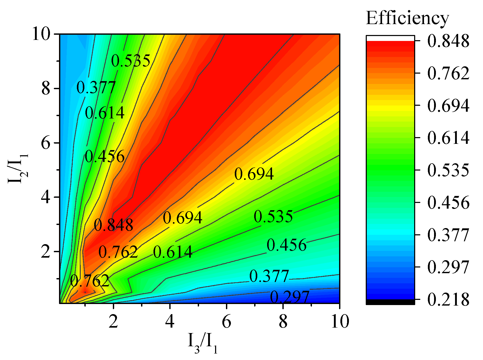
Finally, the effect of the amplitude of the input currents has been analyzed. The achieved results are summarized in Figure 8. It is observed that the efficiency is always lower than the optimal current distribution from Table 4 (i.e., I 2 / I 1 = 3 and I 3 / I 1 = 2 ). For example, if all input current sources are equal to 100 mA, an efficiency of 76.2% is attained.
The case of voltage sources has been also analyzed; in this case, by using Equation (57) and the values of Equation (59), the optimal voltage ratios can be determined, e.g.,
V 2 V 1 = b 02 g 22 b 01 g 11 = 2 .
Analogously, the optimal ration V 3 / V 1 = 4 is found. This is confirmed by circuital simulation results summarized in Figure 9.
In conclusion, circuital simulations confirm the data provided by the theory for the analyzed example: a maximum power-transfer efficiency is achieved for the optimal values of Table 4, calculated according to analytical derivation.

7. Conclusions

A general CPT system with any number of transmitters and a single receiver was optimized towards power-transfer efficiency. It was shown that in order to maximize the efficiency of a system with given wireless links and couplings, three conditions must be fulfilled simultaneously. First, the ratio of the input current sources is dependent on the coupling between each transmitter and the receiver, given by Equation (47). Secondly, the undesired cross-coupling between the transmitters themselves can be eliminated by adding appropriate shunt susceptances, given by Equation (41), at the input terminals. Finally, the optimal load is purely resistive, equal to Equation (55), if the receiver has no self-susceptance. If a self-susceptance is present at the receiver’s side, a compensating load susceptance is required.
Additionally, by conjugate-matching the internal shunt admittance of the generators, the maximum-efficiency solution coincides with the configuration that maximizes the output power.
It was shown that the maximum achievable efficiency η m a x , the optimal loads, and the optimal input currents are independent on the cross-coupling between the transmitters, since this unwanted cross-coupling can be entirely annihilated with the transmitter shunt susceptances B n S . As a result, it is possible to increase the system efficiency by adding more transmitters, and compensating every time for transmitter cross-coupling.
The expression for the extended kQ-factor for each transmitter–receiver link was determined, allowing an estimate of the maximum efficiency of the CPT system via the system kQ-product.
Finally, the analytical derivation was verified by simulation of an example CPT system with three transmitters and a single receiver. Measurements on a CPT setup with multiple transmitters are required to confirm the accuracy of the analytical results and are part of future research.

Author Contributions

Conceptualization, methodology, B.M., M.M.; validation, B.M., G.M., M.M.; writing–original draft preparation, B.M.; writing–review and editing, A.C., G.M., M.M. All authors have read and agreed to the published version of the manuscript.

Funding

This research received no external funding.

Acknowledgments

The authors would like to remember the colleague Franco Mastri who suddenly passed away on April 3rd, 2020. He was a great colleague and a profound scientist. Fundamental discussions and studies on the theoretical modelling of near-field WPT systems were of great inspiration also for the results presented in this work.

Conflicts of Interest

The authors declare no conflict of interest.

References

  1. Zhu, Q.; Zang, S.; Zou, L.J.; Zhang, G.; Su, M.; Hu, A.P. Study of coupling configurations of capacitive power transfer system with four metal plates. Wirel. Power Transf. 2019, 6, 97–112. [Google Scholar] [CrossRef]
  2. Wang, K.; Sanders, S. Contactless USB—A capacitive power and bidirectional data transfer system. In Proceedings of the IEEE Applied Power Electronics Conference and Exposition-APEC, Fort Worth, TX, USA, 16–20 March 2014; pp. 1342–1347. [Google Scholar]
  3. Hu, A.P.; Liu, C.; Li, H.L. A novel contactless battery charging system for soccer playing robot. In Proceedings of the IEEE 15th International Conference on Mechatronics and Machine Vision in Practice, Auckland, New Zealand, 2–4 December 2008; pp. 646–650. [Google Scholar]
  4. Culurciello, E.; Andreou, A.G. Capacitive inter-chip data and power transfer for 3-D VLSI. IEEE Trans. Circ. Syst. II Express Briefs 2006, 53, 1348–1352. [Google Scholar] [CrossRef]
  5. Mostafa, T.M.; Muharam, A.; Hattori, R. Wireless battery charging system for drones via capacitive power transfer. In Proceedings of the IEEE PELS Workshop on Emerging Technologies: Wireless Power Transfer (WoW), Chongqing, China, 20–22 May 2017; pp. 1–6. [Google Scholar]
  6. Sodagar, A.M.; Amiri, P. Capacitive coupling for power and data telemetry to implantable biomedical microsystems. In Proceedings of the IEEE 4th International IEEE/EMBS Conference on Neural Engineering, Antalya, Turkey, 29 April–2 May 2009; pp. 411–414. [Google Scholar]
  7. Jegadeesan, R.; Agarwal, K.; Guo, Y.X.; Yen, S.C.; Thakor, N.V. Wireless power delivery to flexible subcutaneous implants using capacitive coupling. IEEE Trans. Microw. Theory Tech. 2016, 65, 280–292. [Google Scholar] [CrossRef]
  8. Ramos, I.; Afridi, K.; Estrada, J.A.; Popović, Z. Near-field capacitive wireless power transfer array with external field cancellation. In Proceedings of the IEEE Wireless Power Transfer Conference (WPTC), Aveiro, Portugal, 5–6 May 2016; pp. 1–4. [Google Scholar]
  9. Miyazaki, M.; Abe, S.; Suzuki, Y.; Sakai, N.; Ohira, T.; Sugino, M. Sandwiched parallel plate capacitive coupler for wireless power transfer tolerant of electrode displacement. In Proceedings of the IEEE MTT-S International Conference on Microwaves for Intelligent Mobility (ICMIM), Nagoya, Japan, 19–21 March 2017; pp. 29–32. [Google Scholar]
  10. Dai, J.; Ludois, D.C. Wireless electric vehicle charging via capacitive power transfer through a conformal bumper. In Proceedings of the IEEE Applied Power Electronics Conference and Exposition (APEC), Charlotte, NC, USA, 15 March 2015; pp. 3307–3313. [Google Scholar]
  11. Sakai, N.; Itokazu, D.; Suzuki, Y.; Sakihara, S.; Ohira, T. One-kilowatt capacitive Power Transfer via wheels of a compact Electric Vehicle. In Proceedings of the IEEE Wireless Power Transfer Conference (WPTC), Aveiro, Portugal, 5–6 May 2016; pp. 1–3. [Google Scholar]
  12. Sinha, S.; Kumar, A.; Regensburger, B.; Afridi, K.K. A new design approach to mitigating the effect of parasitics in capacitive wireless power transfer systems for electric vehicle charging. IEEE Trans. Transp. Electr. 2019, 1040–1059. [Google Scholar] [CrossRef]
  13. Monti, G.; Che, W.; Wang, Q.; Costanzo, A.; Dionigi, M.; Mastri, F.; Mongiardo, M.; Perfetti, R.; Tarricone, L.; Chang, Y. Wireless power transfer with three-ports networks: Optimal analytical solutions. IEEE Trans. Circ. Syst. I Regul. Pap. 2016, 64, 494–503. [Google Scholar] [CrossRef]
  14. Ujihara, T.; Duong, Q.T.; Okada, M. kQ-product analysis of inductive power transfer system with two transmitters and two receivers. In Proceedings of the IEEE Wireless Power Transfer Conference, Taipei, Taiwan, 10–12 May 2017. [Google Scholar]
  15. Duong, Q.T.; Okada, M. kQ-product formula for multiple-transmitter inductive power transfer system. IEICE Electron. Express 2017, 14, 20161167. [Google Scholar] [CrossRef] [Green Version]
  16. Arakawa, T.; Goguri, S.; Krogmeier, J.V.; Kruger, A.; Love, D.J.; Mudumbai, R.; Swabey, M.A. Optimizing wireless power transfer from multiple transmit coils. IEEE Access. 2018, 6, 23828–23838. [Google Scholar] [CrossRef]
  17. Lang, H.D.; Sarris, C.D. Semidefinite relaxation-based optimization of multiple-input wireless power transfer systems. IEEE Trans. Microw. Theory Tech. 2017, 65, 4294–4306. [Google Scholar] [CrossRef]
  18. Lang, H.D.; Ludwig, A.; Sarris, C.D. Convex optimization of wireless power transfer systems with multiple transmitters. IEEE Trans. Antennas Propagat. 2014, 62, 4623–4636. [Google Scholar] [CrossRef]
  19. Monti, G.; Wang, Q.; Che, W.; Costanzo, A.; Mastri, F.; Mongiardo, M. Maximum wireless power transfer for multiple transmitters and receivers. In Proceedings of the IEEE MTT-S International Conference on Numerical Electromagnetic and Multiphysics Modeling and Optimization (NEMO), Beijing, China, 27–29 July 2016; pp. 1–3. [Google Scholar]
  20. Duong, Q.T.; Okada, M. Maximum efficiency formulation for inductive power transfer with multiple receivers. IEICE Electron. Express 2016, 13, 20160915. [Google Scholar] [CrossRef] [Green Version]
  21. Yoon, I.J.; Ling, H. Investigation of near-field wireless power transfer under multiple transmitters. IEEE Antennas Wirel. Propag. Lett. 2011, 10, 662–665. [Google Scholar] [CrossRef]
  22. Minnaert, B.; Stevens, N. Optimal analytical solution for a capacitive wireless power transfer system with one transmitter and two receivers. Energies 2017, 10, 1444. [Google Scholar] [CrossRef] [Green Version]
  23. Minnaert, B.; Mongiardo, M.; Costanzo, A.; Mastri, F. Maximum Efficiency Solution for Capacitive Wireless Power Transfer with N Receivers. Wirel. Power Transf. 2020, 1–11. [Google Scholar] [CrossRef]
  24. Huang, L.; Hu, A.P. Defining the mutual coupling of capacitive power transfer for wireless power transfer. Electron. Lett. 2015, 51, 1806–1807. [Google Scholar] [CrossRef]
  25. Hong, J.S.G.; Lancaster, M.J. Microstrip Filters for RF/Microwave Applications, 1st ed.; John Wiley & Sons: New York, NY, USA, 2001; pp. 235–253. [Google Scholar]
  26. Boyd, S.; Vandenberghe, L. Convex Optimization, 2nd ed.; Cambridge University Press: Cambridge, UK, 2004; p. 140. [Google Scholar]
  27. Ohira, T. Extended k-Q product formulas for capacitive-and inductive-coupling wireless power transfer schemes. IEICE Electron. Express 2014, 11, 20140147. [Google Scholar] [CrossRef] [Green Version]
  28. Minnaert, B.; Stevens, N. Single variable expressions for the efficiency of a reciprocal power transfer system. Int. J. Circ. Theory Appl. 2017, 10, 1418–1430. [Google Scholar] [CrossRef]
  29. Sugiyama, R.; Duong, Q.T.; Okada, M. kQ-product analysis of multiple-receiver inductive power transfer with cross-coupling. In Proceedings of the International Workshop on Antenna Technology: Small Antennas, Innovative Structures, and Applications (iWAT), Athens, Greece, 1–3 March 2017. [Google Scholar]
  30. Dionigi, M.; Mongiardo, M.; Monti, G.; Perfetti, R. Modelling of wireless power transfer links based on capacitive coupling. Int. J. Numer. Model. Electron. Netw. Dev. Fields 2017, 30, e2187. [Google Scholar] [CrossRef]
  31. Kracek, J.; Svanda, M. Analysis of Capacitive Wireless Power Transfer. IEEE Access. 2018, 7, 26678–26683. [Google Scholar] [CrossRef]
  32. Kim, D.H.; Ahn, D. Optimization of Capacitive Wireless Power Transfer System for Maximum Efficiency. J. Electr. Eng. Technol. 2020, 15, 343–352. [Google Scholar] [CrossRef]
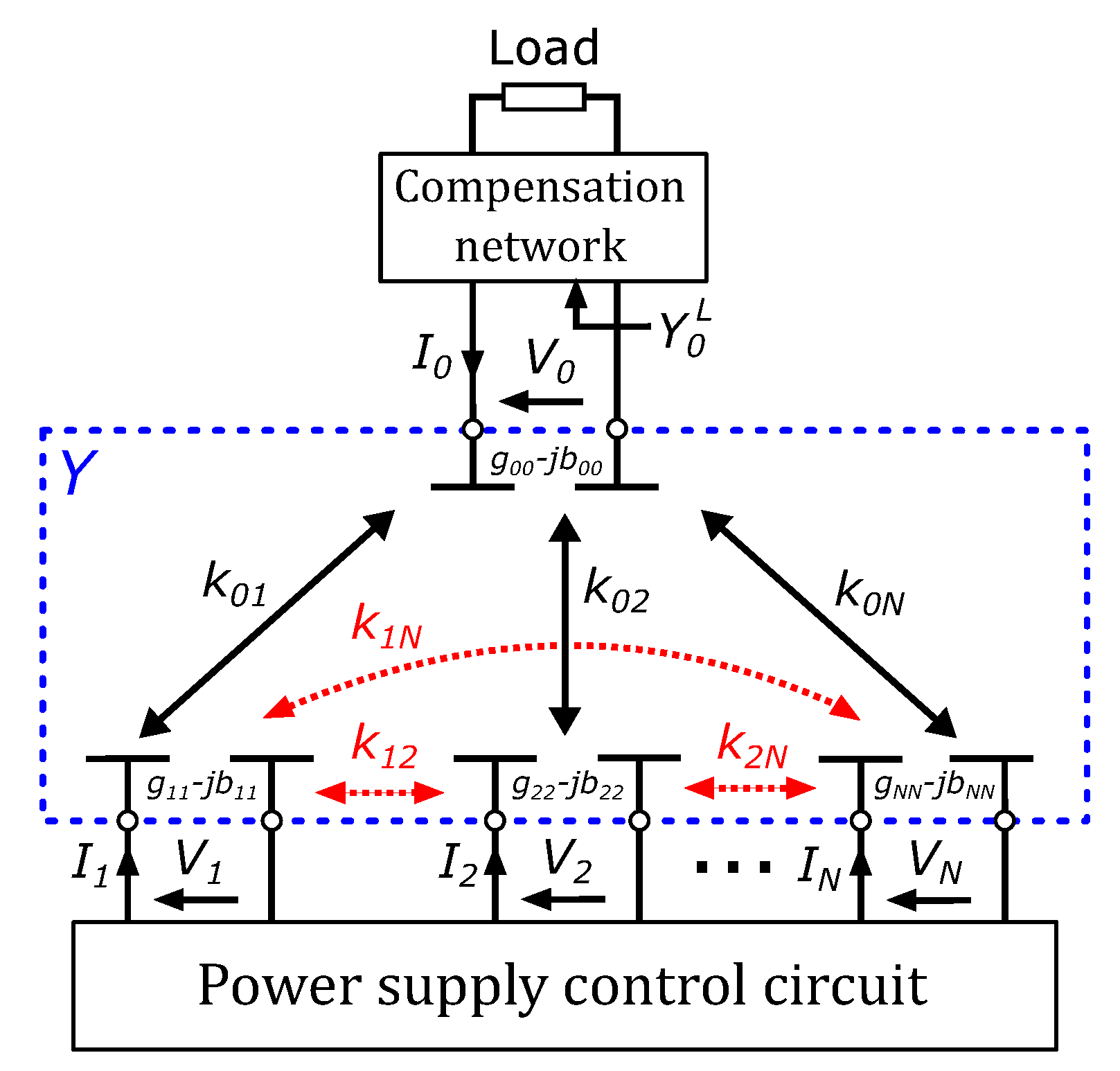
Figure 1. A general capacitive wireless power transfer system with N transmitters (bottom) and a single receiver (top). The (desired) electric couplings between transmitters and receiver are depicted by the full arrows. The undesired cross-couplings between the transmitters themselves are indicated by the dashed arrows.
Energies 13 03482 g001
Figure 2. Maximum-efficiency solution for (a) the transmitter ports with generator I n S and internal shunt admittance Y n S , and (b) the receiver port with the optimal load susceptance and load conductance.
Energies 13 03482 g002
Figure 3. (a) Equivalent circuit of a capacitive wireless power transfer system with 3 transmitters (left) and a single receiver (right). The (desired) electric couplings between transmitters and receiver are depicted by the full arrows. The (undesired) cross-couplings between transmitters themselves are indicated by the dashed arrows. (b) Applied equivalent circuit for the simulation of the capacitive coupling.
Energies 13 03482 g003
Figure 4. The simulated efficiency η as a function of varying load conductance for the given system of three transmitters and a single receiver. The load conductance is varied, while keeping the other system parameters at their optimal value.
Energies 13 03482 g004
Figure 5. The simulated efficiency η as a function of varying shunt load inductance for the given system of three transmitters and a single receiver. The load inductance is varied, while keeping the other system parameters at their optimal value.
Energies 13 03482 g005
Figure 6. The simulated efficiency η as a function of the compensating susceptance L 1 S . L 1 S is varied, while keeping the other system parameters at their optimal value.
Energies 13 03482 g006
Figure 7. The simulated efficiency η as a function of the compensating susceptance C 2 S and C 3 S . C 2 S (black curve) or C 3 S (red curve) is varied, while keeping the other system parameters at their optimal value.
Energies 13 03482 g007
Figure 8. The simulated efficiency η as a function of the ratio of the input currents. The efficiency is always lower than the optimal current distribution I 2 / I 1 = 3 and I 3 / I 1 = 2 . For example, if all input current sources are equal (i.e., I 2 / I 1 = 1 and I 3 / I 1 = 1 ), an efficiency of 76.2% is attained.
Energies 13 03482 g008
Figure 9. The simulated efficiency η as a function of the ratio of the input voltages.
Energies 13 03482 g009
Table 1. Given network simulation parameters for the analyzed numerical example.
QuantityValueQuantityValue
f 0 10.0 MHz I 1 S 100 mA
g 00 1.00 mS C 0 350 pF
g 11 1.00 mS C 1 350 pF
g 22 1.50 mS C 2 300 pF
g 33 0.50 mS C 3 275 pF
C 00 500 pF C 11 500 pF
Table 2. Coupling factors of the analyzed example.
Desired CouplingsValueUndesired CouplingsValue
k 01 14.3% k 12 6.2%
k 02 46.3% k 13 16.1%
k 03 32.2% k 23 3.5%
Table 3. Calculated network simulation parameters for the example capacitive power transfer (CPT) system.
QuantityValueQuantityValue
L 0 724 nH α 1 3.1
L 1 724 nH α 2 7.7
L 2 844 nH α 3 8.9
L 3 921 nH α N 12.2
Table 4. Calculated values for the maximum efficiency solution.
QuantityValueQuantityValue
I 2 S 300 mA I 3 S 200 mA
G 0 L , o p t ( R 0 L , o p t )12.2 mS (81.9  Ω ) L 1 S 974 nH
L 0 L , o p t 506 nH C 2 S 30.0 pF
η m a x 84.9% C 3 S 17.5 pF