Modeling of Selected Lighting Parameters of LED Panel


Abstract
1. Introduction
2. Results of Studies
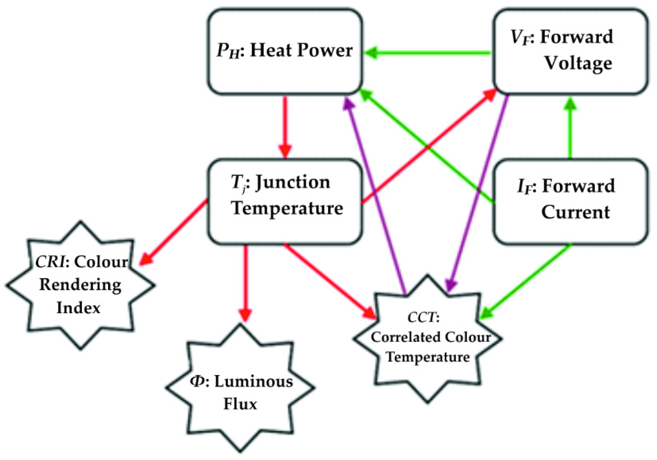
2.1. The Effect of Junction Temperature on the Lighting Parameters of a Single LED Source
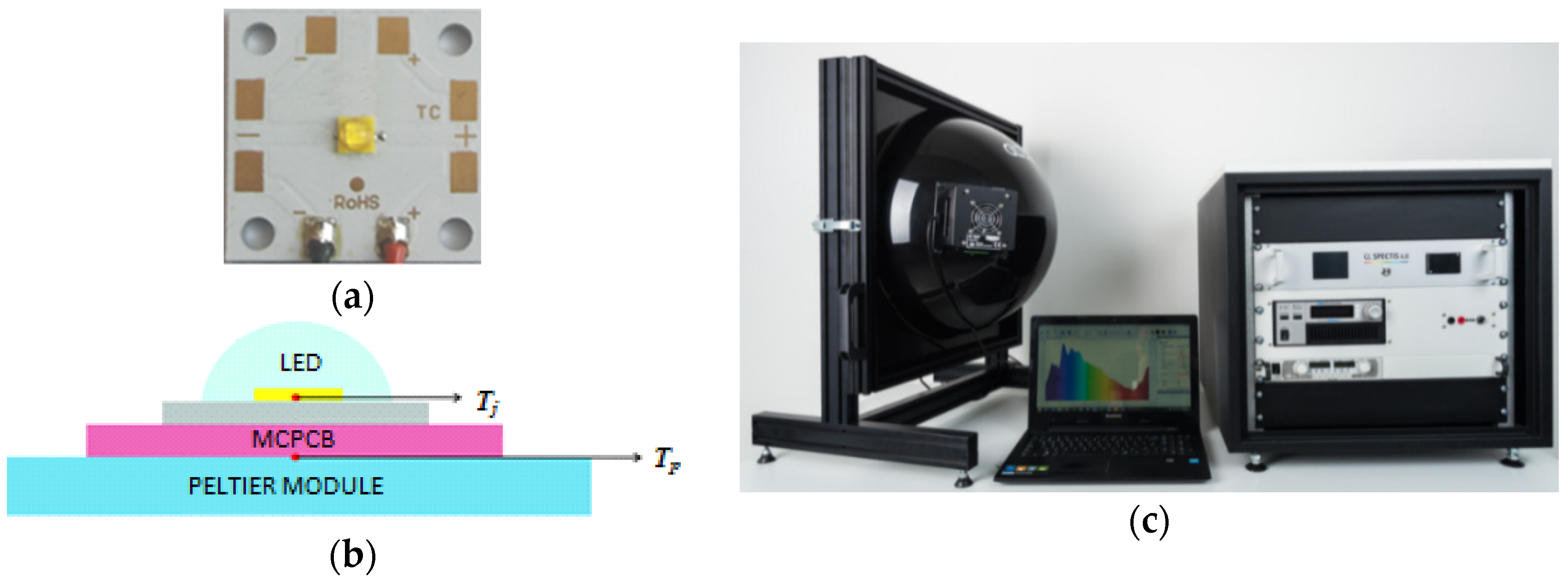
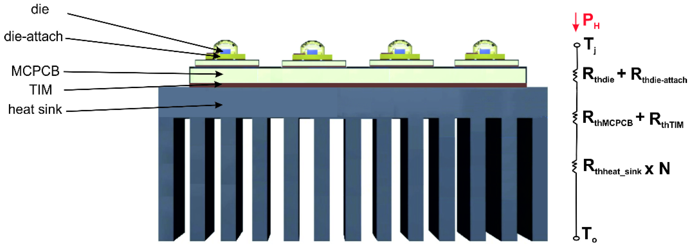
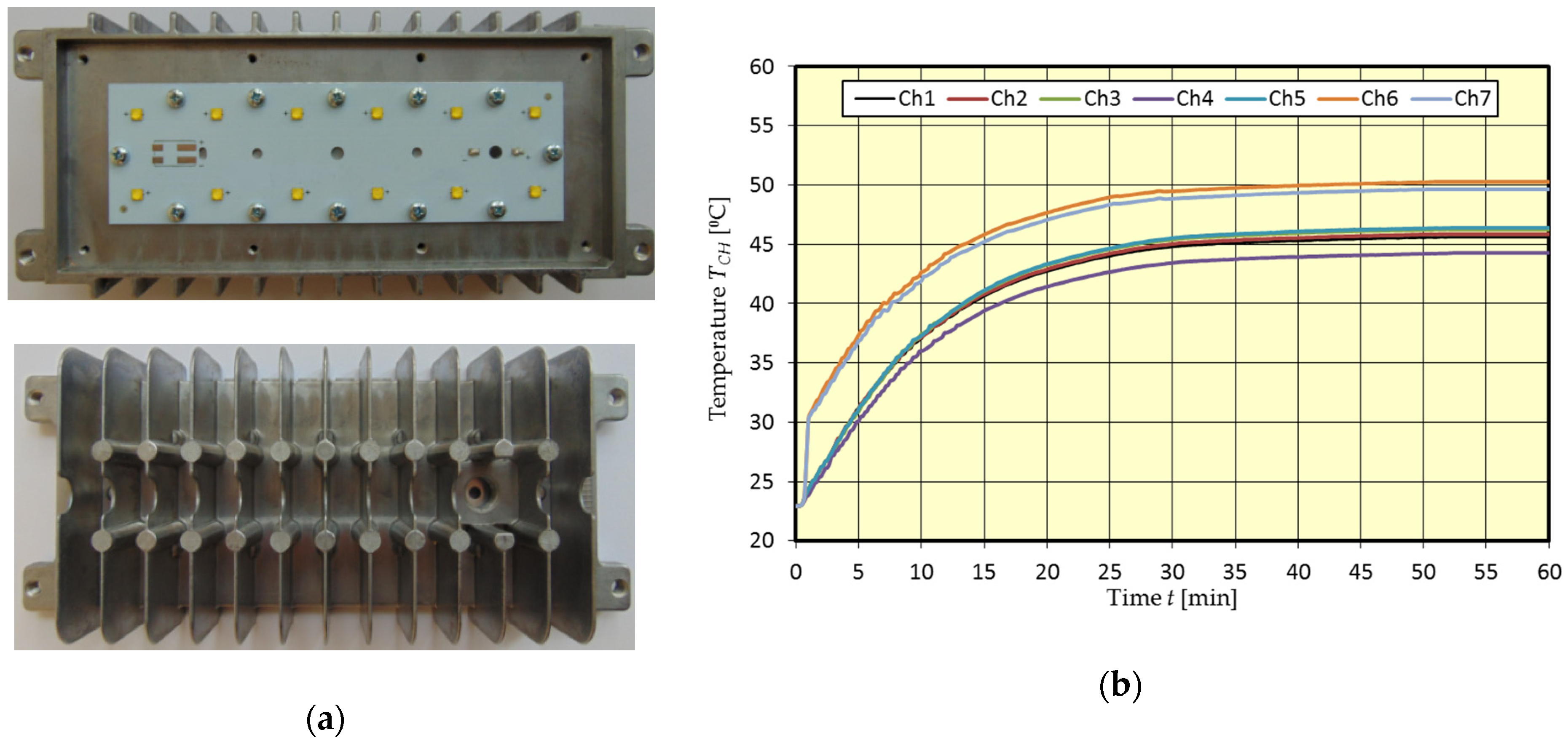
2.2. Thermal Modeling of the LED Panel
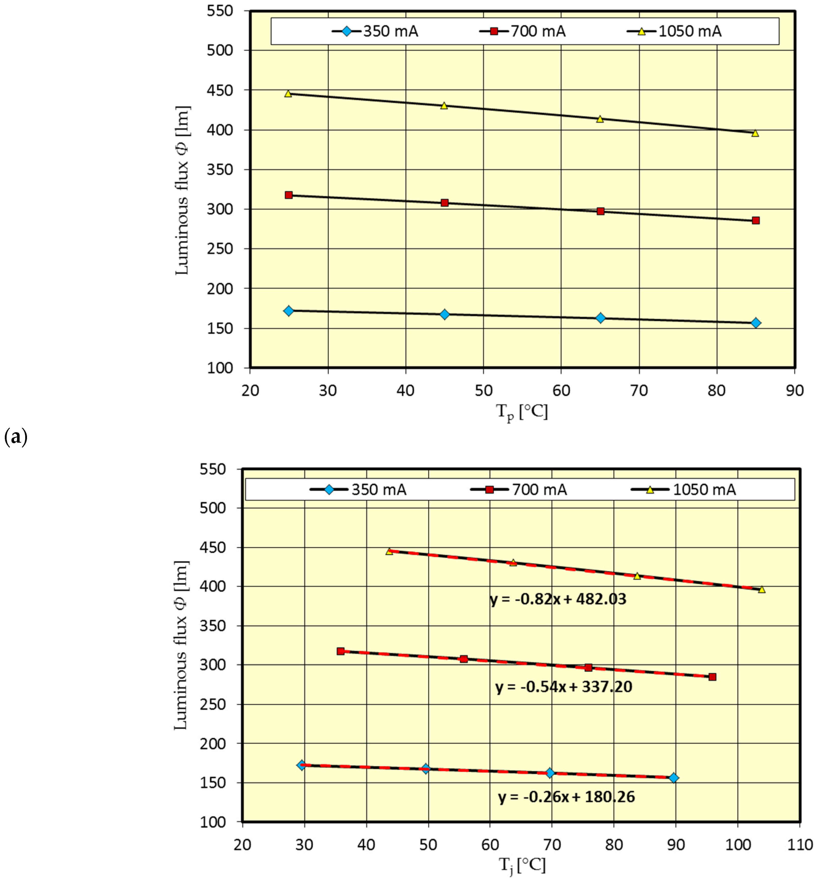
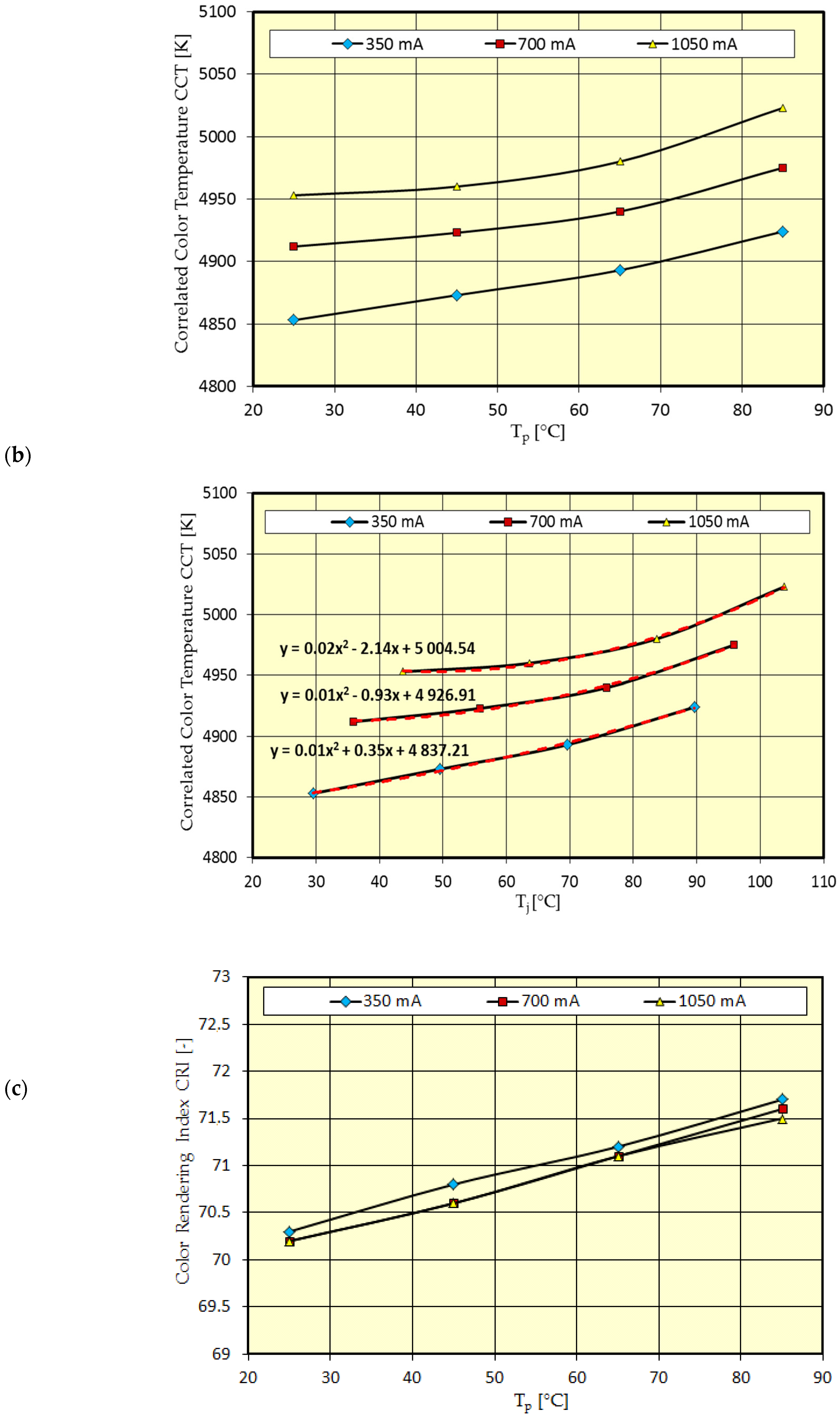
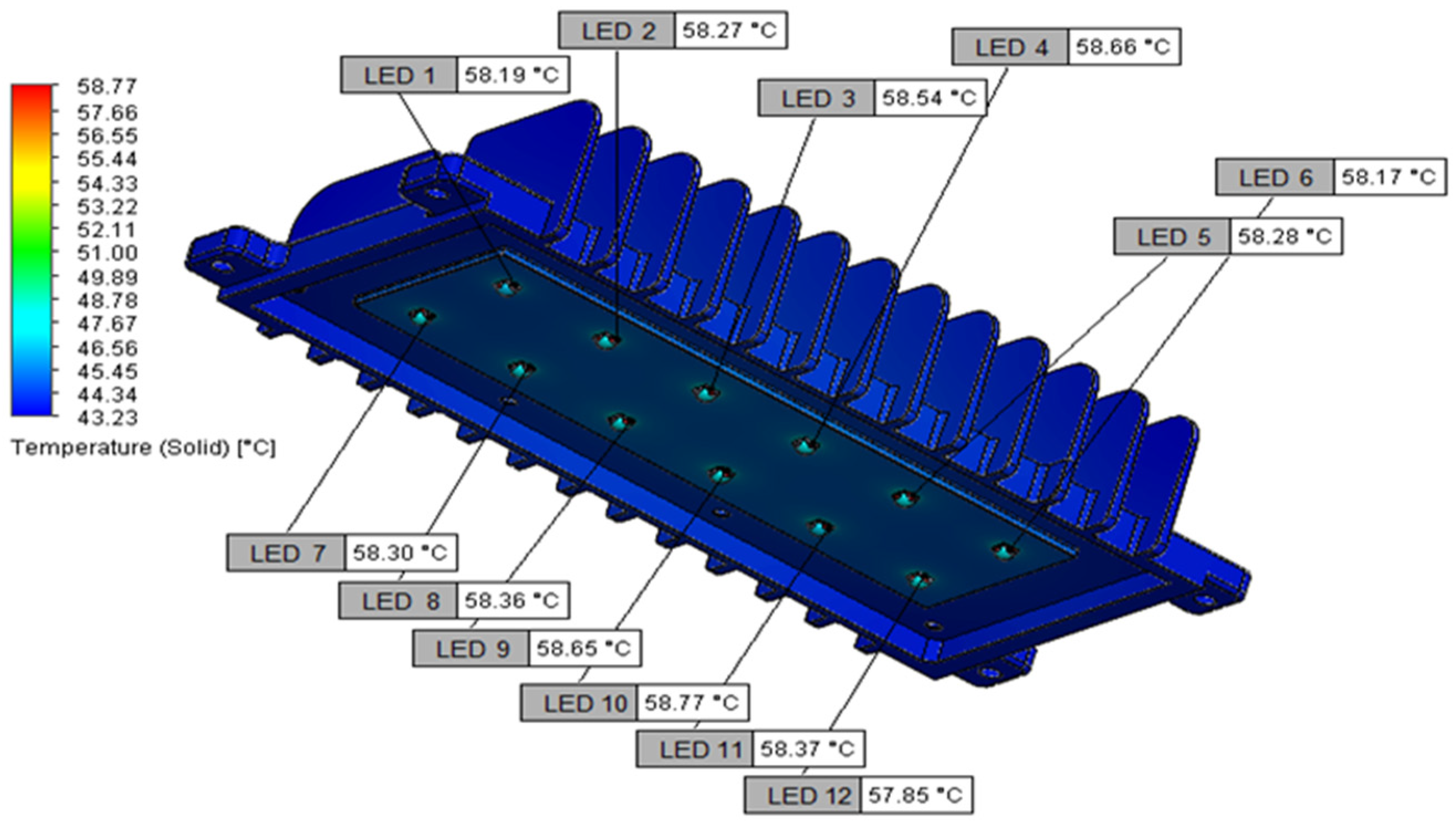
2.3. Modeling of LED Panel Luminous Parameters
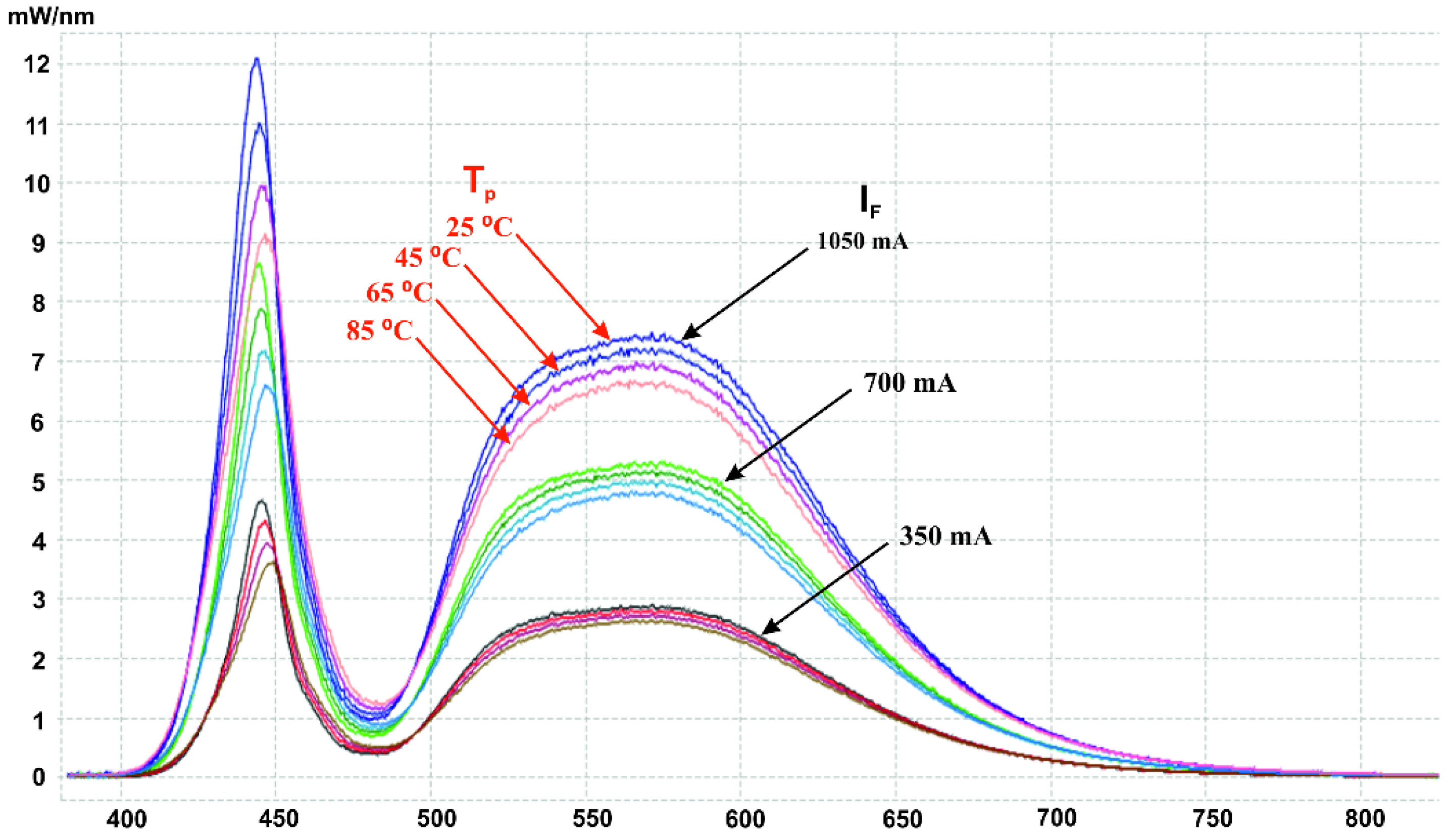
- luminous flux Φ
- correlated colour temperature CCT
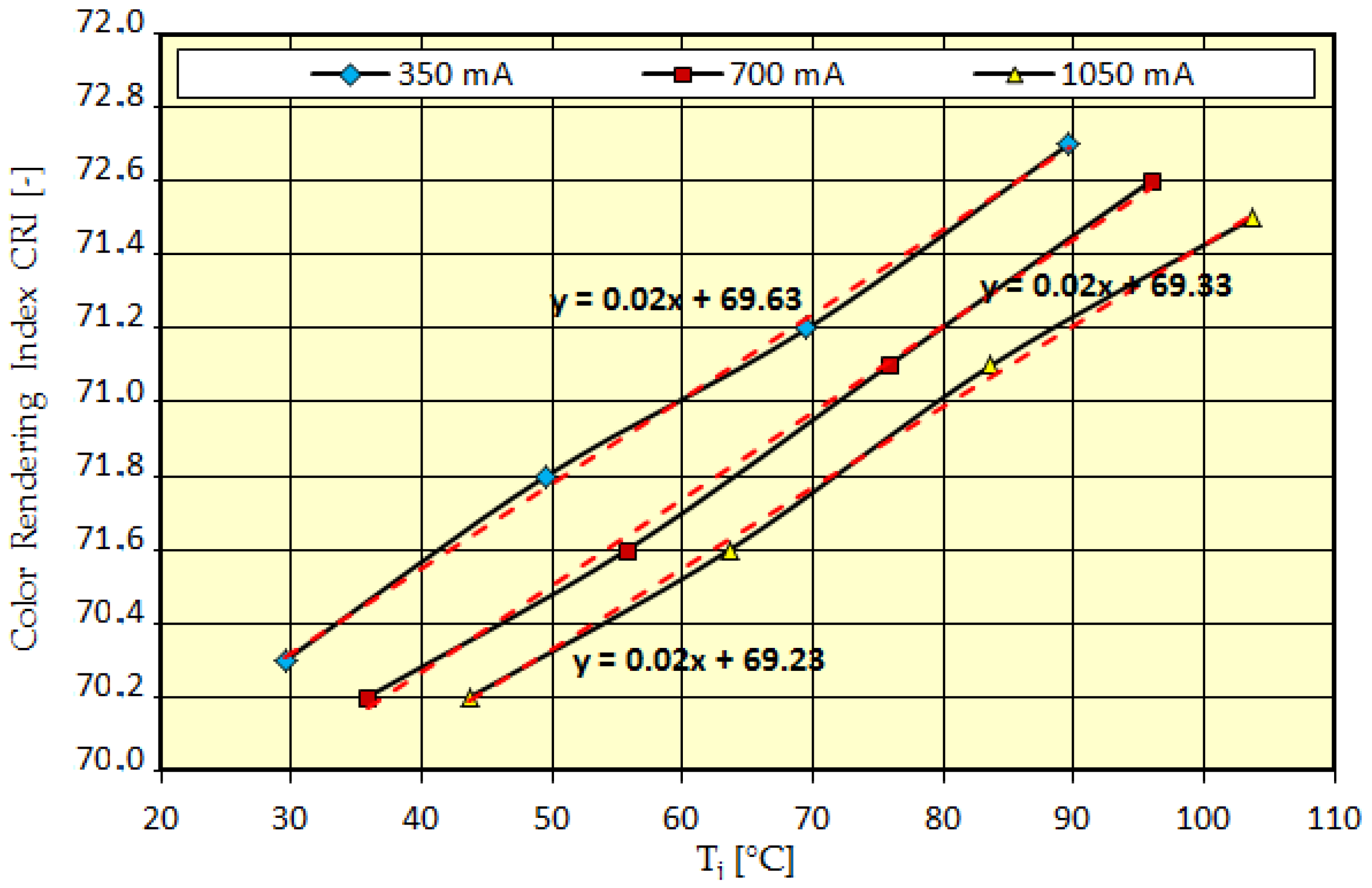
- colour rendering index CRI
3. Conclusions
Author Contributions
Funding
Conflicts of Interest
Nomenclature
| ε | emissivity factor |
| ηo | optical efficiency |
| Φ | luminous flux |
| CCT | correlated color temperature |
| CRI | color rendering index |
| HBH | heatsink base height |
| Hf | heat sink fin height |
| Hp | LED panel height |
| IF | forward current |
| k | thermal conductivity |
| Lp | LED panel length |
| Pe | electrical power |
| PH | heat power |
| Po | optical power |
| Rthj-c | LED thermal resistance junction to case |
| Ta | ambient temperature |
| Tj | junction temperature |
| Tp | peltier module temperature |
| VF | forward voltage |
| Wp | LED panel width |
References
- Chen, H.; Tan, S.; Hui, S. Analysis and modeling of high-power phosphor-coated white light-emitting diodes with a large surface area. IEEE Trans. Power Electron. 2015, 30, 3334–3344. [Google Scholar] [CrossRef]
- Acuna, P.C.; Leyre, J.; Audenaert, J.; Meuret, Y.; Deconinck, G.; Hanselaer, P. Impact of geometrical and optical parameters on the performance of a cylindrical remote phosphor LED. IEEE Photonics J. 2015, 7. [Google Scholar] [CrossRef]
- Jagerbrand, A. LED (Light-Emitting Diode) road lighting in practice: An evaluation of compliance with regulations and improvements for further energy savings. Energies 2016, 9, 357. [Google Scholar] [CrossRef]
- Raychiy, J.; Ming-Shiou, T.; Ching-Cherng, S. Novel optical lens design with a light scattering freeform inner surface for LED down light illumination. Opt. Express 2015, 23, 16715–16722. [Google Scholar]
- Różowicz, A.; Leśko, M.; Wachta, H. The Technical Possibilities of Losses Reduction in the LED Optical Systems. In Proceedings of the 2016 IEEE Lighting Conference of the Visegrad Countries (LUMEN V4), Karpacz, Poland, 13–16 September 2016. Art. no. 978-1-5090-3305-8/16. [Google Scholar]
- Zissis, G. Energy Consumption and Environmental and Economic Impact of Lighting: The Current Situation. In Handbook of Advanced Lighting Technology; Springer: Cham, Switzerland, 2016; pp. 1–13. [Google Scholar]
- Leśko, M.; Różowicz, A.; Wachta, H.; Różowicz, S. Adaptive luminaire with variable luminous intensity distribution. Energies 2020, 13, 721. [Google Scholar] [CrossRef]
- Czyżewski, D. Comparison of luminance distribution on the lighting surface of power LEDs. Photonics Lett. Pol. 2019, 11, 118–120. [Google Scholar] [CrossRef]
- Liu, L.; Keoleian, G.; Saitou, K. Replacement policy of residential lighting optimized for cost, energy, and greenhouse gas emissions. Environ. Res. Lett. 2017, 12, 114034. [Google Scholar] [CrossRef]
- Barroso, A.; Dupuis, P.; Alonso, C.; Jammes, B.; Seguier, L.; Zissis, G. A Characterization Framework to Optimize LED Luminaire’s Luminous Efficacy. In Proceedings of the 2015 IEEE Industry Applications Society Annual Meeting, Dallas, TX, USA, 18–22 October 2015; pp. 905–913. [Google Scholar]
- Juntunen, E.; Tetri, E.; Tapaninen, O.; Yrjänä, S.; Kondratyev, V.; Sitomaniemi, A.; Siirtola, H.; Sarjanoja, E.; Aikio, J.; Heikkinen, V. A smart LED luminaire for energy savings in pedestrian road lighting. Lighting Res. Technol. 2015, 47, 103–115. [Google Scholar] [CrossRef]
- Czyżewski, D. Research on Luminance Distributions of Chip-On-Board Light-Emitting Diodes. Crystals 2019, 9, 645. [Google Scholar] [CrossRef]
- Różowicz, A.; Baran, K.; Wachta, H. Radiation studies of the illumination lighting luminaires with LED technology. In Proceedings of the 6th IEEE Lighting Conference of the Visegrad Group Countries, Karpacz, Poland, 13–16 September 2016; pp. 1–4. [Google Scholar]
- Lasance, C.; Poppe, A. Thermal Management for LED Applications; Springer Science, Business Media: New York, NY, USA, 2014. [Google Scholar]
- Yang, K.; Chung, C.; Tu, C.; Wong, C.; Yang, T.; Lee, M. Thermal spreading resistance characteristics of a high power light emitting diode module. Appl. Ther. Eng. 2014, 70, 361–368. [Google Scholar] [CrossRef]
- Hui, S.; Li, S.; Tao, X.; Chen, W.; Ng, W. A novel passive offline LED driver with long lifetime. IEEE Trans. Power Electron. 2010, 25, 2665–2672. [Google Scholar] [CrossRef]
- Hsu, H.-C.; Huang, Y.-C. Numerical simulation and experimental validation for the thermal analysis of a compact led recessed downlight with heat sink design. Appl. Sci. 2017, 7, 4. [Google Scholar] [CrossRef]
- Ye, H.; Koh, S.W.; van Zeijl, H.W.; Gielen, S.; Zhang, G. A review of passive thermal management of LED module. J. Semicond. 2011, 32. [Google Scholar] [CrossRef]
- Guo, Y.; Pan, K.; Ren, G.; Yuan, F. Research on LED Temperature Characteristic and Thermal Analysis at Low Temperatures. In Proceedings of the International Conference on Electronic Packaging Technology & High Density Packaging, Guilin, China, 13–16 August 2012; pp. 1411–1415. [Google Scholar]
- Scheepers, G.; Visser, J. Detailed Thermal Modeling of High Powered LEDs. In Proceedings of the 25th Annual IEEE Semiconductor Thermal Measurement and Management Symposium, San Jose, CA, USA, 15–19 March 2009; pp. 87–91. [Google Scholar]
- Pounds, D.; Bonner, R. High heat flux heat pipes embedded in metal core printed circuit boards for LED thermal management. In Proceedings of the 14th Intersociety Conference on Thermal and Thermomechanical Phenomena in Electronic Systems (ITherm), Orlando, FL, USA, 27–30 May 2014; pp. 267–271. [Google Scholar]
- Yurtseven, M.B.; Mete, S.; Onaygil, S. The effects of temperature and driving current on the key parameters of commercially available high-power white LEDs. Lighting Res. Technol. 2016, 48, 943–965. [Google Scholar] [CrossRef]
- Baran, K.; Różowicz, A.; Wachta, H.; Różowicz, S.; Mazur, D. Thermal analysis of the factors influencing junction temperature of LED panel sources. Energies 2019, 12, 3941. [Google Scholar] [CrossRef]
- Shen, Q.; Sun, D.; Xu, Y.; Jin, T.; Zhao, X. Orientation effects on natural convection heat dissipation of rectangular fin heat sinks mounted on LEDs. Int. J. Heat Mass Transf. 2014, 75, 462–469. [Google Scholar] [CrossRef]
- Tzeng, S.; Jeng, T.; Wang, Y. The cooling design of a high-speed rotating axis with ribbed turbulators. IJETI 2013, 3, 38–48. [Google Scholar]
- Costa, V.; Lopes, A. Improved radial heat sink for led lamp cooling. Appl. Ther. Eng. 2014, 70, 131–138. [Google Scholar] [CrossRef]
- Huang, Y.-S.; Luo, W.-C.; Wang, H.-C.; Feng, S.-W.; Kuo, C.-T.; Lu, C.-M. How smart LEDs lighting benefit color temperature and luminosity transformation. Energies 2017, 10, 518. [Google Scholar] [CrossRef]
- Ron, H. Photo-Electro-Thermal Theory for LED Systems. In Basic Theory and Application; Cambridge University Press: Cambridge, UK, 2017. [Google Scholar]
- Hyunjong, K.; Kyoung, J.; Yeonwon, L. Thermal Performance of Smart Heat Sinks for Cooling High Power LED Modules. In Proceedings of the 13th IEEE Intersociety Conference on Thermal and Thermomechanical Phenomena in Electronic Systems, San Diego, CA, USA, 30 May–1 June 2012. [Google Scholar]
- Gupta, D.; Venkataraman, V.; Nimje, R. CFD& Thermal Analysis of Heat Sink and its Application in CPU. Int. J. Emerg. Technol. Adv. Eng. 2014, 4, 198–202. [Google Scholar]
- Cao, J. Study on Three-imensional Numerical Simulation of the Influence of Fin Spacing on the Power of Heat Sink and Heat Dissipation. In Proceedings of the Asia-Pacific Power and Energy Engineering Conference, Wuhan, China, 25–28 March 2011. [Google Scholar]
- Yieang, H.; Shengnan, S.; Hui, L.; Yunjie, G. Improved Thermal Design of Fin Heat Sink for High-Power LED Lamp Cooling. In Proceedings of the 17th International Conference on Electronic Packaging Technology, Wuhan, China, 16–19 August 2016; pp. 1069–1074. [Google Scholar]
- Min, W.; Seung, W.; Yongchan, K. Optimal thermal design of a horizontal fin heat sink with a modified-opening model mounted on an LED module. Appl. Therm. Eng. 2015, 91, 105–115. [Google Scholar]
- Teeba, N.; Anithambigai, P.; Dinash, K.; Mutharasu, D. Influence of the Heat Sink Orientation and Fins Arrangement on the Thermal Behavior of High Power LED. In Proceedings of the The 3rd Asia Symposium on Quality Electronic Design, Kuala Lumpur, Malaysia, 19–20 July 2011; pp. 21–24. [Google Scholar]
- Rong, W.; Jung, W. Analyzing the structural designs and thermal performance of nonmetal lighting devices of LED bulbs. Int. J. Heat Mass Transf. 2016, 99, 750–761. [Google Scholar]
- Mawby, P.A.; Igic, P.M.; Towers, M.S. Physically based compact device models for circuit modelling applications. Microelectr. J. 2001, 32, 433–447. [Google Scholar] [CrossRef]
- Menozzi, R.; Cova, P.; Delmonte, N.; Giuliani, F.; Sozzi, G. Thermal and electrothermal modeling of components and systems: Review of the research at the University of Parma. Facta Univ. Ser. Electron. Energetics 2015, 28, 325–344. [Google Scholar] [CrossRef]
- Janicki, M.; Torzewicz, T.; Ptak, P.; Raszkowski, T.; Samson, A.; Górecki, K. Parametric compact thermal models of power LEDs. Energies 2019, 12, 1724. [Google Scholar] [CrossRef]
- Poppe, A. Simulation of LED based luminaires by using multi-domain compact models of LEDs and compact thermal models of their thermal environment. Microelectron. Reliab. 2017, 72, 65–74. [Google Scholar] [CrossRef]
- Chen, H.; Lin, S.; Xiong, C. Analysis and modeling of thermal effect and optical characteristic of LED systems with parallel plate-fin heatsink. IEEE Photonics J. 2017, 9. [Google Scholar] [CrossRef]
- Cuntala, J.; Kondelova, A.; Hock, O.; Pridala, M. Electro-Thermal Modeling of Power LED Using.COMSOL Environment. In Proceedings of the 11th International Conference ELEKTRO, Strbske Pleso, Slovakia, 16–18 May 2016; pp. 127–130. [Google Scholar]
- GL Opti Spheres. Available online: http://www.gloptic.com/wpcontent/uploads/2018/08/200931_Technical-Datasheet_SPHEREs.pdf (accessed on 3 January 2020).
- GL Spectis 6,0. Available online: http://www.gloptic.com/wp-content/uploads/2018/08/200930_Technical-Datasheet_SPECTIS-6-0.pdf (accessed on 3 January 2020).
- 5305 TECSource Arroy Instruments. Available online: http://www.arroyoinstruments.com/products/5305#tabs (accessed on 3 January 2020).
- Houser, K.; Mistrick, K.; Steffy, G.; Dlaura, D. The Lighting Handbook: Reference and Application, 10th ed.; Illuminating Engineering Society of North America (IES): New York, NY, USA, 2011. [Google Scholar]
- Liu, S.; Luo, X. LED Packaging for Lighting Applications: Design, Manufacturing and Testing; John Wiley & Sons Pte Ltd.: Singapore, 2011. [Google Scholar]
- Min, S. Thermal Analysis of High Power LED Arrays. Ph.D. Thesis, Georgia Institute of Technology, Atlanta, GA, USA, 2009. [Google Scholar]
- Palisoc, A.; Lee, C. Thermal-properties of the multilayer infinite-plate structure. J. Appl. Phys. 1988, 64, 410–415. [Google Scholar] [CrossRef]
- Masana, F. A new approach to the dynamic thermal modelling of semiconductor packages. Microelectron. Reliab. 2001, 41, 901–912. [Google Scholar] [CrossRef]
- Muzychka, Y.; Culham, R.; Yovanovich, M. Thermal spreading resistance of eccentric heat sources on rectangular flux channels. ASME J. Electron. Packag. 2003, 125, 178–185. [Google Scholar] [CrossRef]
- FloEFD. Technical Reference, Software Version 16, Mentor Graphics; Mentor Graphics Corporation: Wilsonville, OR, USA, 2016. [Google Scholar]
- Chein, R.; Chen, J. Numerical study of the inlet/outlet arrangement effect on microchannel heat sink performance. Int. J. Ther. Sci. 2009, 48, 1627–1638. [Google Scholar] [CrossRef]
- Della Torre, A.; Motenegro, G.; Onorati, A.; Khadilkar, S.; Icarelli, R. Multi-scale CFD modeling of plate heat exchangers including O set-strip fins and Dimple-Type Turbulators for automotive applications. Energies 2019, 12, 2965. [Google Scholar] [CrossRef]
- FloEFD Engineering Database. Available online: https://www.mentor.com/products/mechanical/floefd/ (accessed on 3 January 2020).
- Torzewicz, T.; Baran, K.; Raszkowski, T.; Samson, A.; Wachta, H.; Napieralski, A. Compact Thermal Modeling of Power LED Light Source. In Proceedings of the IEEE 30th International Conference on Microelectronics (MIEL), Nis, Serbia, 9–11 October 2017; pp. 157–160. [Google Scholar]
- JEDEC STANDARD. Transient Dual Interface Test Method for the Measurement of the Thermal Resistance Junction-to-Case of Semiconductor Devices with Heat Flow through a Single Path; JESD51-14; JEDEC Solid State Technology Association: Arlington, VA, USA, 2010. [Google Scholar]
- Baran, K.; Wachta, H.; Leśko, M.; Różowicz, A. Research on thermal resistance Rthj-c of high power semiconductor light sources. In Proceedings of the 15th Conference on Computational Technologies in Engineering, AIP Conference Proceedings 2078, Mikołajki, Poland, 16–19 October 2018; p. 020047. [Google Scholar]
- L200-TC Labfacility 8-Channel Laboratory Temperature Monitor. Available online: https://www.labfacility.com/media/productattach/d/a/datasheet_-_l200.pdf (accessed on 3 January 2020).
- Konica Minolta Spectroradiometer CS-2000. Available online: https://www.konicaminolta.com/instruments/download/instruction_manual/display/pdf/cs-2000-2002a_instruction_eng.pdf (accessed on 3 January 2020).


| Current IF (mA) | Temperature Tp (°C) | Electrical Power Pe (W) | Optical Power Po (W) | Heat Power PH (W) | Optical Efficiency ηo (%) |
|---|---|---|---|---|---|
| 350 | 25 | 1.01 | 0.50 | 0.51 | 49.83 |
| 45 | 0.99 | 0.49 | 0.50 | 49.39 | |
| 65 | 0.98 | 0.48 | 0.50 | 48.69 | |
| 85 | 0.97 | 0.46 | 0.51 | 47.70 | |
| 700 | 25 | 2.13 | 0.94 | 1.19 | 43.92 |
| 45 | 2.10 | 0.91 | 1.19 | 43.36 | |
| 65 | 2.08 | 0.88 | 1.20 | 42.54 | |
| 85 | 2.06 | 0.85 | 1.18 | 41.52 | |
| 1050 | 25 | 3.35 | 1.33 | 2.02 | 39.62 |
| 45 | 3.30 | 1.29 | 2.01 | 38.94 | |
| 65 | 3.26 | 1.24 | 2.02 | 38.09 | |
| 85 | 3.22 | 1.19 | 2.03 | 37.04 |
| Layer | Material | Thickness (mm) | Thermal Conductivity k (W/m∙K) | Thermal Resistance Rthj-c (°C/W) |
|---|---|---|---|---|
| Heat sink | Aluminum 5052 | 4 | 140 | - |
| TIM | Thermal paste | 0.1 | 3 | - |
| MCPCB | Aluminum 5052 | 1.5 | 140 | |
| Dielectric | 0.1 | 2 | - | |
| Copper | 0.035 | 400 | ||
| Soldering | 96.5Sn3.5Ag | 0.1 | 33 | |
| LED source | - | - | - | 8.6 IF = 350 mA |
| 8.6 IF = 700 mA | ||||
| 8.8 IF = 1050 mA | ||||
| Lens | Epoxy resin | - | 0.2 | - |
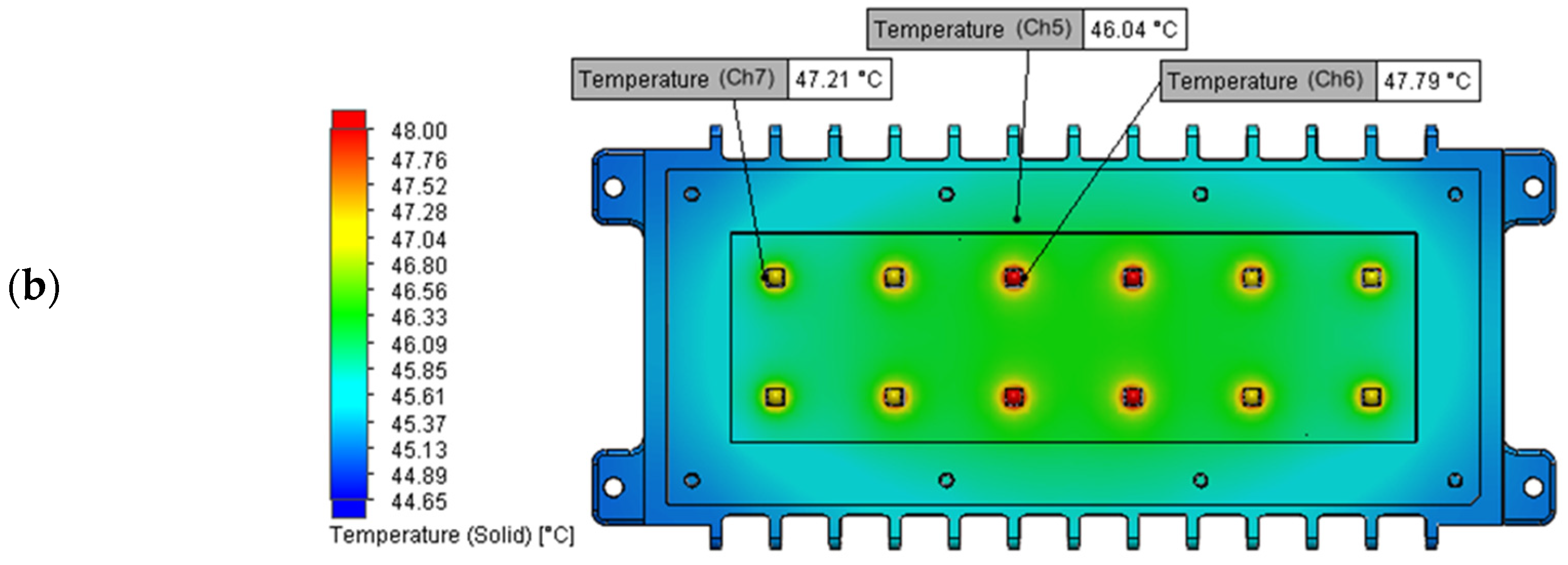
| IF [mA] | Ch1 | Ch2 | Ch3 | Ch4 | Ch5 | Ch6 | Ch7 | |
|---|---|---|---|---|---|---|---|---|
| 350 | Simulation result [°C] | 34.99 | 34.86 | 35.02 | 34.87 | 35.09 | 35.90 | 35.61 |
| Real measurement [°C] | 35.53 | 35.66 | 35.75 | 34.76 | 35.74 | 37.46 | 37.3 | |
| Error [%] | 1.52 | 2.25 | 2.05 | 0.32 | 1.82 | 4.17 | 4.54 | |
| 700 | Simulation result [°C] | 45.89 | 45.60 | 45.87 | 45.44 | 46.04 | 47.79 | 47.21 |
| Real measurement [°C] | 45.62 | 45.86 | 46.25 | 44.27 | 46.4 | 50.26 | 49.65 | |
| Error [%] | 0.60 | 0.57 | 0.83 | 2.65 | 0.78 | 4.92 | 4.92 | |
| 1050 | Simulation result [°C] | 55.98 | 55.49 | 56.14 | 55.40 | 56.45 | 60.2 | 59.1 |
| Real measurement [°C] | 55.31 | 56.04 | 56.43 | 53.46 | 57.02 | 63.14 | 62.2 | |
| Error [%] | 1.22 | 0.99 | 0.52 | 3.63 | 1.00 | 4.66 | 4.92 |
| IF = 350 mA | IF = 700 mA | |||||||
|---|---|---|---|---|---|---|---|---|
| Tj [°C] | Φ [lm] | CCT [K] | CRI [-] | Tj [°C] | Φ [lm] | CCT [K] | CRI [-] | |
| LED 1 | 40.66 | 169.69 | 4867.97 | 70.44 | 58.19 | 305.78 | 4906.65 | 70.49 |
| LED 2 | 40.73 | 169.67 | 4868.05 | 70.44 | 58.27 | 305.73 | 4906.67 | 70.50 |
| LED 3 | 40.84 | 169.64 | 4868.18 | 70.45 | 58.54 | 305.59 | 4906.74 | 70.50 |
| LED 4 | 40.89 | 169.63 | 4868.24 | 70.45 | 58.66 | 305.52 | 4906.77 | 70.50 |
| LED 5 | 40.73 | 169.67 | 4868.05 | 70.44 | 58.28 | 305.73 | 4906.68 | 70.50 |
| LED 6 | 40.65 | 169.69 | 4867.96 | 70.44 | 58.17 | 305.79 | 4906.65 | 70.49 |
| LED 7 | 40.71 | 169.68 | 4868.03 | 70.44 | 58.30 | 305.72 | 4906.68 | 70.50 |
| LED 8 | 40.77 | 169.66 | 4868.10 | 70.45 | 58.36 | 305.69 | 4906.69 | 70.50 |
| LED 9 | 40.89 | 169.63 | 4868.24 | 70.45 | 58.65 | 305.53 | 4906.76 | 70.50 |
| LED 10 | 40.94 | 169.62 | 4868.30 | 70.45 | 58.77 | 305.46 | 4906.79 | 70.51 |
| LED 11 | 40.77 | 169.66 | 4868.10 | 70.45 | 58.37 | 305.68 | 4906.70 | 70.50 |
| LED 12 | 40.5 | 169.73 | 4867.79 | 70.44 | 57.85 | 305.96 | 4906.58 | 70.49 |
| LED panel | - | 2035.96 | 4868.09 | 70.45 | 3668.18 | 4906.70 | 70.50 | |
| IF = 1050 mA | ||||||||
| Tj [°C] | Φ [lm] | CCT [K] | CRI [-] | |||||
| LED 1 | 78.76 | 417.45 | 4960.06 | 70.81 | ||||
| LED 2 | 78.82 | 417.40 | 4960.12 | 70.81 | ||||
| LED 3 | 79.18 | 417.10 | 4960.48 | 70.81 | ||||
| LED 4 | 79.42 | 416.91 | 4960.73 | 70.82 | ||||
| LED 5 | 78.86 | 417.36 | 4960.16 | 70.81 | ||||
| LED 6 | 78.71 | 417.49 | 4960.01 | 70.80 | ||||
| LED 7 | 78.98 | 417.27 | 4960.28 | 70.81 | ||||
| LED 8 | 79.03 | 417.23 | 4960.33 | 70.81 | ||||
| LED 9 | 79.73 | 416.65 | 4961.06 | 70.82 | ||||
| LED 10 | 79.64 | 416.73 | 4960.96 | 70.82 | ||||
| LED 11 | 79.07 | 417.19 | 4960.37 | 70.81 | ||||
| LED 12 | 78.15 | 417.95 | 4959.45 | 70.79 | ||||
| LED panel | - | 5006.71 | 4960.33 | 70.81 | ||||
| Luminous Flux Φ [lm] | Correlated Colour Temperature CCT [K] | Colour Rendering Index CRI [-] | ||
|---|---|---|---|---|
| IF = 350 mA | Simulation result [°C] | 2035.96 | 4868.09 | 70.45 |
| Real measurement [°C] | 2011.43 | 4998 | 70.24 | |
| Error [%] | 1.22 | 2.60 | 0.30 | |
| IF = 700 mA | Simulation result [°C] | 3668.18 | 4906.70 | 70.50 |
| Real measurement [°C] | 3569.09 | 5051 | 70.29 | |
| Error [%] | 2.78 | 2.86 | 0.30 | |
| IF = 1050 mA | Simulation result [°C] | 5006.71 | 4960.33 | 70.81 |
| Real measurement [°C] | 4797.58 | 5102 | 70.46 | |
| Error [%] | 4.36 | 2.78 | 0.50 | |
© 2020 by the authors. Licensee MDPI, Basel, Switzerland. This article is an open access article distributed under the terms and conditions of the Creative Commons Attribution (CC BY) license (http://creativecommons.org/licenses/by/4.0/).
Share and Cite
Baran, K.; Różowicz, A.; Wachta, H.; Różowicz, S. Modeling of Selected Lighting Parameters of LED Panel. Energies 2020, 13, 3583. https://doi.org/10.3390/en13143583
Baran K, Różowicz A, Wachta H, Różowicz S. Modeling of Selected Lighting Parameters of LED Panel. Energies. 2020; 13(14):3583. https://doi.org/10.3390/en13143583
Chicago/Turabian StyleBaran, Krzysztof, Antoni Różowicz, Henryk Wachta, and Sebastian Różowicz. 2020. "Modeling of Selected Lighting Parameters of LED Panel" Energies 13, no. 14: 3583. https://doi.org/10.3390/en13143583
APA StyleBaran, K., Różowicz, A., Wachta, H., & Różowicz, S. (2020). Modeling of Selected Lighting Parameters of LED Panel. Energies, 13(14), 3583. https://doi.org/10.3390/en13143583