Article

Understanding Turn-On Transients of SiC High-Power Modules: Drain-Source Voltage Plateau Characteristics

College of Electrical Engineering, Zhejiang University, Hangzhou 310027, China
*
Author to whom correspondence should be addressed.
Energies 2020, 13(15), 3802; https://doi.org/10.3390/en13153802
Submission received: 19 June 2020 / Revised: 17 July 2020 / Accepted: 21 July 2020 / Published: 24 July 2020

Abstract

:
The SiC (silicon carbide) high-power module has great potential to replace the IGBT (insulated gate bipolar transistor) power module in high-frequency and high-power applications, due to the superior properties of fast switching and low power loss, however, when the SiC high-power module operates under inappropriate conditions, the advantages of the SiC high-power module will be probably eliminated. In this paper, four kinds of SiC high-power modules are fabricated to investigate fast switching performance. The variations in characteristics of drain-source voltage at turn-on transient under the combined conditions of multiple factors are studied. A characteristic of voltage plateau is observed from the drain-source voltage waveform at turn-on transient in the experiments, and the characteristic is reproduced by simulation. The mechanism behind the voltage plateau is studied, and it is revealed that the characteristic of drain-source voltage plateau is a reflection of the miller plateau effect of gate-source voltage on drain-source voltage under the combined conditions of fast turn-on speed and low DC bus voltage, while the different values of drain-source voltage plateau are attributed to the discrepancy of structure between upper-side and lower-side in the corresponding partial path of the drain circuit loop inside the module, with the standard 62 mm package outline.

1. Introduction

The switching transient of power devices/modules has been widely studied, based on double pulse test (DPT) experiments. There were many reports about the influence of structure of power converter/module on switching transient, such as the issue of overshoot voltage by drain circuit loop [1,2], the oscillation issue by inductance of gate driver loop [3], the different switching speed due to the difference of module structure [4,5,6,7], the voltage/current spikes by interconnect parasitics of power converters [8], and the switching loss by parasitic capacitance of a power module/converter [9,10,11]. These studies showed that the influence of structure on switching transient was reflected in multiple fields or dimensions, e.g., overshoot voltage, oscillation, and switching loss.
There were reports about the impact of test conditions on switching transient, such as the influence of load on switching transients [12], the variations in external gate resistance caused different slew rate of drain-source voltage [13], the parameters of the gate driver circuit determined the maximum switching speed [14]. The influence of test condition on switching transient was mainly related to the field of switching speed.
For the influence of switching speed on switching transient, the research was mainly focused on the serious issues existed along with fast switching, such as the high frequency oscillation in upper-side and the excessively low negative voltage spike in lower-side for gate-source voltage of a silicon carbide (SiC) power module [15], the temporary shoot-through issue [16,17], the cross-talk issue for a converter with typical half-bridge configuration [18,19]. These studies illustrated that fast switching speed with different structure of module/converter caused different characteristics of switching transient. This meant that the abnormal transients caused by the switching speed were usually the results by the combined impacts of structure and switching speed.
Most of the previous works about turn-on transient of power devices/modules mainly focused on the influence for the variation of a single factor or a combined impact of two factors, such as parasitic inductance of structure and the switching speed. However, the characteristics of drain-source voltage at turn-on transient in a real system can be varied under combined conditions that multiple factors change together.
As mentioned in previous surveys of the literature, under the impact of single factor, the turn-on transients change in one dimension, e.g., only a single characteristic of gate-source voltage appears, or the values of some key turning points for drain-source voltage waveform vary but the overall characteristic of drain-source voltage ( v D S ) waveforms does not change. However, under the combined impacts of the multiple factors, the turn-on transients vary likely in one more dimension, also, the trend of change in characteristics of drain-source voltage could be observed clearly. For example, along with the values of key turning points for drain-source voltage waveform vary, the characteristics in the shape of drain-source voltage waveform also change probably from a two-substage-falling to a single-stage-falling.
As we all know, the switching performance of the power module, i.e., turn-on speed and power loss, is directly related to the characteristics of drain-source voltage at turn-on transient. Compared with the characteristic of v D S waveforms consisting of only single-stage-falling, the characteristic of v D S waveforms consisting of the two-substage-falling prevents v D S from falling down as quickly as possible. Consequently, the turn-on process is prolonged and power loss is increased at turn-on transients. As a result, the advantages of the SiC high-power module over high speed switching and high-frequency performance are eliminated.
Therefore, it is important to understand the mechanism of the variations in characteristics of drain-source voltage under the combined impacts of multiple factors. It is conducive to enabling the advantages of the SiC high-power module over high speed switching and high-frequency performance; on the other hand, it can also help reduce the difference in switching performance of the module between upper-side and lower-side.
In this work, based on the developed SiC high-power modules and the clamped inductive DPT rig, the variations in characteristics of v D S under the combined impacts of various SiC power dies, module’s structure, turn-on speed and test conditions are firstly investigated by experiments. Then, the characteristics of drain-source voltage plateau are studied by simulation.
The paper is organized as follows. Section 2 introduces the experiment setup which includes the developed SiC high-power modules and a clamped inductive load DPT rig. In addition, the typical turn-on transient process of module is briefly introduced. Section 3 shows the experimental results about the characteristics of drain-source voltage plateau. In Section 4, the mechanism behind the characteristics of the drain-source voltage plateau is studied with modeling and simulation. Finally, Section 5 concludes the article.

2. Experiment Setup

2.1. Introduction of the Developed SiC High-Power Module

Four kinds of SiC high-power modules, which are designated as module_A, module_B, module_C, and module_D, are developed for investigating the turn-on transient characteristics of the module at high current output. All power modules have the same physical outline of standard 62 mm package and the circuit topology of half-bridge configuration, as shown in Figure 1.
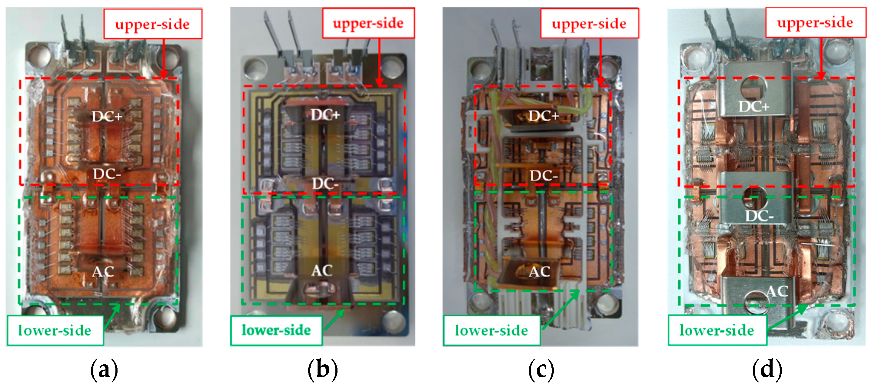
The difference among these modules are mainly reflected in the inner structure and the used power dies including the types and the parallel number of the power dies. As shown in Figure 2, the inner structure of the module_B is same with that of the module_A, but different from that of module_C, while the structure of module_D is different from that of other modules.
As shown in Table 1, there are two types of SiC-MOSFET dies adopted inside the developed modules, the type of adopted SiC-MOSFET dies in module_A is different from that of other modules. The parallel number of SiC-MOSFET dies in module_B is same with that of module_C, and the parallel number of SiC-MOSFET dies in module_D is different from that of module_B and module_C.
With the various designs for the number of parallel-connected power die inside the module, the values of input capacitance of the modules are different accordingly. Thus, the various turn-on speed can be achieved for the modules under the same test conditions (same V D D , I O , and R g e x t ), and with a same gate driver circuit in the following experiments. This is helpful for the study of influence of turn-on speed on the turn-on transient, especially the characteristics of drain-source voltage.
The module_B has the same structure but different power dies with module_A, and also have the same power dies but different structure with module_C. The module_D is designed with only 4 parallel SiC-MOSFET dies and a consequent very small input capacitance to enable a faster turn-on at high current output. It is worth noting that the circuit is carefully designed to eliminate severe negative gate-source voltage spike during the turn-on transient.
In order to slow down appropriately turn-on speed, the additional common source path is introduced in both module_A and module_B, but for other modules, the common source path inside modules is minimized. In addition, since the turn-on speed of module_D is much higher than other modules, in order to avoid the interference due to a faster turn-on speed to the gate-source voltage of the module at turn-on transient, the difference in gate-source routings for the parallel power dies is reduced, and the symmetry of them is improved, meanwhile, the drain-source path inside module is also optimized to reduce its parasitic inductance.
Based on these designs, the influence of power dies on characteristics of v D S can be compared between module_A and module_B, while the influence of module’s structure on characteristics of v D S can be compared between module_B and module_C. The impact of the faster turn-on speed on characteristics of v D S can be reflected from module_D under the same gate driver circuit and test conditions.

2.2. Introduction of the Double Pulse Test Platform

The physical picture of the clamped inductive DPT rig is shown in Figure 3a. The device under test (DUT) is the developed module. The decoupling capacitor is from KEMET. The load inductor is self-fabricated by serial-connected two inductors. The DC bus capacitor with part number of FG810K901-1 is from VDTCAP. The voltage rating of this DC bus capacitor is 900 V. Due to this, we have to ensure that the sum of the applied DC bus voltage ( V D D ) and overshoot voltage is no more than 900 V at experiments.
The 1GHz high definition oscilloscope with part number of HDO6104A used for acquiring the voltage and current signals is from Teledyne Lecroy. A Rogowski current waveform transducer with part number of CWT miniHF 1B utilized to measure drain-source current of DUT is from PEM, the bandwidth of this current probe is 30 MHz. A passive voltage probe with part number of PP026-2 used for measuring gate-source voltage is from Teledyne Lecroy, the bandwidth of this voltage probe is 500 MHz. A high voltage differential probe with part number of HVD3106 used to obtain the drain-source voltage is from Teledyne Lecroy, the bandwidth of this high voltage probe is 120 MHz.
The schematic diagram of the DPT circuit is shown in Figure 3b. The double pulse signal is applied to the gate-source of DUT by gate-driver circuit. The gate-source voltage for turning off and turning on switches is −2.3 V and 17.5 V, respectively. The R g e x t is external resistor of the gate driver circuit. The values of electrical parameter of some components in DPT rig are listed in Table 2.

2.3. Introduction of the Turn-On Transient Process for SiC High-Power Module

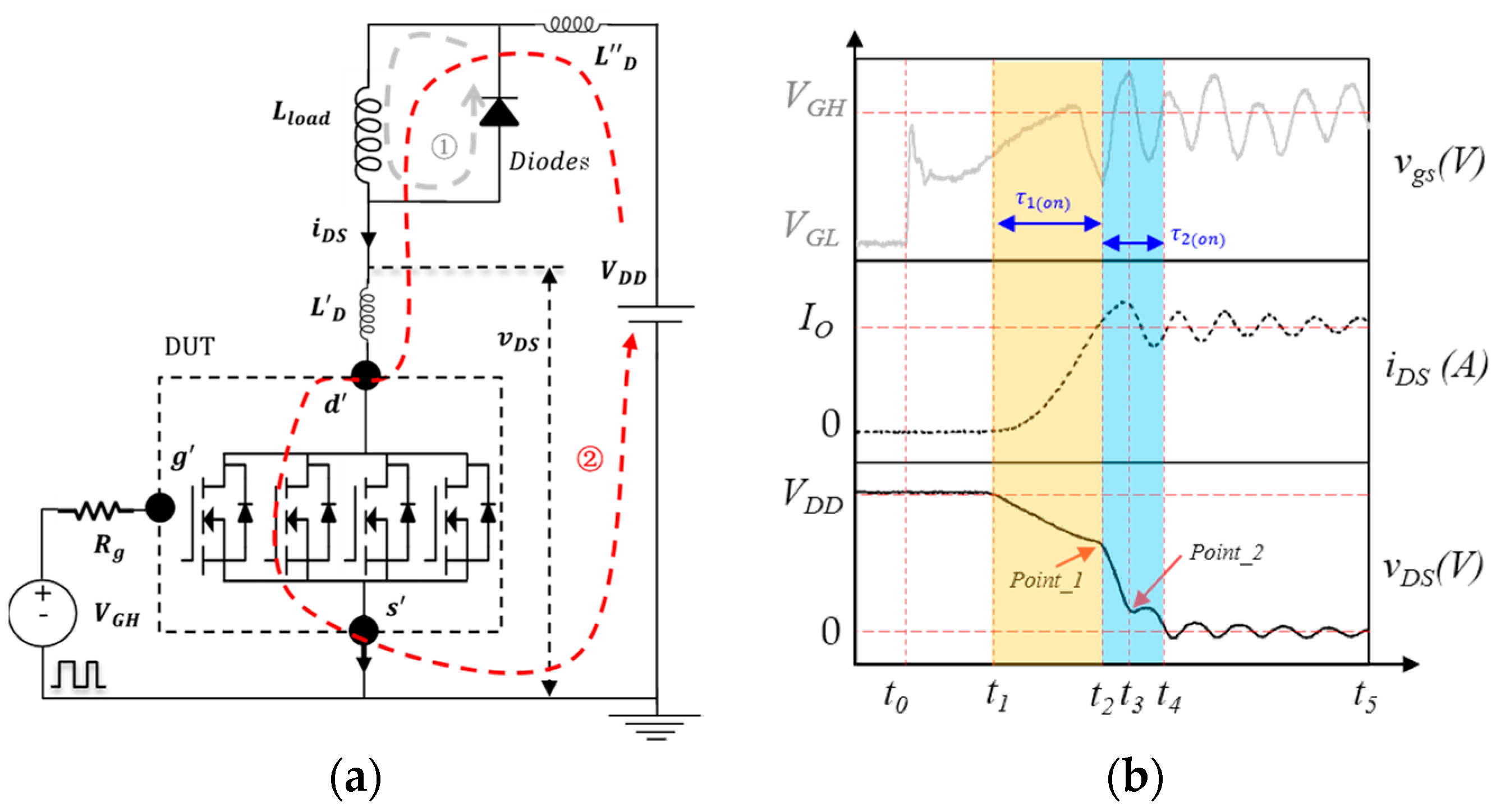
The diagram of commutation paths at turn-on transient is shown in Figure 4a, SiC MOSFET dies are in off-state off initially, the voltage applied between gate and source (VGS) is set to VGL, the load current circulates along the loop_①, as shown by the gray dash line. At turn-on transient the gate-source voltage (VGS) increase from VGL to VGH, the circulating current starts to transfer from the loop_① to the loop_②, as marked by red dash line. After turn-on transient process, the load current flows fully by SiC-MOSFETs, instead of the freewheeling diodes.
The typical diagram of turn-on transient for SiC high-power module is shown in Figure 4b. The whole fall process of v D S at turn-on transient can be divided by two distinct phases.
The phase from t 1 to t 2 is the 1st turn-on interval, τ 1 (on). During the τ 1 ( on ) , with the i D S rises to I O , the v D S fall linearly with time and the v g s is pulled down to a lowest value, due to the negative feedback effect. The voltage drop induced by the rising i D S and parasitic inductance is given by
V D S = L D d i D S d t
where L D is the parasitic inductance of the whole drain circuit loop in DPT, which includes the parasitic inductance of routings from the power terminals of “DC+” to “DC−” inside the module, L D _ 1 , and the parasitic inductance of drain circuit loop excluding the routings inside the module in DPT, L D _ 2 .
The phase from t 2 to t 4 is the reverse recovery process of the freewheeling diodes, which is the 2nd turn-on interval, τ 2 (on). It consists of two sub-phases. During sub-phase from t 2 to t 3 , the i D S continues to rise to its maximum, since the voltage starts to be clamped to freewheeling diode, the v D S reduces in a higher d v D S /dt due to reverse recovery. During the sub-phase from t 3 to t 4 , the reverse recovery current of freewheeling diode decreases from its maximum to zero, the i D S also decreases from the maximum to I O , the turn-on transient of SiC-MOSFET is completed at the end of this phase.
During this phase from t 2 to t 4 , the operation mode of SiC-MOSFET dies changes from saturation region to linear region. After t 4 , the SiC-MOSFET is fully turned-on. All v g s , v D S , i D S characteristics are kept in oscillation state with their respective frequencies which are determined by the parasitic parameters in the circuit.
As shown in Figure 4b, during the v D S falls from V D D to zero, the operation mode of SiC-MOSFET dies changes from saturation region to linear region. Point_1 is the turning point for v D S , changing from τ 1 ( on ) to τ 2 ( on ) during SiC-MOSFET dies operate in saturation region, which corresponds to the moment when i D S rises to I O , while Point_2 is the turning point in v D S when the operation mode of SiC-MOSFET dies changing from saturation to linear region, which corresponds to the moment when i D S rising up to the maximum value.
Under the combined impacts of multiple factors such as various test conditions, turn-on speed and structures of DUT, the turn-on transients of v D S from t 1 to t 4 are probably varied in more than one dimension, the values of the key turning point vary, and, meanwhile, the characteristics of v D S waveforms such as the number of key turning points and the shape of drain-source voltage waveform also change, so that the different characteristics of the falling process of v D S waveforms could be observed. Therefore, in order to facilitate comparison between the modules in the following sections, we neglect the variations in the value of the turning point and just focus on changes in characteristics of v D S , such as the number of key turning points, whether there is a characteristic of point_2 or not, and whether there is a characteristic of the voltage plateau or not.

3. Experimental Results

The turn-on transient of SiC high-power module is essentially the charging process of the input capacitance of the module by the gate driver circuit. The rise of i D S is determined by the charging speed of the input capacitance of the module. We can simply view this system consisting of gate driver and the input capacitance of the module as a one-order low-pass resistance-capacitance (RC) network, where the output of gate driver circuit can be regarded as input signal of the network, and the gate-source voltage ( v g s ) is the output of this network. The response of this network to the turn-on signal determines the ideal transient waveform of v g s and defines the turn-on speed of the module. To facilitate analysis, we use the rise time of this one-order low-pass RC network as a precursor of turn-on speed of the module. Since the module operates in saturation mode, the i D S is proportional to the v g s at turn-on transient. Hence, a shorter rise time means a faster turn-on speed for the developed modules.
The rise time of the output for the one-order low-pass RC network can be given by
t r = 2.2 R g C i s s
where t r is rise time, R g is the resistance of the whole gate driver loop, C i s s is the input capacitance of the module. According to Equation (3), there are two ways to increase the turn-on speed of the developed modules for a specific gate driver circuit, namely, reducing the external gate resistance in DPT and driving a module with a lower input capacitance. Based on the input capacitance of the developed modules shown in Table 1, it is predicted that the turn-on speed of module_A is the slowest, while module_D is the fastest under the same test conditions (same V D D , I O , and R g e x t ).
In order to investigate the influence of module’s structures on the turn-on transient of v D S , the comparative experiments are carried out under various conditions of V D D . Finally, the trend of changes in influence of module’s structures on characteristics of v D S with the increase of tun-on speed or the reduce of V D D is summarized.

3.1. Turn-On Transient at Condition of Relatively High V D D

The experimental results under relatively high V D D are shown in Figure 5, Figure 6 and Figure 7, where V D D is set to be 400 V, I O is set to be 200 A, and R g e x t is set to be 2.4 Ω. The green, red, black, and purple lines stand for the experimental results of module_A, module_B, module_C, and module_D, respectively; the solid and dash lines stand for the experimental results of the upper-side and lower-side respectively for a corresponding module.
Figure 5 shows the comparison of turn-on transient waveforms of module_A and module_B, which have the same structure design but different power dies. The characteristics of v D S are same with each other, the characteristics of v D S of two modules show two turning points, as marked by Point_1 and Point_2 in Figure 5b, though the values of the turning points corresponding to each other show some difference between two modules, such as 28.7 V in upper-side and 30.4 V in lower-side for Point_1.
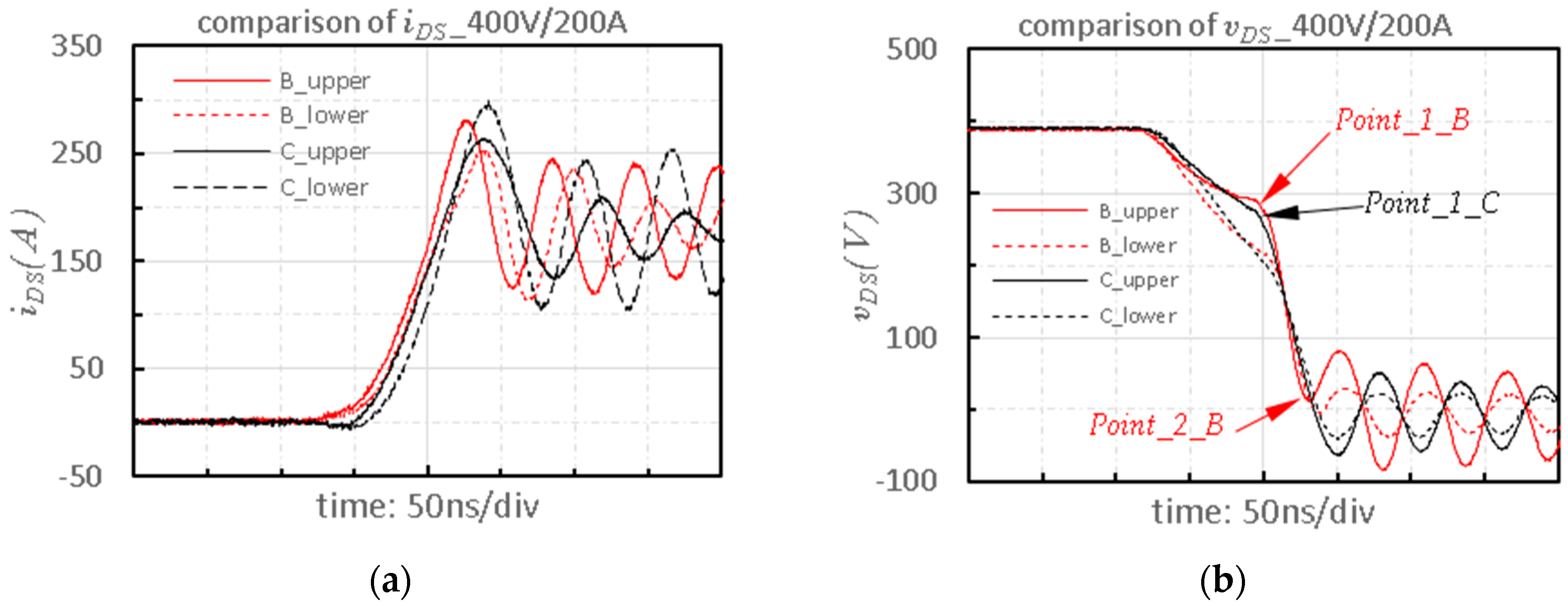
Figure 6 shows the comparison of turn-on transient waveforms of module_B and module_C, which have the same power dies but different structure designs. The characteristics of v D S of module_C is different from that of the module_B, and there is only Point_1 existing in v D S waveform, Point_2 which corresponds to the operation mode of SiC-MOSFET dies changing from saturation to linear region is not observed in v D S , as shown in Figure 6b. In addition, the difference in value of v D S at Point_1 between these two modules still exists but it is reduced, e.g., it is just 16.4 V on the upper-side, while it is 9.6 V on the lower-side.
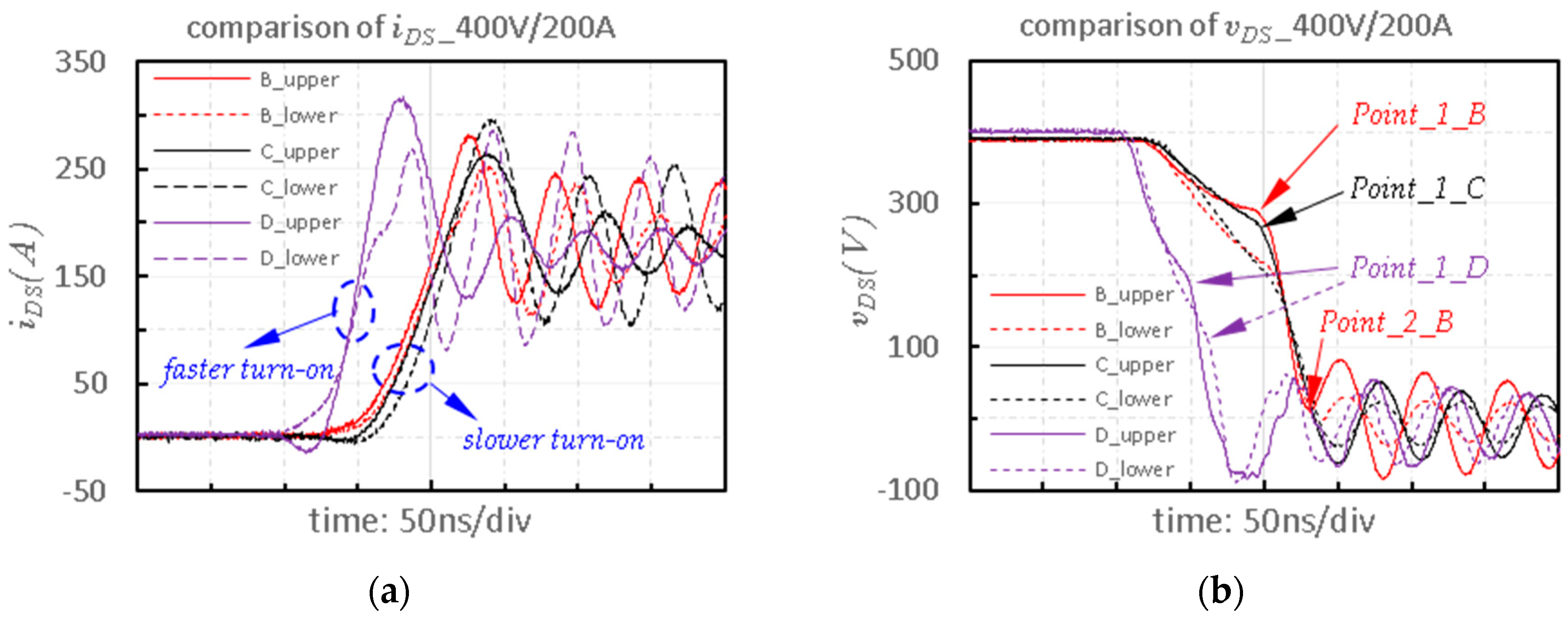
Figure 7 shows the comparison of turn-on transient waveforms of the modules with various turn-on speed. The turning on process of module_D is faster than that of the other modules, due to the smaller input capacitance and shorter rise time, the characteristic of v D S in module_D is fully different from that of other two modules, Point_1 is negligible and Point_2 disappears, as shown in Figure 7b. This means that as turn-on speed increases, the v D S falls faster at turn-on transient, as a result, the characteristics that is corresponding to the operation mode of SiC-MOSFET dies changing from saturation to linear region in τ 2 ( on ) disappear in v D S , and characteristics that is corresponding to the v D S changing from τ 1 ( on ) to τ 2 ( on ) during the SiC-MOSFET dies operating in saturation mode, start to be weakened in v D S .
In summary, although the voltage values of the corresponding Point_1 are different from each other, the characteristics of v D S for the modules with the same structure design are same, and the characteristics of v D S for the modules with the different structure design are different.

3.2. Turn-On Transient at Condition of Low V D D

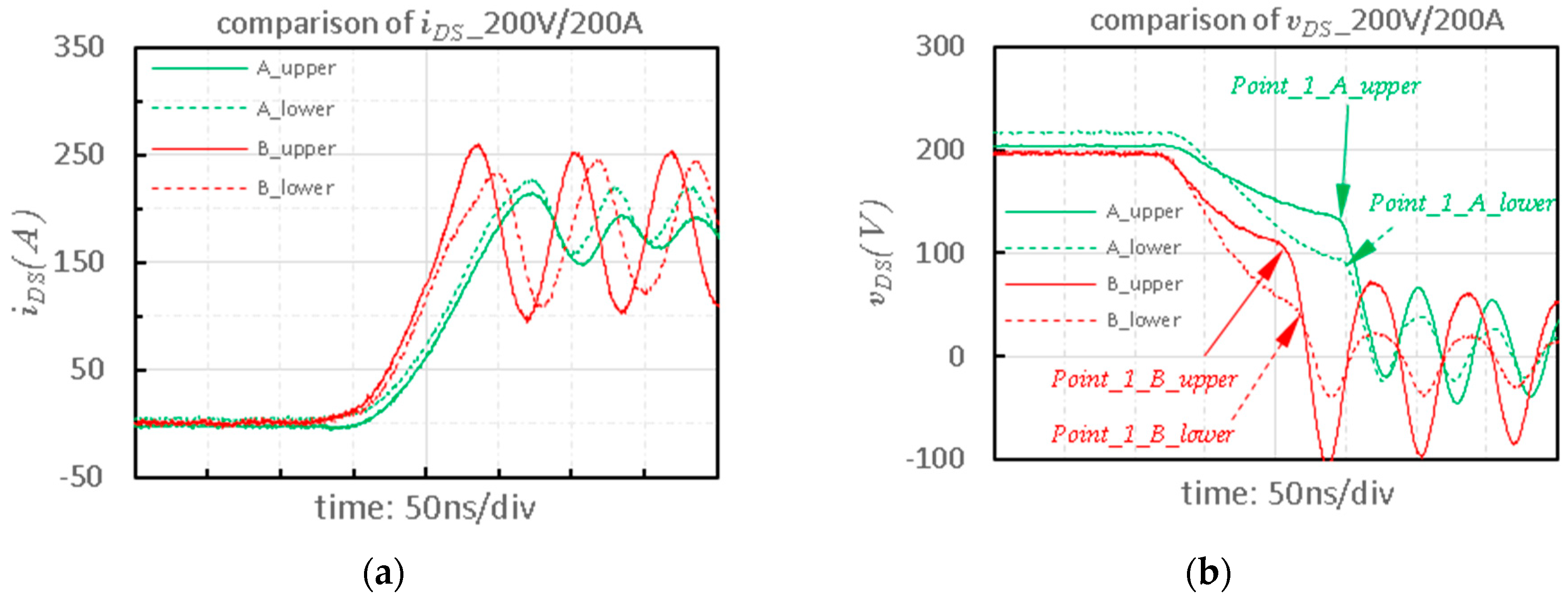
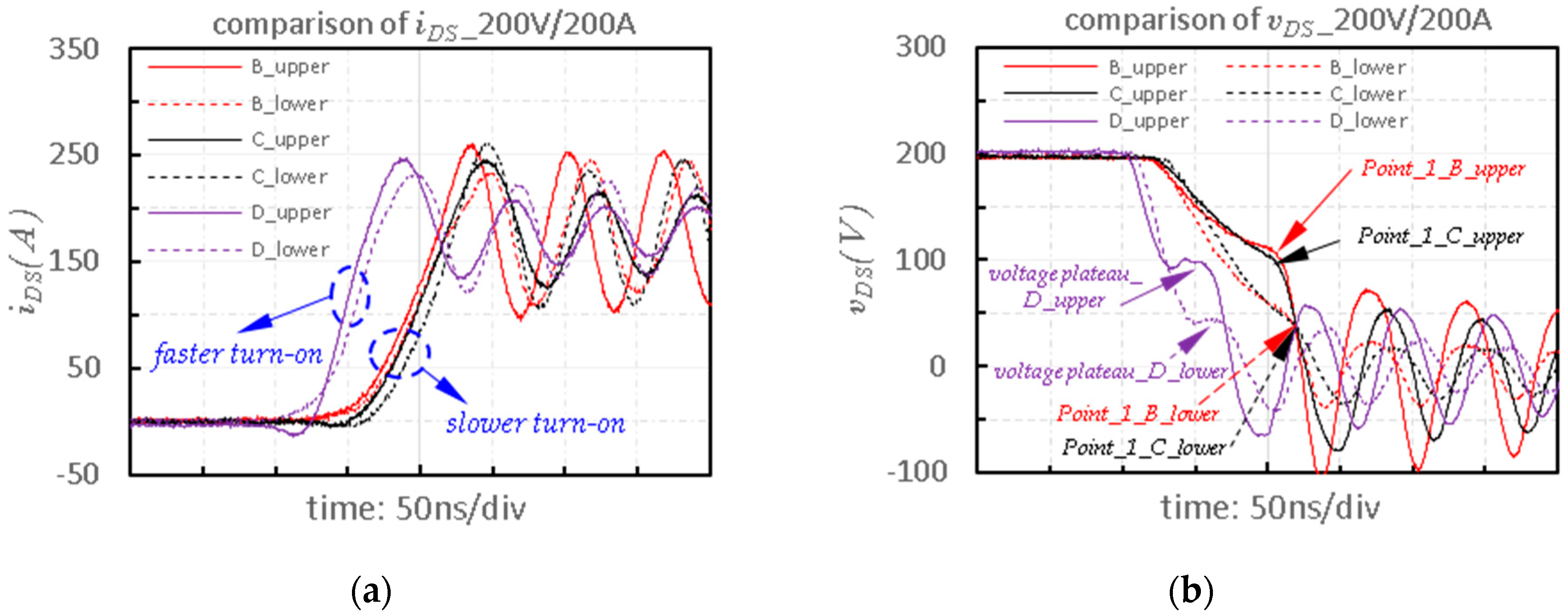
The experimental results under the condition of relatively low V D D are shown in Figure 8 and Figure 9, where V D D is set to be 200 V, I O is set to be 200 A, and R g e x t is set to be 2.4 Ω.
Figure 8 shows the comparison of turn-on transient waveforms of module_A and module_B in low V D D condition, the two modules have the same structure design but different power dies. It is shown that the characteristics of v D S of the two modules are similar, that is, only one turning point is observed. This is different from the case of high V D D condition. The decrease of V D D causes the characteristic corresponding to the operation mode of SiC-MOSFET dies changing from saturation to linear region in τ 2 ( on ) disappears in v D S . As depicted previously, the difference in values of v D S at Point_1 between the two modules still exists. The difference in values of v D S at Point_1 between the two modules is 13.5 V in upper-side and 40.8 V in lower-side.
The characteristics of v D S for the modules with the same structure design are same, though the level of V D D takes effect on characteristics of v D S at turn-on transient and there is a difference in the value of v D S at point_1 between the different modules.
Figure 9 shows the comparison of turn-on transient waveforms of module_B, module_C, and module_D in condition of low V D D . For module_B and module_C, their turn-on speed is relatively slower, the characteristics of v D S is not different from each other, although the module structure design is different. Namely, both modules show only one turning point. The discrepancy in characteristics of v D S caused by the difference of module structures in the case of high V D D condition is not observed in lower V D D case. Hence, the lower V D D weakens the influence of module’s structures on the characteristics of v D S , the difference of module’s structures does not result in the different characteristics of v D S , except for the difference in values of v D S at Point_1 between two modules which is 8.8 V at the upper-side and 2.4 V at the lower-side for Point_1.
However, when the turn-on speed is faster as for module_D, the voltage plateau is observed from the characteristic of v D S for both upper-side and lower-side, also, the value of v D S for the voltage plateau in upper-side is higher than that of lower-side by about 50 V.
Table 3 shows the comparison about characteristics of v D S . Under the condition of relatively high V D D , the characteristics of v D S are greatly affected by the module’s structure. If the module’s structures are same, the characteristics of v D S will be the same, even if the power dies inside the modules are different from each other. On the other hand, if the structures of the modules are different, the characteristics of v D S are deviated from each other even if the used power dies and their parallel number inside the modules both are same. In addition, the faster turn-on speed can further alter the characteristics of v D S , so that the characteristic of Point_1 for v D S changing from τ 1 ( on ) to τ 2 ( on ) become less obvious.
Under the condition of low V D D , the difference of module’s structures does not cause the significant different characteristics of v D S , but the module design with faster turn-on speed causes the distinct characteristics of voltage plateau in v D S between upper-side and lower-side of the module.

3.3. Turn-On Transient at Conditions of a Lower V D D and Various Turn-On Speed

Based on the qualitative comparison and analysis of experimental results shown in Figure 5, Figure 6, Figure 7, Figure 8 and Figure 9, it can be supposed that the characteristics of voltage plateau shown from the v D S waveforms at turn-on transient are due to the combined impacts of fast turn-on speed and low V D D with a specific module structure.
In order to reveal the mechanisms behind the characteristics of the voltage plateau and the impacts of turn-on speed, test conditions and module structure, another experiment is carried out with module_D, in which V D D is fixed at a low value 100 V and the turn-on speed is controlled with three groups of external resistors ( R g e x t ).
Figure 10 shows the comparison of characteristics of v D S among the various turn-on speeds by using different R g e x t . The green, black, and red lines stand for the experimental results under the condition of R g e x t equal to 11 Ω, 5 Ω, and 2.4 Ω, respectively, and the solid and dash lines stand for the upper-side and lower-side, respectively.
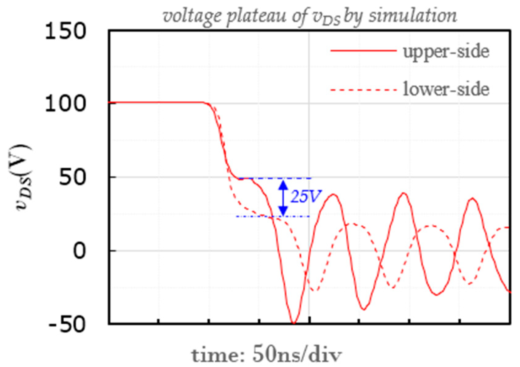
From Figure 10, characteristics of voltage plateau in v D S are observed for the cases of R g e x t equals to 5 Ω and 2.4 Ω, in which the turn-on speed both are faster than 2.64 A/ns (this is turn-on speed of lower-side for the case of R g e x t equals to 5 Ω.), the difference in value of the drain-source voltage plateau between upper-side and lower-side is almost same regardless of the rise of the turn-on speed, which is about 25 V.
In addition, the characteristic of Point_1 is obvious for the case of R g e x t equals to 11 Ω. Compared with the previous characteristics of negligible Point_1 in v D S shown in Figure 7b, it is further confirmed by experiment that the rise of the turn-on speed strengthens the influence of module’s structure on the characteristics of v D S .
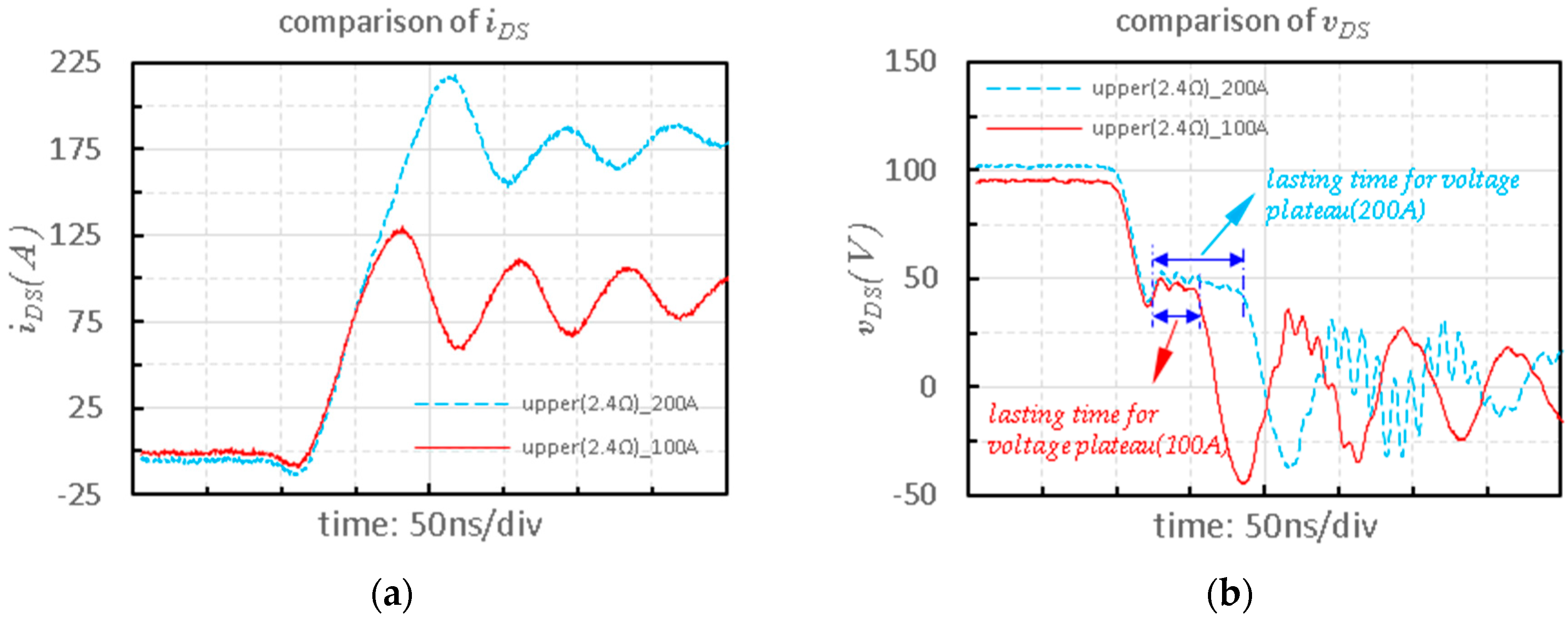
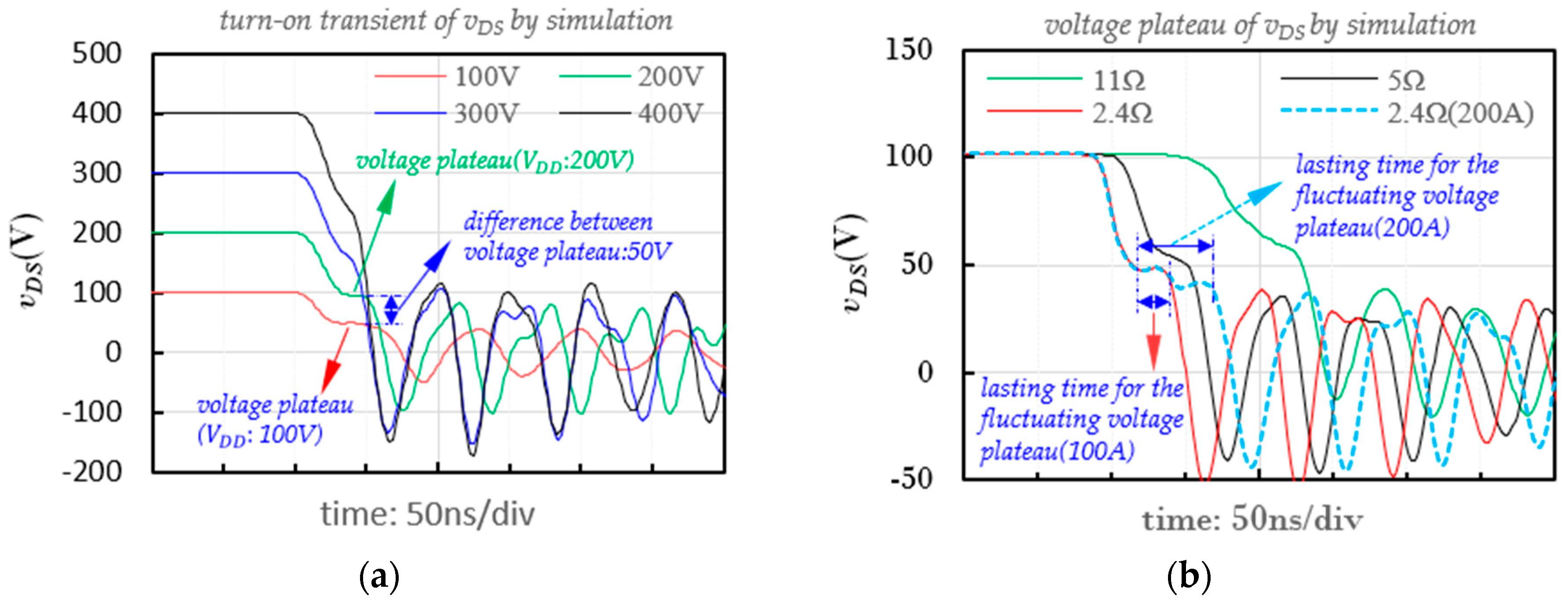
Figure 11 shows that the load current ( I O ) has effect on characteristics of voltage plateau in v D S , where the transient waveforms of the upper-side under the condition where V D D is equal to 100 V, I O is equal to 200 A, and R g e x t is equal to 2.4 Ω (dash lines with the color of light blue) are added together and aligned with time. It is disclosed that the increase in I O just extends the lasting time of the voltage plateau for the characteristics of v D S , it does not change the value of the voltage plateau.
In summary, for SiC high-power modules, the characteristics of v D S are varied under combined conditions of multiple factors, such as the structure of the module, turn-on speed, V D D , and I O . The influence of the module’s structure on the characteristics of v D S is weakened as the V D D reduces, and strengthened as the turn-on speed rises. If the turn-on speed is fast enough (e.g., more than 2.64 A/ns, as shown in previous experiments), under the condition of high V D D , the characteristic of the turning point for v D S changing from τ 1 ( on ) to τ 2 ( on ) during SiC-MOSFET dies operate in saturation region will become negligible, while under condition of low V D D , the characteristic of voltage plateau will be observed in v D S . Furthermore, the distinct characteristics of drain-source voltage plateau between the upper-side and lower-sides of the module are related to the combined impacts of fast turn-on speed and low DC bus voltage, as well as the different structures of the two sides inside the module.

4. Simulation Study for Mechanism of Drain-Source Voltage Plateau

4.1. Mechanism for Characteristic of Drain-Source Voltage Plateau

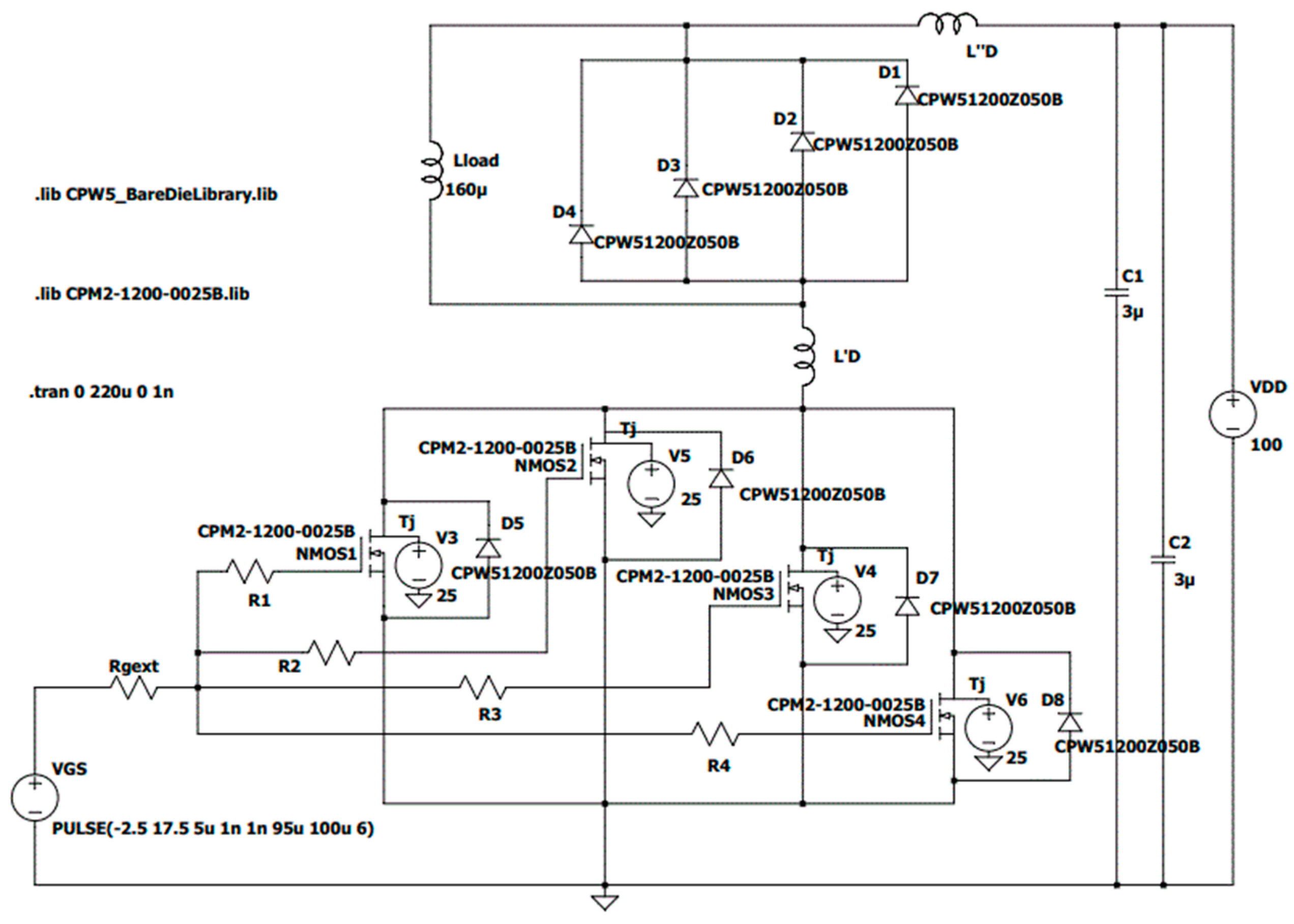
The v D S of module_D at turn-on transient is simulated by LTsipce software. The diagram of the schematic circuit for simulation is shown in Figure 12. The parasitic inductance of drain circuit loop ( L D ) is also divided into two parts, which are L D and L D , respectively. The L D is the parasitic inductance belong to the partial path of drain circuit loop, which is shared with path between two test points for acquiring transient v D S , while L D is the parasitic inductance related to the other part of the drain loop.
The simulation of the influence of the V D D on voltage plateau is conducted based on the upper-side of module_D. In simulation all the parameters and conditions are same with each other, except for the condition of V D D , where V D D is set to be 100 V, 200 V, 300 V, and 400 V, respectively. The value of the parasitic inductance related to the power module and DPT rig are extracted by Q3D software, which are listed in Table 4.
Figure 13a shows that the characteristic of voltage plateau is observed as V D D deceases (<300 V) in simulation. The values of voltage plateau in condition of V D D equals to 200 V and 100 V are about 100 V and 50 V, respectively. These simulation results about characteristics of voltage plateau in v D S are in good agreement with the previous experimental results (Figure 9b and Figure 10b).
Figure 13b shows the simulation about the influence of rise of turn-on speed and I O on characteristics of voltage plateau. The simulation conditions are same with that of experiments shown in Figure 10 and Figure 11. With the rise of turn-on speed, the characteristic of voltage plateau emerges. The characteristic that the increased I O does not change the value of voltage plateau and just increases the lasting time for the voltage plateau, which are also observed in simulation.
These simulation results about the characteristics of v D S in voltage platform agree with the experimental results. There is a little discrepancy of voltage fluctuation over voltage plateau between experiment (see dash line in light blue color in Figure 11b) and simulation (see the dash line in light blue color in Figure 13b). In the actual experiment the v D S is forced into stage of voltage plateau, while the v D S enters slowly stage of voltage plateau in simulation; secondly, the v D S fluctuates over stage of voltage plateau more violently than that of simulations. This is due to the simplification of the simulation model, and some parasitic parameters or effects that may exist in actual experiment have not been considered.
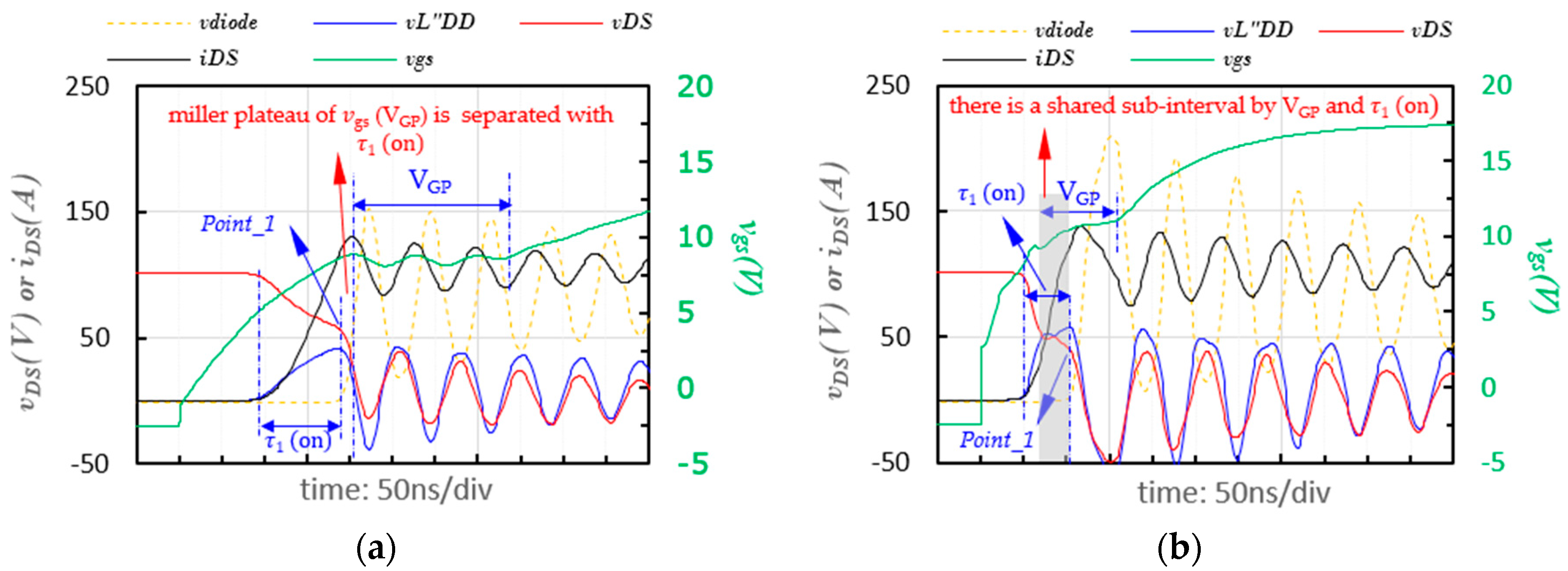
Figure 14 shows that during the interval of τ 1 ( o n ) , the V D D and forward voltage drop of freewheeling diodes ( V F _ d i o d e s ) are shared by L D and L D , and the transient voltage of these two parasitic inductance (which are v L D and v D S , respectively) are dependent on the slew rate of i D S . The relationship is given by
V D D + V F _ d i o d e s = ( L D + L D ) d i D S d t
Before the interval of τ 1 ( o n ) , the i D S does not rise significantly, the v D S is the sum of V D D and V F _ d i o d e s , since the value of V F _ d i o d e s is about 1.3 V and the value of V D D is several hundred volts, the value of v D S is viewed as V D D . During τ 1 ( o n ) , the i DS rises rapidly, the d i DS / d t also rise, accordingly, the voltage over the L D increase, as a result that the v D S falls. After τ 1 ( o n ) , the freewheeling diodes enter the reverse recovery process and start to regain the reverse voltage blocking capability. The voltage is clamped to the freewheeling diodes as shown by the dash line in orange color, accordingly, the v D S shown by the solid-line in red color and the v L D shown by the solid-line in blue color are collapsed.
When the turn-on speed is slow, as shown in Figure 14a, the miller plateau of v g s ( V G P ) appears after τ 1 ( o n ) , there is no any overlap between them. When turn-on speed is fast enough (e.g., more than 2.64 A/ns shown in previous experiments), as shown in Figure 14b, the interval of V G P and τ 1 ( o n ) have a shared sub-interval between them. This shared sub-interval in τ 1 ( o n ) is a result caused by both fast turn-on speed and low V D D .
In order to figure out the effect of this overlap between τ 1 ( o n ) and GP on characteristics of drain-source voltage plateau, the simulation results about the slew rate of i D S are analyzed in detail. Figure 15 shows that the d i D S / d t has a characteristic of plateau in this shared sub-interval by V G P and τ 1 ( o n ) . Since the tiny change in d i D S / d t (just 0.4 A/ns) in this shared sub-interval, the voltage over the inductance of L D changes by about 3.2 V in this shared sub-interval. Compared with the significant drop of v D S in both the initial stage of τ 1 ( o n ) and the whole τ 2 ( o n ) , the falling of v DS in this shared sub-interval is negligible, so that the characteristic of voltage plateau is observed in v D S .
During the shared sub-interval by τ 1 ( o n ) and GP, SiC-MOSFET dies operate in saturation region, where v g s > V T H and v D S > ( v g s V T H ) , the drain-source current of SiC-MOSFET dies is given by
i D S = g f s ( v g s V T H )
where g f s is trans-conductance of SiC-MOSFET dies. Derivate the Equation (4) from time, we can get
d i D S d t = g f s d v g s d t
During the GP interval, the miller capacitance discharges firstly, then charges reversely by gate current, the most of gate current goes through C g d instead of C g s , hence, the voltage of C g s rise so slowly and voltage plateau appears in v g s , so that the d v g s / d t varies little.
According to Equation (5), the d i D S / d t is determined by d v g s / d t during the shared sub-interval by τ 1 ( o n ) and GP, therefore, the d i D S / d t changes little and appear the characteristic of voltage plateau in v D S .
After the moment corresponding to Point_1, the freewheeling diodes enter the reverse recovery process and start to regain the reverse voltage blocking capability. Consequently, the voltage is clamped to the freewheeling diodes, so that the effect of V G P on the d i D S / d t is not reflected on v D S , therefore, the characteristics of drain-source voltage plateau will end at the moment when i D S rises to I O . However, if the I O increases, this shared sub-interval will be extended, accordingly, the characteristics of voltage plateau in v D S will also be prolonged.
As shown in Figure 15b, when approaching to the end of interval τ 1 ( o n ) , with the change of d i D S / d t rises, the rise in voltage over L D results in the voltage over L D reduces, as a result that the characteristic of Point_1 is weakened.
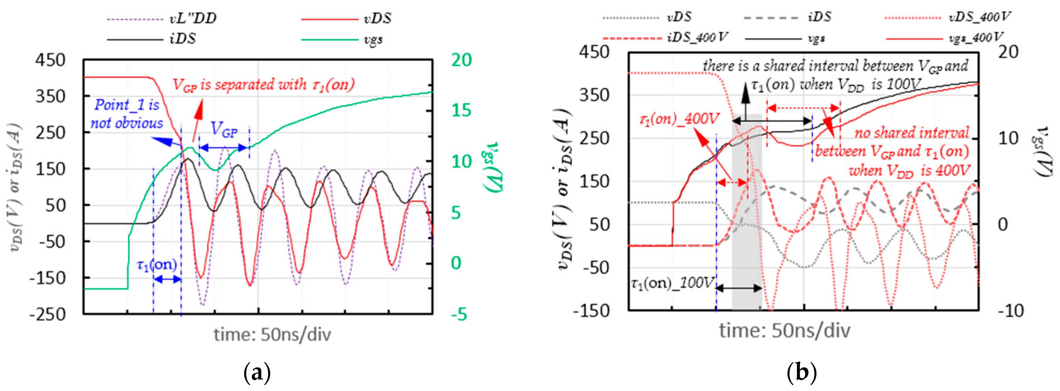
Figure 16 shows the simulation results about the influence of the increased V D D on characteristics of voltage plateau in v D S , where V D D is set to be 400 V, R g e x t is set to be 2.4 Ω, and I O is set to be 100 A. The increased V D D generates the higher d i D S / d t over the L D during the conduction of freewheeling diodes, the freewheeling current in loop_① transfer faster to loop_②, on the other hand, the increased V D D accelerates the turn-on, due to the smaller input parasitic capacitance under high v D S , the v g s can rise to a higher voltage then falls to miller plateau, this higher v g s cause the current of SiC-MOSFETs rises in a higher speed. As shown in Figure 16b, the τ 1 ( o n ) is shortened and V G P is delayed, so that the interval of V G P is separated with τ 1 ( o n ) . As a result, the effect of miller plateau of v g s on d i D S / d t is not reflected in characteristics of v D S , the characteristics of voltage plateau is not developed in v D S , furthermore, the characteristic of Point_1 becomes less obvious.

4.2. Mechanism for Difference of Drain-Source Voltage Plateau between Upper-Side and Lower-Side

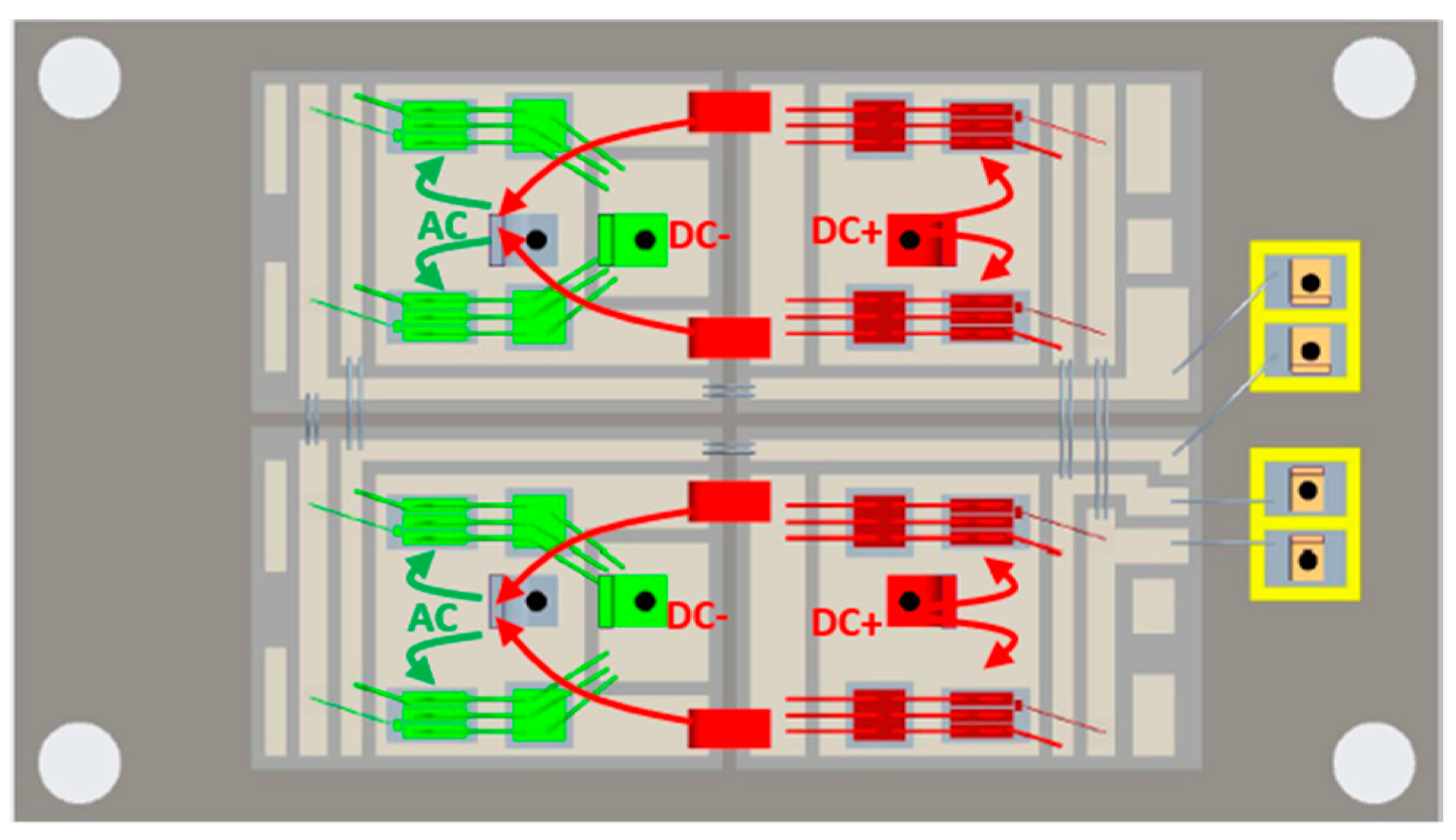
The previous experimental results show us that the measured v D S in voltage plateau for the upper-side is higher than that of lower-side by 50 V in V D D of 200 V, and 25 V in V D D of 100 V. This difference is related to the distinct parasitic inductance in measuring the v D S . The physical outline and locations of power terminals for the developed module are fixed as shown in Figure 1. When measuring the v D S of upper-side the test probe is connected to the power terminals of “DC+” and “AC”, while, when measuring the v D S of the lower-side, the probe is connected to the terminals of “AC” and “DC-“ in the DPT experiment.
Figure 17 illustrates the design of inner routings of the developed module_D, the red-color indicated routings from terminal of “DC+” to terminal of “AC” and the related DBC (direct bonding copper) form the path of upper-side, while the green-color indicated routings from terminal of “AC” to terminal of “DC-“ and the related DBC form the path of lower-side when measuring v D S . The path of upper-side is significantly different from the one of the lower-side inside the module when measuring v D S .
The path of drain circuit loop inside module_D consists of the routings from terminal of “DC+” to terminal of “DC−” and the related DBC. It is obvious that the partial path of drain circuit loop shared with the path of upper-side is different from the one shared with the path of lower-side inside the module. The parasitic inductance of these shared paths between upper-side and lower-side are also different from each other, which is denoted by the L D _ u p p e r and L D _ l o w e r , respectively. The value of the L D _ u p p e r and L D _ l o w e r , were extracted by Q3D software, as shown in Table 4, in which the value of L D _ u p p e r is higher than that of L D _ l o w e r .
Based on the circuit schematic shown in Figure 12 and the distinct L D which is the L D _ u p p e r for upper-side and L D _ l o w e r for lower-side, the turn-on transient waveforms of v D S for module_D are simulated by LTspice under the condition that the V D D is set to be 100 V, the I O is set to be 100 A, and the R g e x t is set to be 2.4 Ω. The other parameters for simulation are the same as that of the experiments shown in Figure 10 and Table 2, as well as Table 4.
Figure 18 shows the simulation result about the difference of characteristics of drain-source voltage between upper-side and lower-side caused by the special structure of the module. The characteristics of voltage plateau in v D S are observed in both the upper-side and lower-side. The simulation results about the difference in the values of drain-source voltage plateau between the upper-side and lower-side is very near to the experimental result of 25 V shown in Figure 10b.
Though the voltage plateau of v D S in the lower-side is not as flat as that of the upper-side and has a slow downward trend, there is difference of characteristics of v D S in the lower-side between experiment and simulation. We can see the similar characteristic in previous experiment shown in dash line in black color for lower-side under condition of R g e x t equals to 5 Ω in Figure 10b. Therefore, the characteristic of voltage plateau in v D S for the lower-side in simulation is normal, while the discrepancy in voltage plateau characteristic for v D S of the lower-side between the experiment and simulation is probably attributed to the difference of test conditions caused by the simplification of the simulation.
In summary, the experimental results are confirmed by simulation that the combined impacts of fast turn-on speed and low V D D causes characteristic of voltage plateau in v D S at turn-on transient. Moreover, the special structure design of the developed module with the standard 62 mm package outline between upper-side and lower-side lead to different characteristics of characteristic of voltage plateau in v D S of each other. The characteristic that the rise of I O does not change the value of voltage plateau and just prolongs the voltage plateau is also confirmed by simulation.
The voltage plateau happens at different v D S values for the upper-side and lower-side, which is verified by simulation. The difference is attributed to the discrepancy of structure in the corresponding partial path of drain circuit loop inside SiC high-power module with the standard 62 mm package outline when measuring v D S of upper-side and lower-side.

5. Conclusions

In this work, the characteristics of drain-source voltage at turn-on transient for the fabricated SiC high power modules are investigated under various test conditions (i.e., various DC bus voltages and turn-on speeds), and the characteristic of the drain-source voltage plateau is observed under the combined condition of fast turn-on speed and low DC bus voltage. The mechanisms behind the voltage plateau characteristics are studied via experiments and simulations.
Under the condition of fast turn-on speed and low DC bus voltage, there is a shared sub-interval by the interval of miller plateau for gate-source voltage and the interval of τ 1 ( o n ) for drain-source voltage, the effect of miller plateau of gate-source voltage on d i D S / d t can be reflected in the characteristics of the drain-source voltage, so that the characteristic of the voltage plateau is generated in the drain-source voltage during τ 1 ( o n ) . After τ 1 ( o n ) , the voltage is clamped to the freewheeling diodes, the v D S falls dramatically, the characteristic of voltage plateau in drain-source voltage disappears. In addition, with the load current ( I O ) increases, the shared sub-interval is prolonged, accordingly, the lasting time for the characteristics of voltage plateau in drain-source voltage is also increased.
When the turn-on speed is slow, the miller plateau of gate-source voltage ( V G P ) appears after τ 1 ( o n ) , there is no any overlap between them. The effect of miller plateau of gate-source voltage on d i D S / d t is not reflected on the characteristics of drain-source voltage, therefore, the characteristics of the voltage plateau are not developed in the drain-source voltage.
When the DC bus voltage is high, the increased V D D shortens the interval of τ 1 ( o n ) and delays the interval for the miller plateau of gate-source voltage, so that the interval for the miller plateau of gate-source voltage is separated with τ 1 ( o n ) , as a result that the characteristic of voltage plateau is not developed in drain-source voltage.
In summary, the experimental results are confirmed by simulation that the combined impacts of fast turn-on speed and low DC bus voltage causes the characteristic of voltage plateau in the drain-source voltage at the turn-on transient. Moreover, the different structure designs of the developed module with the standard 62 mm package outline between the upper-side and lower-side lead to different values of v D S from each other in the voltage plateau.

Author Contributions

Conceptualization, M.Z.; funding acquisition, Q.G. and K.S.; project administration, Q.G.; supervision, K.S.; writing—original draft, M.Z.; writing—review and editing, M.Z., and N.R.; All authors have read and agreed to the published version of the manuscript.

Funding

This research was supported in part by the National Key Research and Development Program of China under Grant 2018YFB0905700, and in part by the National Natural Science Foundation of China under Grant 51777187 and U1766222.

Conflicts of Interest

The authors declare no conflict of interest.

References

  1. Xiao, Y.; Shah, H.; Chow, T.P.; Gutmann, R.J. Analytical modeling and experimental evaluation of interconnect parasitic inductance on MOSFET switching characteristics. In Proceedings of the 19th annual IEEE Applied Power Electronics Conference and Exposition, Anaheim, CA, USA, 22–26 February 2004; Volume 1, pp. 516–521. [Google Scholar]
  2. Teulings, W.; Schanen, J.L.; Roudet, J. MOSFET switching behavior under influence of PCB stray inductance. In Proceedings of the 1996 IEEE Industry Applications Conference Thirty-First IAS Annual Meeting, San Diego, CA, USA, 6–10 October 1996; Volume 3, pp. 1449–1453. [Google Scholar]
  3. Chen, Z.; Boroyevich, D.; Burgos, R. Experimental parametric study of the parasitic inductance influence on MOSFET switching characteristics. In Proceedings of the 2010 International Power Electronics Conference (ECCE ASIA), Sapporo, Japan, 21–24 June 2010; pp. 164–169. [Google Scholar]
  4. Merienne, F.; Roudet, J.; Schanen, J.L. Switching disturbance due to source inductance for a power MOSFET: Analysis and solutions. In Proceedings of the 1996 IEEE Power Electronics Specialists Conference, Baveno, Italy, 23–27 June 1996; Volume 2, pp. 1743–1747. [Google Scholar]
  5. Tiwari, S.; Midtgård, O.-M.; Undeland, T.M.; Lund, R. Parasitic capacitances and inductances hindering utilization of the fast switching potential of SiC power modules. Simulation model verified by experiment. In Proceedings of the 2017 19th European Conference on Power Electronics and Applications (EPE’17 ECCE Europe), Warsaw, Poland, 11–14 September 2017; pp. P.1–P.10. [Google Scholar]
  6. Wang, J.; Chung, H.S.; Li, R.T. Characterization and experimental assessment of the effects of parasitic elements on the MOSFET switching performance. IEEE Trans. Power Electron. 2013, 28, 573–590. [Google Scholar] [CrossRef]
  7. Incau, B.I.; Trintis, I.; Munk-Nielsen, S. Switching speed limitations of high power IGBT modules. In Proceedings of the 2015 17th European Conference on Power Electronics and Applications (EPE’15 ECCE-Europe), Geneva, Switzerland, 8–10 September 2015; pp. 1–8. [Google Scholar]
  8. Zhu, H.; Hefner, A.R.; Lai, J.S. Characterization of power electronics system interconnect parasitics using time domain reflectomentry. IEEE Trans. Power Electron. 1999, 14, 622–628. [Google Scholar]
  9. Dalal, D.N.; Christensen, N.; Jørgensen, A.B.; Jørgensen, J.K.; Bęczkowski, S.; Munk-Nielsen, S. Impact of power module parasitic capacitances on medium-voltage SiC MOSFETs switching transients. IEEE J. Emerg. Sel. Top. Power Electron. 2020, 8, 298–310. [Google Scholar] [CrossRef]
  10. Huang, X.; Ji, S.; Palmer, J.; Zhang, L.; Tolbert, L.M.; Wang, F. Parasitic Capacitors’ Impact on Switching Performance in a 10 kV SiC MOSFET Based Converter. In Proceedings of the 6th IEEE Workshop on Wide Bandgap Power Devices and Applications (WiPDA), Atlanta, GA, USA, 31 October–2 November 2018; pp. 311–318. [Google Scholar]
  11. Ji, S.; Zheng, S.; Wang, F.; Tolbert, L.M. Temperature-dependent characterization, modeling and switching speed limitation analysis of latest generation 10 kV SiC MOSFET. IEEE Trans. Power Electron. 2018, 33, 4317–4326. [Google Scholar] [CrossRef]
  12. Zhang, Z.; Wang, F.; Tolbert, L.M.; Blalock, B.J.; Costinett, D.J. Evaluation of switching performance of SiC devices in PWM inverter fed induction motor drives. IEEE Trans. Power Electron. 2015, 30, 5701–5711. [Google Scholar] [CrossRef]
  13. Fuentes, C.D.; Kouro, S.; Bernet, S. Comparison of 1700-V SiC-MOSFET and Si-IGBT modules under identical test setup conditions. IEEE Trans. Ind. Appl. 2019, 55, 7765–7775. [Google Scholar] [CrossRef]
  14. Zhang, Z.; Zhang, W.; Wang, F.; Tolbert, L.M.; Blalock, B.J. Analysis of the switching speed limitation of wide band-gap devices in a phase-leg configuration. In Proceedings of the 2012 IEEE Energy Conversion Congress and Exposition (ECCE), Raleigh, NC, USA, 15–20 September 2012; pp. 3950–3955. [Google Scholar]
  15. Zhang, M.; Ren, N.; Guo, Q.; Zhu, X.; Zhang, J.; Sheng, K. Modeling and analysis of vgs characteristics for upper-side and lower-side switches at turn-on transients for a 1200V/200A full-SiC power module. Micromachines 2020, 11, 5. [Google Scholar] [CrossRef] [PubMed] [Green Version]
  16. Khanna, R.; Amrhein, A.; Stanchina, W.; Reed, G.; Mao, Z. An analytical model for evaluating the influence of device parasitics on Cdv/dt induced false turn-on in SiC MOSFETs. In Proceedings of the 28th Annual IEEE Applied Power Electronics Conference and Exposition (APEC), Long Beach, CA, USA, 17–21 March 2013; pp. 518–525. [Google Scholar]
  17. Zhang, Z.; Wang, F.; Tolbert, L.M.; Blalock, B.J. Active gate driver for crosstalk suppression of SiC devices in a phase-leg configuration. IEEE Trans. Power Electron. 2014, 29, 1986–1997. [Google Scholar] [CrossRef]
  18. Xu, S.; Sun, W.; Sun, D. Analysis and design optimization of brushless DC motor’s driving circuit considering the Cdv/dt induced effect. In Proceedings of the 2010 IEEE Energy Conversion Congress and Exposition, Atlanta, GA, USA, 12–16 September 2010; pp. 2091–2095. [Google Scholar]
  19. Burra, R.K.; Mazumder, S.K.; Huang, R. DV/DT related spurious gate turn-on of bidirectional switches in a high-frequency cycloconverter. IEEE Trans. Power Electron. 2005, 20, 1237–1243. [Google Scholar] [CrossRef]
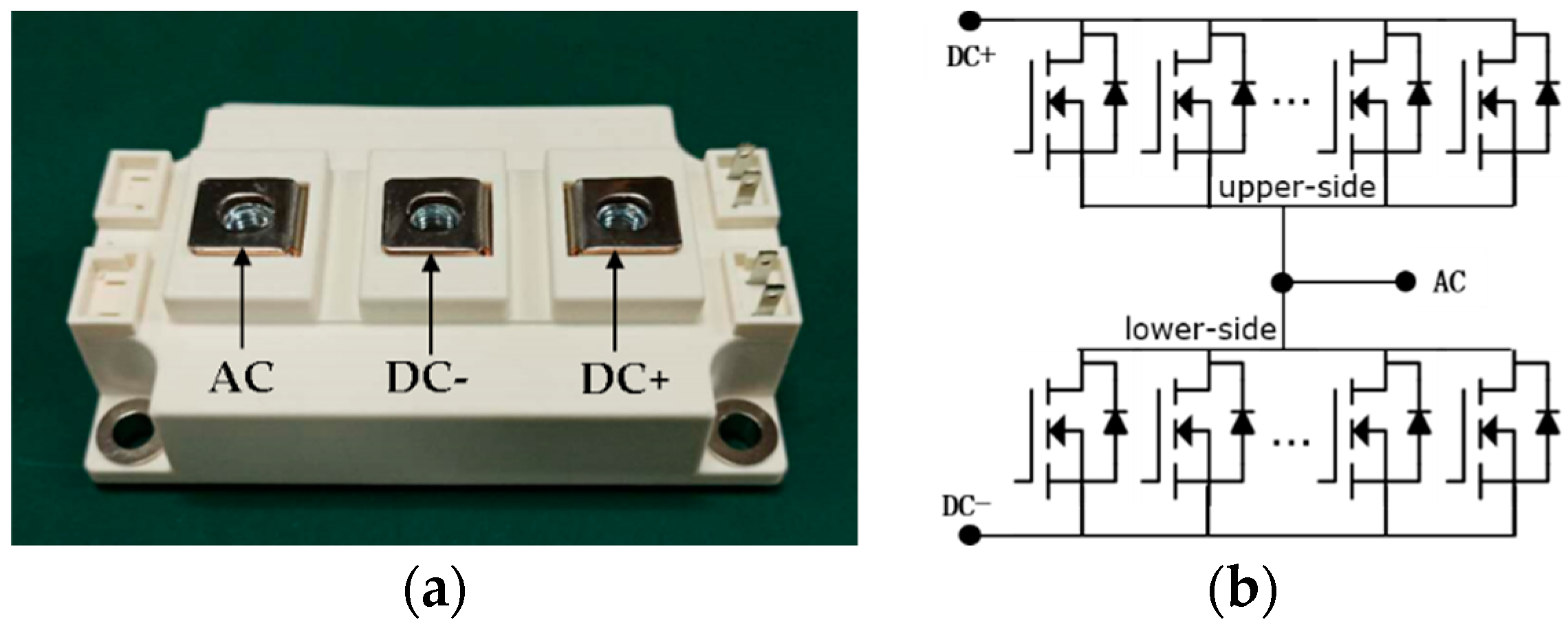
Figure 1. Outline and circuit topology of the developed silicon carbide (SiC) high-power module: (a) standard 62 mm package outline, (b) circuit topology of half-bridge configuration.
Energies 13 03802 g001
Figure 2. The inner structure inside the developed SiC power modules: (a) module_A, (b) module_B, (c) module_C, (d) module_D.
Energies 13 03802 g002
Figure 3. The inductive load double pulse test (DPT) circuit platform: (a) physical picture, (b) schematic diagram of circuit.
Energies 13 03802 g003
Figure 4. Typical diagrams for turn-on transient analysis for SiC high-power module in DPT: (a) commutation paths of the current flow, (b) turn-on transient process.
Energies 13 03802 g004
Figure 5. The comparison of turn-on transient waveforms of the modules with the same structure design but different power dies under condition of high V D D : (a) waveform of i D S , (b) waveform of v D S .
Energies 13 03802 g005
Figure 6. Comparison of turn-on transient waveforms of the modules with different structure design but same power dies under condition of high V D D : (a) waveform of i D S , (b) waveform of v D S .
Energies 13 03802 g006
Figure 7. The turn-on transient waveforms of SiC high-power modules under condition of high V D D : (a) waveform of i D S , (b) waveform of v D S .
Energies 13 03802 g007
Figure 8. The turn-on transient waveforms of the modules with the same structure design but different power dies under condition of low V D D : (a) waveform of i D S , (b) waveform of v D S .
Energies 13 03802 g008
Figure 9. The turn-on transient waveforms of SiC high-power modules under condition of low V D D : (a) waveform of i D S , (b) waveform of v D S .
Energies 13 03802 g009
Figure 10. The comparison of turn-on transient waveforms of the module_D among various turn-on speeds under condition of a lower V D D : (a) waveform of i D S , (b) waveform of v D S .
Energies 13 03802 g010
Figure 11. The comparison of turn-on transient waveforms of the module_D with an increased I O under V D D of 100 V: (a) waveform of i D S , (b) waveform of v D S .
Energies 13 03802 g011
Figure 12. The diagram of schematic circuit for simulation by LTspice.
Energies 13 03802 g012
Figure 13. The simulation results about voltage plateau of v D S for module_D by LTspice: (a) influence of V D D , (b) influence of turn-on speed.
Energies 13 03802 g013
Figure 14. The simulation results about relationship between the τ 1 ( o n ) of v D S and miller plateau of v g s under 100 V/100 A: (a) turn-on sped is slow ( R g e x t = 11   Ω ) , (b) turn-on speed is fast ( R g e x t = 2.4   Ω ).
Energies 13 03802 g014
Figure 15. The simulation results about mechanism of drain-source voltage plateau under 100 V/100 A: (a) plateau d i D S / d t , (b) comparison of v L D and v D S .
Energies 13 03802 g015
Figure 16. The simulation results about the influence of the increased V D D on characteristics of drain-source voltage plateau: (a) voltage waveforms under condition of 400 V/100 A, (b) comparison between V D D of 400 V (in red color) and 100 V (in black color).
Energies 13 03802 g016
Figure 17. Design of routings inside in module_D (red lines for upper-side; green line for lower-side).
Energies 13 03802 g017
Figure 18. The simulation results about difference of drain-source voltage plateau between upper-side and lower-side by LTspice.
Energies 13 03802 g018
Table 1. The used SiC dies inside the developed power module.
Modules 1Module_AModule_BModue_CModule_D
SiC-MOSFET diesS2301TCSTCPM2-1200-0025BCPM2-1200-0025BCPM2-1200-0025B
Parallel number of dies12884
Supplier of diesROHMCREECREECREE
Input capacitance24.12 nF22.30 nF22.30 nF12.15 nF
Voltage/Current ratings1200 V/300 A1200 V/400 A1200 V/400 A1200 V/200 A
1 Note: There are anti-parallel SiC-SBD dies as freewheeling diodes in the module_D, which is the CPW5-1200-Z050B from CREE, its parallel number is 4. There are no anti-parallel diodes used in the other modules.
Table 2. The value of electrical parameter of components in DPT rig.
ComponentsNamesValue
DC-bus capacitorC11000 μF
Decoupling capacitorC23 μF
Decoupling capacitorC33 μF
Load inductor L l o a d 160 μH
Table 3. The comparison about characteristics of v D S over number of turning points.
Number of Turning PointsModule_AModule_BModule_CModule_D
High V D D 2211
Low V D D 1111 1
1 There are characteristics of drain-source voltage plateau observed in module_D.
Table 4. Summary of the parasitic element of modules and DPT.
Parasitic Inductance of Paths or RoutingsSymbolUpper-SideLower-Side
Routings from terminals of DC+ and DC- inside module L D 1 (nH)16.4616.46
Paths of drain circuit loop outside module in DPT L D 2 (nH)12.5612.56
Common part of the routings, L D _ u p p e r and L D _ l o w e r L D (nH)7.955.14