Article

Research on the Equivalent Virtual Space Vector Modulation Output of Diode Clamped N-level Converter under Multi-Modulation Carrier Modulation

1
Department of Electrical Engineering, Xi’an Jiaotong University, Xi’an 710049, China
2
Department of Energy, Aalborg University, DK-9220 Aalborg, Denmark
*
Author to whom correspondence should be addressed.
Energies 2020, 13(15), 3803; https://doi.org/10.3390/en13153803
Submission received: 9 July 2020 / Revised: 16 July 2020 / Accepted: 22 July 2020 / Published: 24 July 2020

Abstract

:
Diode-clamped multi-level converters have DC-side capacitors in series, which will lead to the unbalance of DC-side capacitor voltage, the distortion of the output waveform, the increase of total harmonic distortion (THD), and even the damage of switching devices, which will make the system inoperable. The proposal of virtual space vector pulse-width modulation (VSVPWM) realizes the balanced control of the capacitor voltage, but when the output level of converter increases, the implementation of VSVPWM becomes very complicated, and the amount of calculation also increases greatly, thus hindering its application in the multi-level circuit. Compared with VSVPWM, the carrier-based pulse-width modulation (CBPWM) is simple to operate and easy to implement. If the equivalent relationship between CBPWM and VSVPWM can be found, the application of VSVPWM can be generalized to any level, and the advantages of VSVPWM can be fully utilized. This paper aims to study the inner relationship of VSVPWM and the multi-modulation carrier CBPWM (MCBPWM). After strict theoretical analysis, the equivalent relationship of VSVPWM and MCBPWM in the three-level and four-level and converter is realized by injecting the zero-sequence component into the modulation waves. Furthermore, the equivalent relationship between VSVPWM and MCBPWM is deduced to the N-level converter. Finally, the correctness of the relevant theoretical analysis is verified by the experiment.

Graphical Abstract

1. Introduction

In recent years, the diode-clamped multi-level converter has been widely used in many fields due to its low switching stress and low harmonic distortion rates [1], such as power system DC transmission [2], reactive power compensation [3], active power filter and frequency conversion speed regulation of high-voltage high-power AC motor, etc. However, because the DC side capacitors of the converter are connected in series, the DC side voltage will be unbalanced [4]. Virtual space vector pulse-width modulation (VSVPWM) was first proposed for the capacitor voltage balance of three-level neutral-point-clamped (NPC) converters [5]. Through VSVPWM, the neutral current of the DC side is zero during the switching cycle, and the voltage of the capacitor can be well balanced within the range of full modulation and load power factor [6,7,8]. However, when the levels of diode-clamped multi-level converters increase, the implementation of VSVPWM is very complicated, and the amount of calculation will greatly increase, hindering its application in multi-level circuits. Therefore, VSVPWM is mainly used in three-level converter and when the level of the converter is greater than three levels, VSVPWM is rarely used. Compared with VSVPWM, the carrier-based pulse-width modulation (CBPWM) method appears earlier, it is easy to operate and implement [9,10], which is convenient for use in multi-level converters with greater than five levels, the theoretical and practical research has been relatively mature and widely used in practice. If the equivalent relationship between CBPWM and VSVPWM can be found, the modulation effect of VSVPWM can be realized by a simple and easy-to-implement CBPWM method, the application of VSVPWM can be extended to any level, and the advantages of VSVPWM can be fully utilized.
Reference [10] first proposed the three-phase three-level VSVPWM to realize the inverter neutral line non-current. In references [11,12], the realization of four-level and five-level VSVPWM are mainly deduced based on three-level. It is not difficult to find that with the increase of levels, the VSVPWM becomes particularly complex and difficult to be applied in higher-level situations. In references [13,14], the equivalent relationship between the CBPWM and SVPWM modulation strategies is preliminarily analyzed, and the three-level eight-segment modulation sequence is derived. By injecting a zero-sequence voltage into each phase modulation voltage under CBPWM, the modulation effect of the two is equivalent. However, this method is limited to eight-segment modulation, and the output level of each phase can only be two levels. Reference [15] achieves the equivalent relationship between space vector pulse-width modulation (SVPWM) and CBPWM of single-phase three-level NPC converters by injecting offset voltage, however, it only studies the single-phase three-level converter and there is no study on three-phase or higher-level converters. Reference [16] proposed a brand-new modulation wave decomposition strategy, which makes the decomposition of more than eight-segment space vector output sequences possible, perfecting the realization of the equivalent relationship. However, it only studies a three-level converter and does not study higher-level output converters. Reference [17] studies an equivalent relationship between SVPWM and CBPWM of the n-level converter, it assumes the DC side voltage of the converter is constant and does not consider the unbalance of DC side capacitors. Therefore, there is no modulation strategy used to solve the neutral current generated by the voltage vector. References [18,19] analyzed the three-phase three-level virtual space vectors. By solving the volt-second balance and the boundary condition equations, the equivalence between the three-phase dual-modulated wave CBPWM and VSVPWM 10-segment sequences was realized. However, it does not study how the command voltage modulated wave is decomposed into double modulated waves and does not give the expression of the zero-sequence component of the equivalent relationship. Moreover, the equivalent relationship between VSVPWM and CBPWM above three levels has not been studied. In addition, as the number of levels increases, the number and difficulty of solving equations will greatly increase, which is not conducive to promotion to multiple levels. Therefore, through the analysis of domestic and foreign references, there is no reference to study the equivalent relationship between CBPWM and VSVPWM of NPC multi-level converter with arbitrary output levels. Once the equivalent relationship of two is found, the equivalent output of VSVPWM can be realized by CBPWM, which can not only simplify the complex calculation but is also easy to implement in higher-level converters with low switching stress and low harmonic distortion rates.
In this paper, the relationship between VSVPWM and multi-modulation carrier CBPWM (MCBPWM) of NPC three-level, four-level, and five-level converters is analyzed in detail. After strict theoretical derivation, the zero-sequence components that achieve the equivalent of VSVPWM and MCBPWM are obtained, and the equivalence of VSVPWM and MCBPWM at any level is deduced. Finally, through the experiment, the correctness of the research on the equivalent relationship between VSVPWM and MCBPWM modulation is verified.

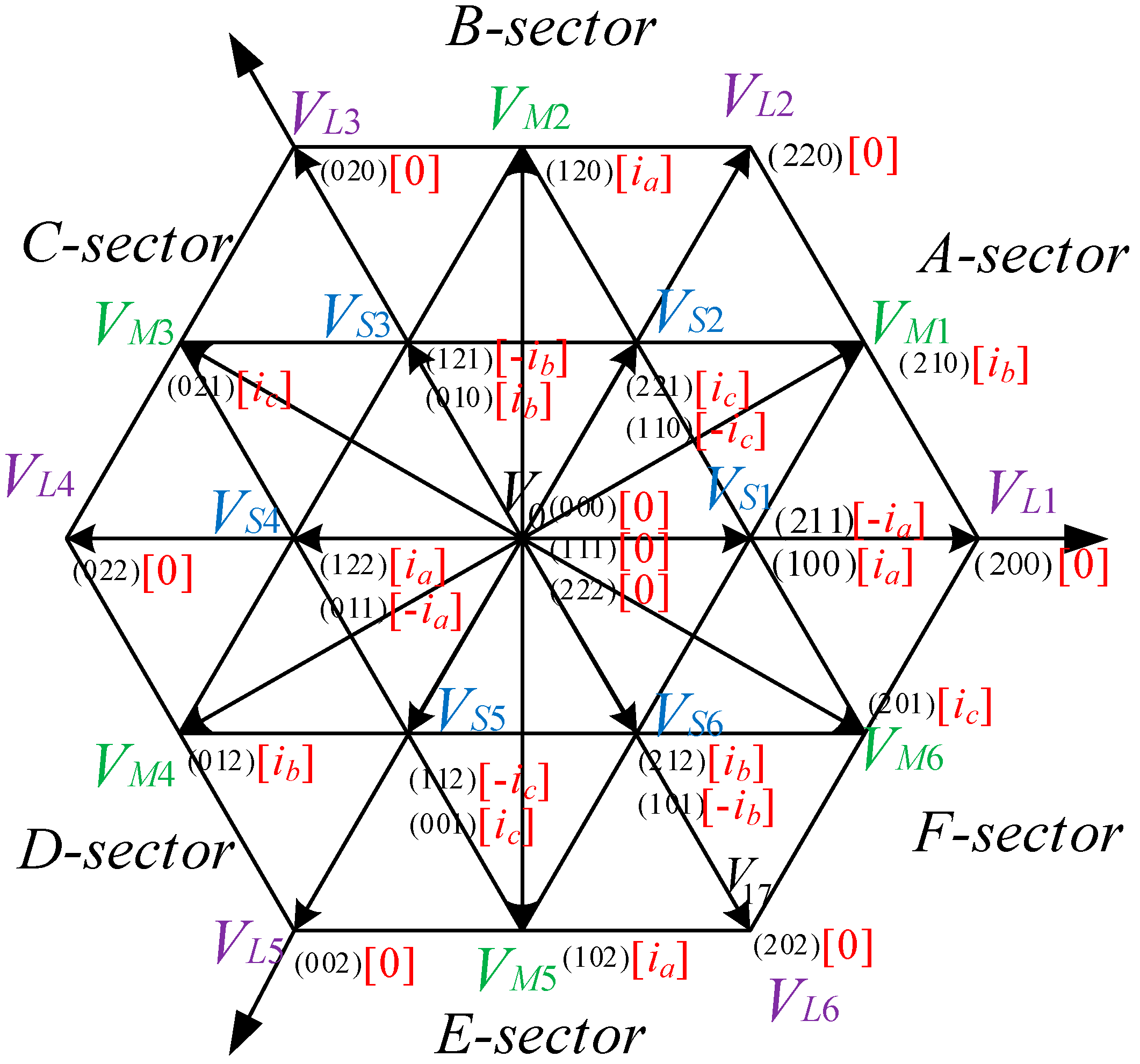
2. VSVPWM Modulation Principle of Diode Clamped Multi-Level Converter

Taking n = 3 as an example to introduce the implementation process of VSVPWM. Figure 1 shows a three-level space vector diagram with six sectors, the total output of the converter is 27 switching states with 19 voltage vectors, which are divided into zero vector (V0), small vector (VS1~VS6), medium vector (VM1~VM6) and large vector (VL1~VL6). The neutral current generated by each switch state of each voltage vector as shown in [], and it can be seen that the zero vector and the large vector do not affect the midpoint voltage of the DC side capacitor, while the two switches of the small vector have the opposite effect on it. Besides, the medium vector will also generate a neutral current. In order to realize the voltage balanced control of the midpoint of the DC-side capacitor during the stable state, the new virtual medium vector and virtual small vector are defined. Take the A-sector as an example, as shown in Figure 2, the sector is re-divided into five sub-sectors, i.e., A1~A5. The corresponding relationship between the virtual vectors in Figure 2 and vectors in Figure 1 is as follows:
(1) Virtual small vector. The virtual small vector is composed of a pair of redundant small vectors in the basic vector. The positive and negative small vectors each occupy half of the length and have the same action time. The virtual small vectors are constructed as follows:
{ V V S 1 = 1 / 2 × ( V S 1 ( 211 ) + V S 1 ( 100 ) ) V V S 2 = 1 / 2 × ( V S 2 ( 221 ) + V S 2 ( 110 ) )
(2) Virtual medium vector. The virtual medium vector is composed of one medium vector in the basic vector and two different small vectors adjacent to the medium vector. Each length is 1/3, and the action time is equal. In this way, as shown in Figure 1, the currents (ia + ic) generated by the switch state (100) and (221) of small vector and the current ib generated by the switch state (210) of medium vector cancel each other, the neutral current is zero, thereby achieving balanced control of the midpoint voltage of the capacitor. The construction equation of the virtual medium vector is:
V V M 1 = 1 / 3 × ( V S 1 ( 100 ) + V S 2 ( 221 ) + V M 1 ( 210 ) )
(3) Virtual large vector and virtual zero vector. The large and zero vectors in Figure 1 will not affect the midpoint current, so the virtual large and zero vectors can be directly replaced with the large and zero vectors in the basic vector.
Using the synthesized virtual medium vector instead of the medium vector in the original space vector diagram, the average neutral current of the multi-level topology converter in the unit switching cycle is zero when the connected load or grid is symmetrical, which will not cause the imbalance of the DC side capacitor voltage.
Similarly, for the four-level virtual space vector, as shown in Figure 3, the A sector is divided into 13 small sub-sectors, 11 new virtual vectors V1~V11 are defined. All these virtual vectors do not affect the midpoint voltage of the DC side capacitor, among which V5, V6, and V9 have two redundant states:
{ V 5 , 1 = 1 / 2 × ( V 311 + V 100 ) V 5 , 2 = 1 / 2 × ( V 322 + V 200 )
{ V 6 , 1 = 1 / 2 × ( V 331 + V 110 ) V 6 , 2 = 1 / 2 × ( V 332 + V 220 )
{ V 9 , 1 = 1 3 V 331 + 1 3 V 310 + 1 3 V 100 V 9 , 2 = 1 3 V 332 + 1 3 V 320 + 1 3 V 200
Define three variables x5, x6 and x9 as the redundant state allocation coefficients of the virtual space vectors V5, V6 and V9. The value range is [0, 1]. Then:
{ V 5 ( x 5 ) = x 5 V 5 , 1 + ( 1 x 5 ) V 5 , 2 V 6 ( x 6 ) = x 6 V 6 , 1 + ( 1 x 6 ) V 6 , 2 V 9 ( x 9 ) = x 9 V 9 , 1 + ( 1 x 9 ) V 9 , 2
The definition of a multi-level virtual space vector above four levels is the same as that of four levels, which defines more virtual space vectors and more redundant states, but all of them meet the basic requirement that the neutral current of the converter is zero. The division of the first sector of the virtual space vector graph of five-level and N-level is shown in Figure 4 and Figure 5.
In Figure 2, firstly, according to the command voltage vector to determine the number of the sub-sector, then using the adjacent three virtual vectors to compose the command voltage vector. Taking the three-level topology as an example, since the switch state of each virtual vector is determined, the modulation sequence and action time within the unit switch cycle are also determined, as shown in Table 1.
For the implementation of n-level VSVPWM, as the number of levels increases, the redundant switching states of some virtual voltage vectors also increases, so the switching sequence of the modulation output is not unique. If all switching states are used, i.e., the redundant state allocation coefficients xi of virtual space vectors Vi are not equal to 0 or 1, the sequence of the n-level converter modulated with VSVPWM method in any sub-sector is 2(3n−4) segments. Taking the A3 sub-sector as an example, the final output symmetric modulation sequence is: 100→200→210→211→…→m(m−2)(m−2)→m(m−1)(m−2)→m(m−1)(m−1)→…→n(n−2)(n−2)→n(n−1)(n−2)→n(n−1)(n−1)→nn(n−1)→n(n−1)(−1)→n(n−1)(n−2)→n(n−2)(n−2)→…→m(m−1)(m−1)→m(m−1)(m−2)→m(m−2)(m−2)→…→211→210→200→100.

3. The Essential Relationship between Diode Clamp Multi-Level Converter VSVPWM and MCBPWM

3.1. The Equivalent of Three-Level VSVPWM Modulation and MCBPWM Modulation

It can be seen from Table 1 that the modulation sequence of three-level VSVPWM in each sub-sector is 10 segments, but the traditional CBPWM can only output two levels per phase, and three-phase can output up to eight segments in the modulation sequence, so the traditional CBPWM modulation method cannot solve the above problem. This paper refers to the principle of modulation wave decomposition in reference [16] and decomposes n-level modulation waves into (n − 1) sub-modulation waves, so as to realize the output of multiple voltage states per phase. Assuming that the initial value of the modulated wave is Va*, and the number of levels is n = 5, four conventional CBPWM modulated waves Va1*, Va2*, Va3* and Va4* are obtained after decomposition, as shown in Figure 6. Then the same output as the modulated wave Va* can be achieved by the superposition of the output of the four conventional CBPWM modulation waves. Each sub-modulation wave intersects with the four in-phase stacked carriers respectively. After the superposition, the voltage of each phase contains five levels.
Taking the three-level VSVPWM sub-sector A3 as an example, in one switching cycle, phase A and phase C output two levels respectively, and phase B output three-level states of 0, 1, and 2, so it is necessary to decompose the B-phase modulation wave. Set the initial value of the B-phase modulation wave is Vb, and the values after decomposition are V b 1 * and V b 2 * . In Figure 7, the effect of the three-level output of the B-phase modulation wave within one switching cycle can be achieved by the superposition of conventional CBPWM sub-modulation waves V b 1 * and V b 1 * , through the modulation wave decomposition strategy, the output of multiple levels per switching period is realized.
VSVPWM is equivalent to injecting the zero-sequence component into the Multi-modulation carrier CBPWM (MCBPWM) to obtain the same output waveform as VSVPWM. By obtaining the zero-sequence component, the equivalent relationship of the switching sequence between the VSVPWM and the MCBPWM can be obtained. At this time, the sub-modulation waves obtained by the decomposition of the B-phase initial modulation waves can directly control the on-off state of the B-phase switch tubes. It can be seen from Table 1 that the VSVPWM modulation output in sector A3 is a 10-segment symmetric modulation sequence: 100→200→210→211→221→221→211→210→200→100. The action time of each switch state of the virtual space vector is shown in Figure 7, where, V a * , V b * and V c * are three-phase MCBPWM modulation waves, V t 1 * and V t 2 * are triangular carrier waves. Next, the relationship between MCBPWM and VSVPWM is derived through strict theoretical calculation.
In Figure 2, the vectors in the A3 area can be synthesized by the adjacent virtual vectors VVSl, VVMl and VVLl, the virtual vector action times are TVSl, TVMl, and TVLl, respectively, which satisfy TS = TVSl + TVMl + TVLl. According to Equations (1) and (2), the small vector VSl (100) constitutes the virtual vector VVSl and VVMl, then the action time of the small vector VSl (100) in a switching cycle is: TS1 = TVS1/2 + TVM1/3. Considering the symmetry of the space vector modulation sequence in a switching cycle, the action time of the small vector VSl (100) in the first half of the switching cycle in Figure 7 is: TS1 = TVS1/4 + TVM1/6, the action time analysis of other vectors is similar.
In Figure 7, in a switching cycle, according to the volt-second balance principle:
{ ( 1 2 T V S 1 + 1 3 T V M 1 + 2 T V L 1 + 1 3 T V M 1 + 1 2 T V S 1 ) V d c 2 = T s V a b ( 1 3 T V M 1 + 1 3 T V M 1 ) V d c 2 = T s V b c
Considering T V S 1 + T V M 1 + T V L 1 = T S :
{ T V L 1 = ( V b c / 2 + V a b V d c / 2 1 ) T S T V M 1 = 3 2 V b c V d c / 2 T S T V S 1 = ( 2 2 V b c + V a b V d c / 2 ) T S
According to the relevant characteristic of similar triangles, there are:
{ V d c 2 V a 1 * V d c 2 = 1 3 T V M 1 + 1 2 T V S 1 T S V a 2 * = 0 V b 1 * V d c 2 = 1 3 T V M 1 T S 0 V b 2 * V d c 2 = 1 3 T V M 1 + 1 2 T V S 1 + T V L 1 T S V c 1 * = 0 V c 2 * + V d c 2 V d c 2 = 1 3 T V M 1 + 1 2 T V S 1 T S
The value of the two sub-modulated waves in each phase of the three phases is as follows:
{ V a 1 * = 1 2 × V a 1 2 × V c V a 2 * = 0 V b 1 * = 1 2 × V b 1 2 × V c V b 2 * = 1 2 × V a + 1 2 × V b V c 1 * = 0 V c 2 * = 1 2 × V c 1 2 × V a
Substituting Equation (10) into equation V x * = V x 1 * + V x 2 * ( x = a , b , c ) :
{ V a * = V a + V z V b * = V b + V z V c * = V c + V z V z = 1 2 × V a 1 2 × V c
Based on the equivalent relationship of the three-level VSVPWM and MCBPWM, three-phase multiple sub-modulation waves of Equation (10) with the CBPWM method can achieve the same output effect as VSVPWM. By comparing each sub-modulated wave and the corresponding triangular carrier directly to determine the on-off status of each switch tube, MCBPWM modulation strategy simplifies the modulation process and reduces the amount of calculation.
In the other sub-sectors of A-sector, the same zero-sequence component as in Equation (11) is obtained. Let Vmax, Vmid, and Vmin represent the maximum, middle, and minimum of the modulation waves in the original phase A, B, and C respectively. Through the same derivation method, in other large sectors (B~F) of the diode clamped multi-level hexagonal space vector diagram, injecting the zero-sequence component obtained by the decomposition of the modulation wave into the three-phase modulation wave, the equivalent relationship of the three-level 10-segment VSVPWM and MCBPWM can be achieved. The expression of the zero-sequence component can be simplified as follows:
V z = 1 2 ( V max + V min ) .
The expressions sub-modulation waves of each phase are as follows:
{ V max 1 * = 1 2 × V max 1 2 × V min V max 2 * = 0 V m i d 1 * = 1 2 × V m i d 1 2 × V min V m i d 2 * = 1 2 × V max + 1 2 × V m i d V min 1 * = 0 V min 2 * = 1 2 × V min 1 2 × V max

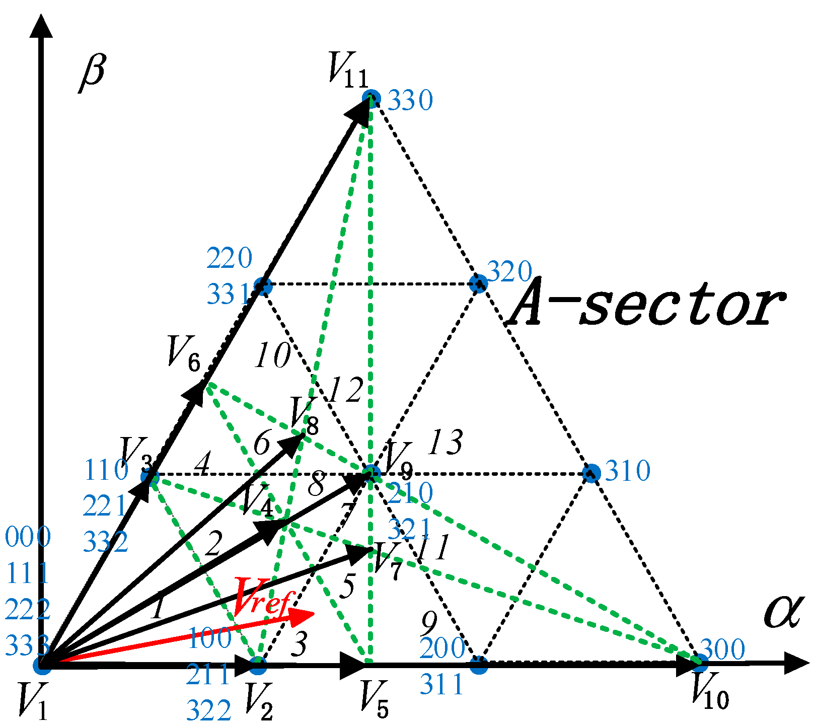
3.2. The Equivalent of Four-Level VSVPWM Modulation and MCBPWM Modulation

When n = 4, the four-level virtual space vector diagram is divided into 13 small sectors in the first sector. Unlike the three-level, there is more than one synthesis method for the newly synthesized four-level virtual space vector. As mentioned above, take the A3 sub-sector in the first sector of the four-level virtual space vector diagram as an example, the required reference vector Vref is synthesized by V2, V4 and V5, and V5 contains a redundant state whose allocation factor is represented by x5, so the output 16-segment modulation sequence is: 100→200→210→211→311→321→322→332→ 332→322→321→311→211→210→200→100, as shown in Figure 8.
Similar to the analysis in Section A, the expressions of three-phase four sub-modulated waves can be obtained as follows:
{ V a 1 * = 1 3 V a c + 1 6 V d c V a 2 * = 2 3 V a c 1 3 ( x 5 + 1 ) V b c x 5 V a b + 2 x 5 1 6 V d c V a 3 * = 1 6 V d c { V b 1 * = 1 3 V b c + 1 6 V d c V b 2 * = 2 3 V a c + ( 1 x 5 ) V a b + 1 3 ( 3 x 5 ) V b c + 2 x 5 1 6 V d c V b 3 * = 1 3 V a b 1 6 V d c { V c 1 * = 1 6 V d c V c 2 * = 2 3 V a c + ( 1 x 5 ) V a b + 2 x 5 3 V b c + 2 x 5 1 6 V d c V c 3 * = 1 3 V a c 1 6 V d c
According to V x * = V x 1 * + V x 2 * + V x 3 * ( x = a , b , c ) , Equation (14) can be solved as:
{ V a * = V a + V z V b * = V b + V z V c * = V c + V z V z = x 5 V a + ( 2 3 x 5 1 3 ) V b + x 5 2 3 V c + 2 x 5 1 6 V d c
It can be seen that the expression of the zero-sequence component and the duty cycle of the redundant state are related, but when the redundant switching state is used on average, that is, x5 = 1/2, the expression of the zero-sequence component can be simplified as:
V z = 1 2 ( V a + V c ) .
According to the same derivation, when the other sectors respectively set x5 = x6 = x9 = 1/2, the same expression of the zero-sequence component can be obtained:
V z = 1 2 ( V max + V min ) .
Correspondingly, the value of each phase sub-modulation wave modulated by MCBPWM is:
{ V max 1 * = 1 3 V max 1 3 V min + 1 6 V d c V max 2 * = 1 6 V max 1 6 V min V max 3 * = 1 6 V d c { V m i d 1 * = 1 3 V m i d 1 3 V min + 1 6 V d c V m i d 2 * = 1 6 V max + 1 3 V m i d 1 6 V min V m i d 3 * = 1 3 V max + 1 3 V m i d 1 6 V d c { V min 1 * = 1 6 V d c V min 2 * = 1 6 V max + 1 6 V min V min 3 * = 1 3 V max + 1 3 V min 1 6 V d c

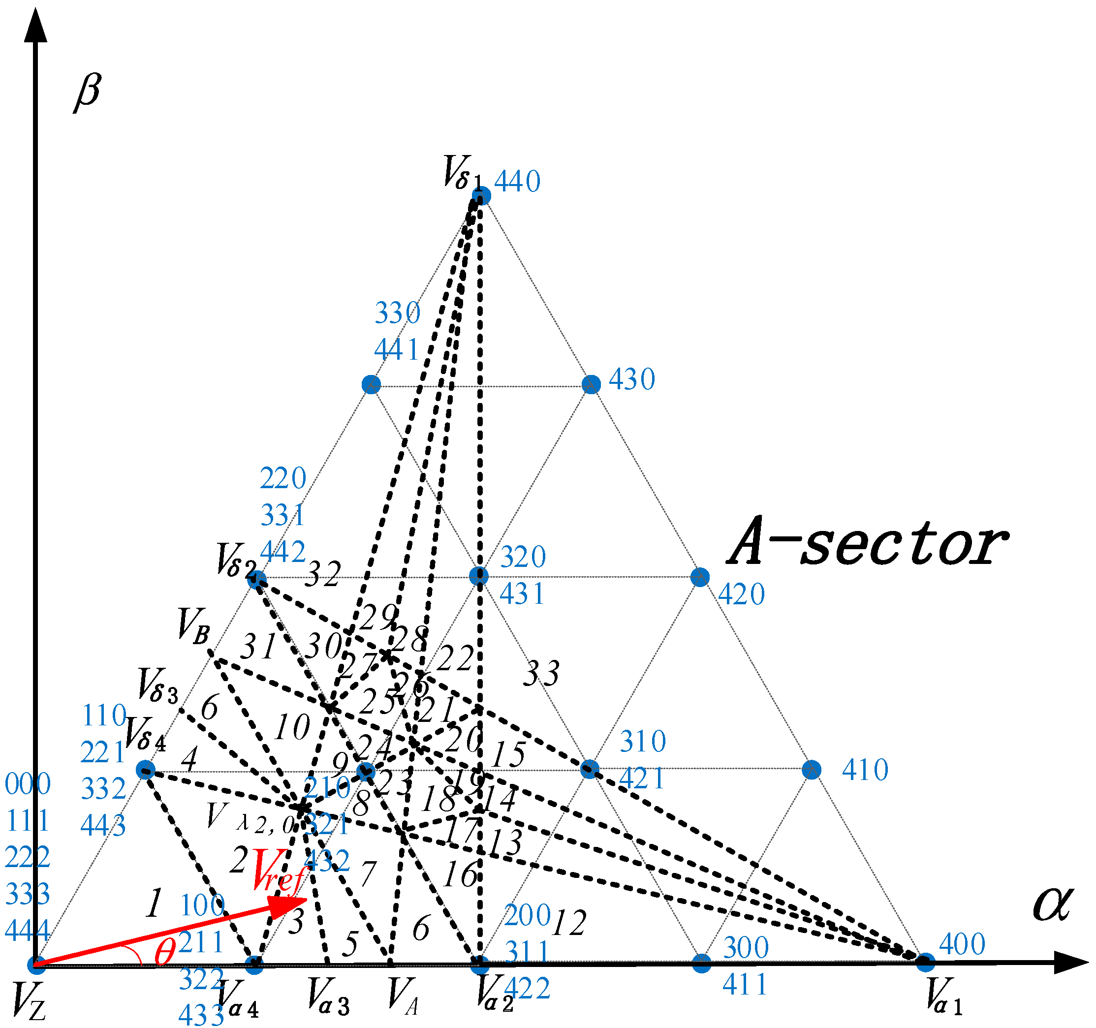
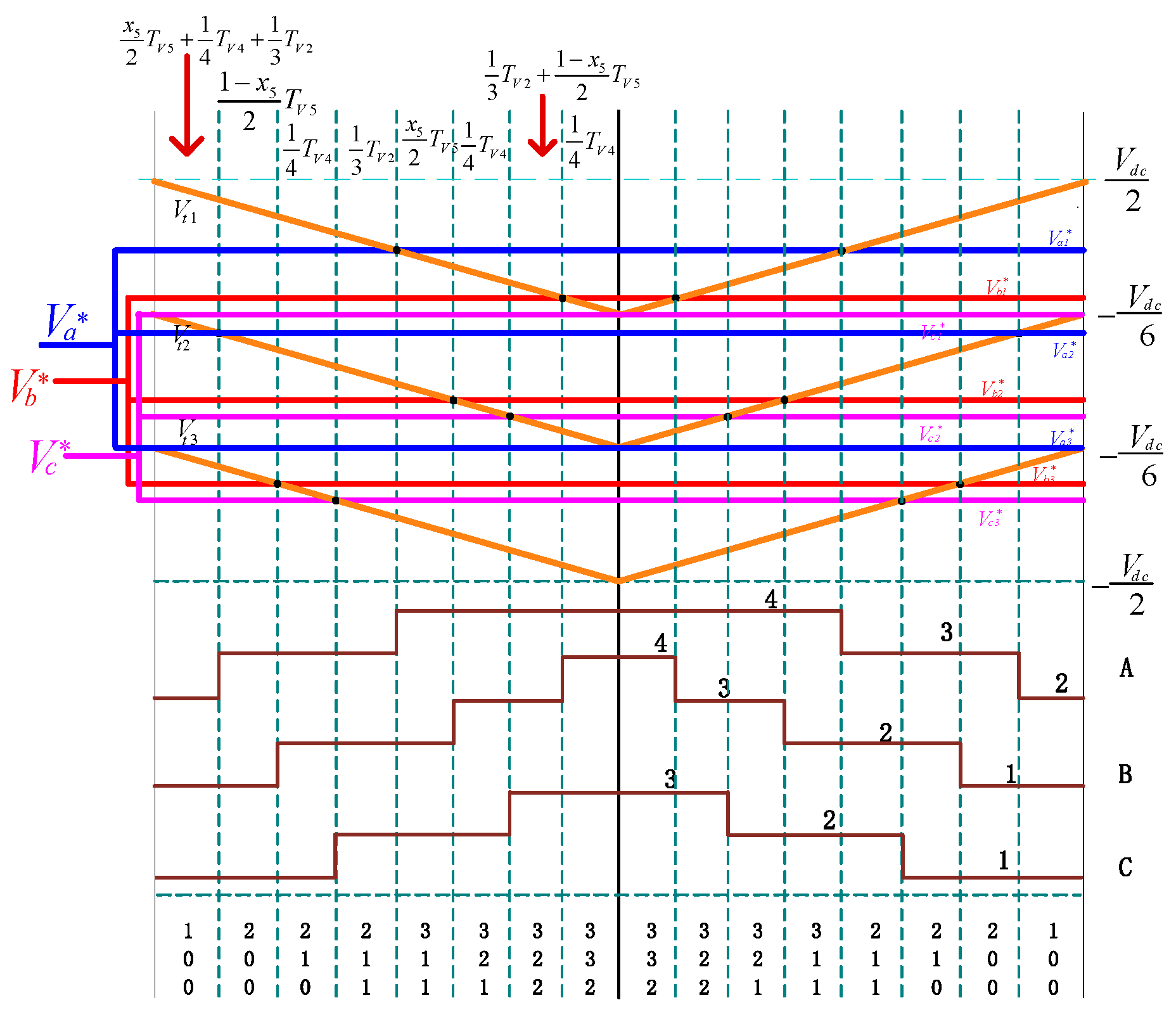
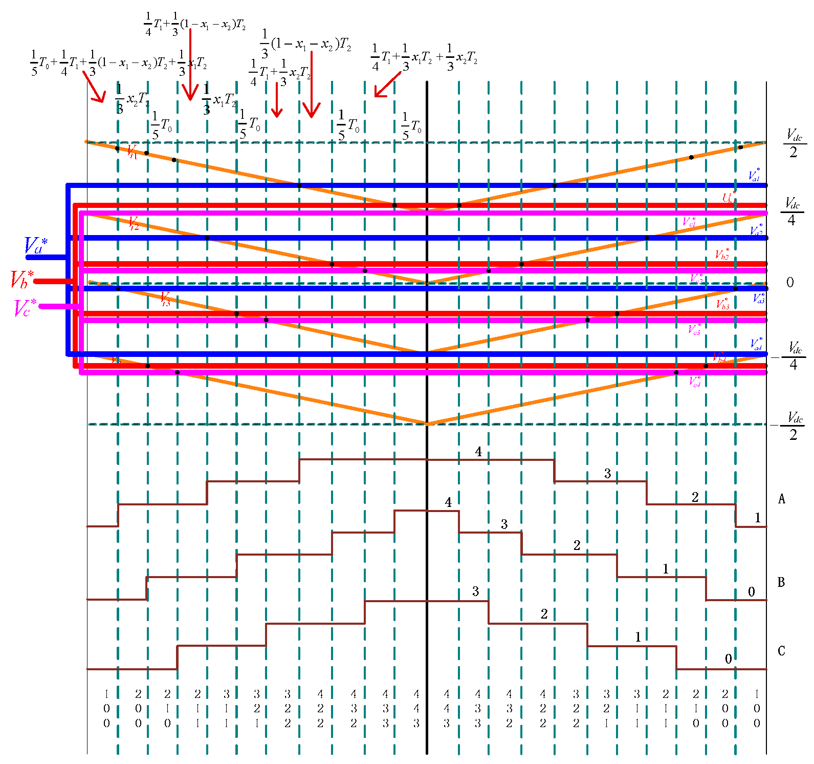
3.3. Equivalence of N-Level VSVPWM Modulation and MCBPWM Modulation

Similarly, taking the five-level A3 sector as an example, as shown in Figure 9, the virtual vectors Vα3, Vα4 and Vλ2,0 are used to synthesize the reference vector, and the corresponding action times are T2, T1 and T0 respectively. Vα3 has three redundant states, the duty cycles of the redundant states are represented by x1, x2 and (1-x1-x2). Same as four levels, the modulation wave is divided into four sub-modulation waves, and the same 22 segment symmetrical switching sequence as VSVPWM modulation can be obtained: 100→200→210→211→311→321→322→422→432→433→443→443→433→432→422→322→321→311→211→210→200→100. As shown in Figure 9, the expression of zero-sequence component is:
V z = ( x 1 + 2 x 2 3 2 ) V a + 3 4 ( 1 x 1 2 x 2 ) V b 1 4 ( 1 + x 1 + 2 x 2 ) V c + 1 x 1 2 x 2 4 V d c
Based on this equivalence relation, the values of each phase of each sub-modulation wave of MCBPWM modulation strategy are obtained as follows:
{ V a 1 * = 1 4 V a c + 1 4 V d c V a 2 * = 1 4 ( x 1 + x 2 ) V b c 1 4 ( 2 4 x 1 4 x 2 ) V a b + 1 x 1 x 2 4 V d c V a 3 * = 1 4 ( 4 x 2 1 ) V a b + 1 4 x 2 V b c x 2 4 V d c V a 4 * = V d c 4 { V b 1 * = 1 4 V b c + 1 4 V d c V b 2 * = 1 4 ( 4 x 1 + 4 x 2 3 ) V a b + 1 4 ( x 1 + x 2 ) V b c + 1 x 1 x 2 4 V d c V b 3 * = 1 4 ( 4 x 2 2 ) V a b + 1 4 x 2 V b c x 2 4 V d c V b 4 * = 1 4 V a b 1 4 V d c { V c 1 * = V d c 4 V c 2 * = 1 4 ( 4 x 1 + 4 x 2 3 ) V a b + 1 4 ( x 1 + x 2 1 ) V b c + 1 x 1 x 2 4 V d c V c 3 * = 1 4 ( 4 x 2 2 ) V a b + 1 4 ( x 2 1 ) V b c x 2 4 V d c V c 4 * = 1 4 V a c 1 4 V d c
According to Equation (19), the expression of the zero-sequence component and the duty cycle of the redundant state are related, but when the redundant switching state is used on average, i.e., x1 = x2 = 1/3. The expression of the zero-sequence can be simplified as:
V z = 1 2 ( V a + V c ) .
According to the same derivation, when xi = 1/3 in other sectors, the same expression of zero sequence component can be obtained:
V z = 1 2 ( V max + V min ) .
The corresponding values of each phase sub-modulated wave are:
{ V max 1 * = 1 4 V max 1 4 V min + 1 4 V d c V max 2 * = 1 6 V max 1 6 V min + 1 12 V d c V max 3 * = 1 12 V max 1 12 V min 1 12 V d c V max 4 * = V d c 4 { V m i d 1 * = 1 4 V m i d 1 4 V min + 1 4 V d c V m i d 2 * = 1 12 V max + 1 4 V m i d 1 6 V min + 1 12 V d c V m i d 3 * = 1 6 V max + 1 4 V m i d 1 12 V min 1 12 V d c V m i d 4 * = 1 4 V max + 1 4 V m i d 1 4 V d c { V min 1 * = V d c 4 V min 2 * = 1 12 V max + 1 12 V min + 1 12 V d c V min 3 * = 1 6 V max + 1 6 V min 1 12 V d c V min 4 * = 1 4 V max + 1 4 V min 1 4 V d c
For the n-level main circuit, each phase can output n levels. In the first sector of the virtual space vector diagram in Figure 5, there are (n2 − 2n + 3) virtual vectors in total, some virtual vectors contain (n − 2) switch states. If the switch states of these redundant vectors are used on average, the modulation sequence of the 2 × (3n − 4) segment will be formed. Finally, the zero-sequence component superimposed of each phase is obtained as follows:
V z = 1 2 ( V max + V min ) n = 3 , 4 , 5.... n .
When n = 3, 5, 7, …, or n = 4, 6, 8, …, the equation expressions of (n − 1) sub-modulation waves as shown in the Appendix A section.
In this way, the two can be connected by the zero-sequence component to achieve the equivalent of any level VSVPWM sequence and the MCBPWM sequence. Based on this equivalent relationship, the MCBPWM method is proposed to realize the same output as VSVPWM by multiple sub-modulated waves obtained by the decomposition of modulated waves. In the virtual space vector of any level, by adopting the MCBPWM modulation strategy, the control of the midpoint voltage of the DC side capacitor can be achieved, and the modulation effect of the virtual space vector is realized by the simple and easy MCBPWM method, which greatly simplifies the modulation process and reduces the calculation amount and CPU occupation rate.

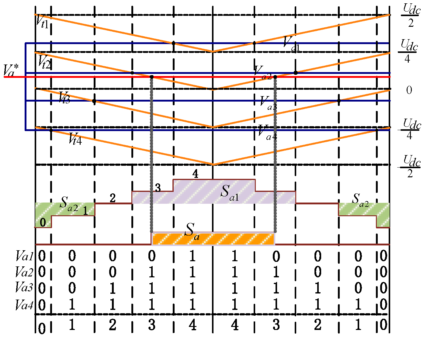
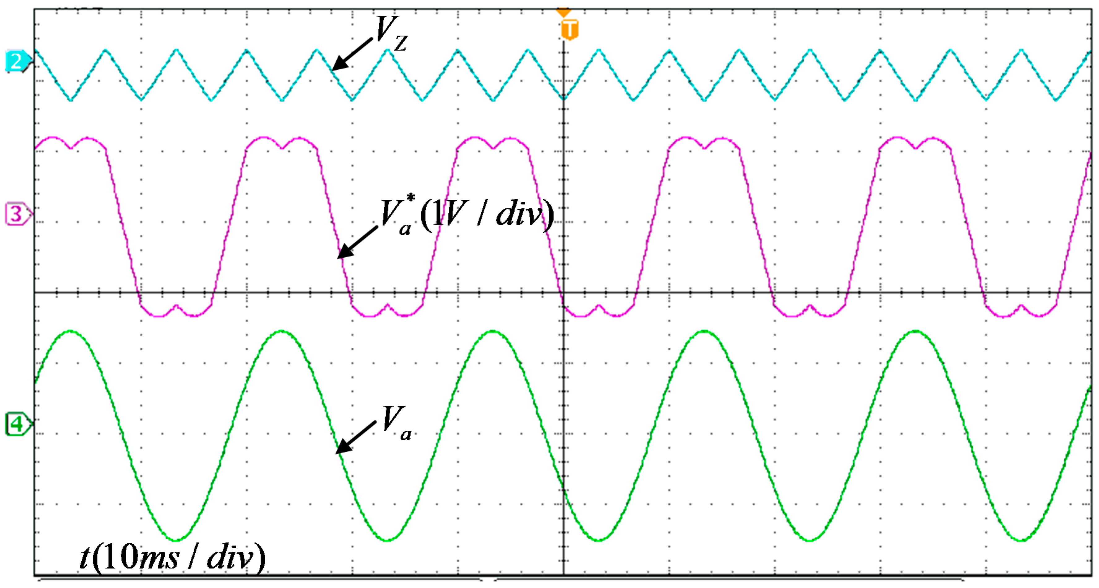
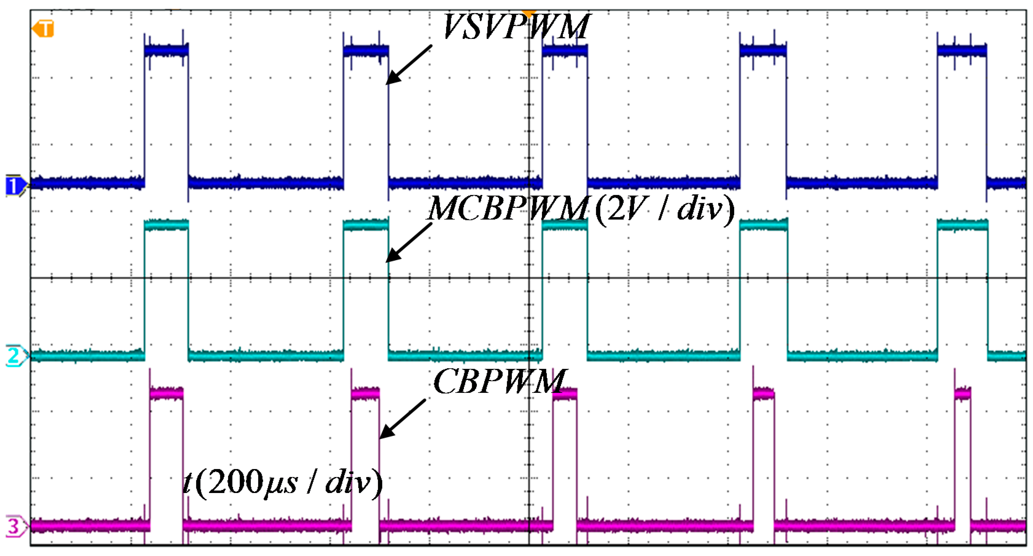
4. Experiment and Result Analysis

In order to verify the correctness of the equivalent relationship between two, the VSVPWM and MCBPWM modulation sequence output of the open-loop inverter under a certain modulation ratio is realized on the experimental platform of digital signal processing + field-programmable gate array (DSP + FPGA). Among them, DSP selects TMS320F28335 of the TI company, which mainly realizes control and calculation of the entire system, the output of DSP is sent to FPGA. FPGA chooses EP2C35F484C8 of Altera Company’s Cyclone II series, which mainly generates pulse-width modulation (PWM) signals. The FPGA does not send gate signals to drive any power electronic switches but sends the switching states generated by the modulation algorithms to the oscilloscope for observation [20,21]. The other parts are used for power supply, communication and protection. The experimental system is shown in Figure 10.
When the number of levels is n = 3 and the modulation ratio is 0.3. Given VSVPWM modulation sequence, the zero-sequence component injected into the MCBPWM sine wave can be obtained through the equivalent relationship.
Figure 11 shows A-phase sub-modulation waves Va1* and Va2* modulated by MCBPWM that output the same 10-segment modulation sequence as VSVPWM. Va* is the sum of two sub-modulation waves of phase A.
In Figure 12, VZ represents the zero-sequence component required to achieve the equivalent of MCBPWM and VSVPWM. It can be seen that the zero-sequence component VZ is superimposed on the A-phase sinusoidal modulation wave, and the same modulation wave Va* as the double modulation wave MCBPWM can be obtained. This proves the correctness of the modulation wave decomposition.
Figure 13 shows the switching states of the two switching tubes Sa1 and Sa2 above the A-bridge arm of three-level diode clamp converter, and the output switching state of phase A is Sa. When the VSVPWM method is used to output the 10-segment switching sequence, some switching cycles can output the three-level switching state.
Figure 14 shows the switching state of A-phase Sa1 under three modulation modes of VSVPWM, MCBPWM and CBPWM. The switching state of VSVPWM and MCBPWM are exactly the same, indicating that the MCBPWM can realize the same modulation effect as VSVPWM. It can be seen from the above experimental waveform that the total output results and the results of each switch state under the two modulation methods are exactly the same, which proves the correctness of the equivalence relationship between VSVPWM and MCBPWM.

5. Discussion

This paper mainly conducted an in-depth study on the equivalent relationship between the VSVPWM and MCBPWM. By decomposing each phase modulation wave, through strict theoretical derivation and mathematical calculation, the zero-sequence component to be injected in the three-phase sinusoidal modulation wave is obtained, and the in-phase stacked CBPWM is performed using each decomposed sub-modulation wave. It has the same control effect as VSVPWM, successfully achieves the equivalent of VSVPWM and MCBPWM with any level and any number of segments, simplifies the analysis of VSVPWM, solves the voltage imbalance problem on the DC side of three-phase NPC, and perfects the weakness of three-phase NPC multi-level converter. In this paper, the equivalent relationship between VSVPWM and MCBPWM is deduced to the n-th level, which solves the difficulty of VSVPWM caused by the increase in the number of levels. It has important significance for the application of multi-level NPC converters.

Author Contributions

Conceptualization, Y.H. and J.L.; methodology, C.L., Y.L.; software, C.L.; validation, Y.H., J.L., C.L. and Y.L.; formal analysis, C.L.; investigation, C.L.; resources, Y.L.; data curation, Y.L.; writing—original draft preparation, C.L.; writing—review and editing, C.L.; visualization, C.L.; supervision, Y.H.; project administration, Y.H.; funding acquisition, Y.H. All authors have read and agreed to the published version of the manuscript.

Funding

This project is supported by projects of the China Southern Power Grid Corporation (GDKJXM20172770), the National Natural Science Foundation of China (51777158), the Natural science Basic Research Plan in Shanxi Province of China (2018JM5008), Science and Technology Research Plan in Xian City of China (201805034YD12CG18-2).

Conflicts of Interest

The authors declare no conflict of interest.

Abbreviations

The following abbreviations are used in this manuscript:
AbbreviationFull Name
THDTotal harmonic distortion
PWMPulse-width modulation
VSVPWMVirtual space vector pulse-width modulation
CBPWMCarrier-based pulse-width modulation
SVPWMSpace vector pulse-width modulation
MCBPWMMulti-modulation carrier CBPWM
NPCNeutral-point-clamped
DSPDigital signal processing
FPGAField programmable gate array

Appendix A

When n = 3, 5, 7, …, the values of (n − 1) sub-modulation waves are:
{ V max 1 * = 1 n 1 V max 1 n 1 V min + [ 1 2 1 n 1 ] V d c                                                                                                                                         V max i * = n i 1 ( n 1 ) ( n 2 ) V max n i 1 ( n 1 ) ( n 2 ) V min + [ 1 2 i 1 n 1 n i 1 ( n 1 ) ( n 2 ) ] V d c                                                                                                                                         V max ( n 1 2 ) * = 1 2 ( n 2 ) V max 1 2 ( n 2 ) V min + n 3 2 ( n 1 ) ( n 2 ) V d c V max ( n + 1 2 ) * = n 3 2 ( n 1 ) ( n 2 ) V max n 3 2 ( n 1 ) ( n 2 ) V min n 3 2 ( n 1 ) ( n 2 ) V d c                                                                                                                                         V max ( n i ) * = i 1 ( n 1 ) ( n 2 ) V max i 1 ( n 1 ) ( n 2 ) V min [ 1 2 i 1 n 1 n i 1 ( n 1 ) ( n 2 ) ] V d c                                                                                                                                         V max ( n 1 ) * = ( 1 2 1 n 1 ) V d c { V m i d 1 * = 1 n 1 V m i d 1 n 1 V min + [ 1 2 1 n 1 ] V d c                                                                                                                                         V m i d i * = i 1 ( n 1 ) ( n 2 ) V max + 1 n 1 V m i d n i 1 ( n 1 ) ( n 2 ) V min + [ 1 2 i 1 n 1 n i 1 ( n 1 ) ( n 2 ) ] V d c                                                                                                                                         V m i d ( n 1 2 ) * = n 3 2 ( n 1 ) ( n 2 ) V max + 1 n 1 V m i d 1 2 ( n 2 ) V min + n 3 2 ( n 1 ) ( n 2 ) V d c V m i d ( n + 1 2 ) * = 1 2 ( n 2 ) V max + 1 n 1 V m i d n 3 2 ( n 1 ) ( n 2 ) V min n 3 2 ( n 1 ) ( n 2 ) V d c                                                                                                                                         V m i d ( n i ) * = n i 1 ( n 1 ) ( n 2 ) V max + 1 n 1 V m i d i 1 ( n 1 ) ( n 2 ) V min [ 1 2 i 1 n 1 n i 1 ( n 1 ) ( n 2 ) ] V d c                                                                                                                                         V m i d ( n 1 ) * = 1 n 1 V max + 1 n 1 V m i d ( 1 2 1 n 1 ) V d c { V min 1 * = ( 1 2 1 n 1 ) V d c                                                                                                                                         V min i * = i 1 ( n 1 ) ( n 2 ) V max + i 1 ( n 1 ) ( n 2 ) V min + [ 1 2 i 1 n 1 n i 1 ( n 1 ) ( n 2 ) ] V d c                                                                                                                                         V min ( n 1 2 ) * = n 3 2 ( n 1 ) ( n 2 ) V max + n 3 2 ( n 1 ) ( n 2 ) V min + n 3 2 ( n 1 ) ( n 2 ) V d c V min ( n + 1 2 ) * = 1 2 ( n 2 ) V max + 1 2 ( n 2 ) V min n 3 2 ( n 1 ) ( n 2 ) V d c                                                                                                                                         V min ( n i ) * = n i 1 ( n 1 ) ( n 2 ) V max + n i 1 ( n 1 ) ( n 2 ) V min [ 1 2 i 1 n 1 n i 1 ( n 1 ) ( n 2 ) ] V d c                                                                                                                                         V min ( n 1 ) * = 1 n 1 V max + 1 n 1 V min [ 1 2 1 n 1 ] V d c
When n = 4, 6, 8, …, the values of (n − 1) sub-modulated wave are:
{ V max 1 * = 1 n 1 V max 1 n 1 V min + [ 1 2 1 n 1 ] V d c                                                                                                                       V max i * = n i 1 ( n 1 ) ( n 2 ) V max n i 1 ( n 1 ) ( n 2 ) V min + [ 1 2 i 1 n 1 n i 1 ( n 1 ) ( n 2 ) ] V d c                                                                                                                       V max ( n 2 ) * = n 2 2 ( n 1 ) ( n 2 ) V max n 2 2 ( n 1 ) ( n 2 ) V min                                                                                                                       V max ( n i ) * = i 1 ( n 1 ) ( n 2 ) V max i 1 ( n 1 ) ( n 2 ) V min [ 1 2 i 1 n 1 n i 1 ( n 1 ) ( n 2 ) ] V d c                                                                                                                       V max ( n 1 ) * = ( 1 2 1 n 1 ) V d c { V m i d 1 * = 1 n 1 V m i d 1 n 1 V min + [ 1 2 1 n 1 ] V d c                                                                                                                       V m i d i * = i 1 ( n 1 ) ( n 2 ) V max + 1 n 1 V m i d n i 1 ( n 1 ) ( n 2 ) V min + [ 1 2 i 1 n 1 n i 1 ( n 1 ) ( n 2 ) ] V d c                                                                                                                         V m i d ( n 2 ) * = n 2 2 ( n 1 ) ( n 2 ) V max + 1 n 1 V m i d 1 2 ( n 2 ) V min + n 2 2 ( n 1 ) ( n 2 ) V d c                                                                                                                       V m i d ( n i ) * = n i 1 ( n 1 ) ( n 2 ) V max + 1 n 1 V m i d i 1 ( n 1 ) ( n 2 ) V min [ 1 2 i 1 n 1 n i 1 ( n 1 ) ( n 2 ) ] V d c                                                                                                                       V m i d ( n 1 ) * = 1 n 1 V max + 1 n 1 V m i d ( 1 2 1 n 1 ) V d c { V min 1 * = ( 1 2 1 n 1 ) V d c                                                                                                                       V min i * = i 1 ( n 1 ) ( n 2 ) V max + i 1 ( n 1 ) ( n 2 ) V min + [ 1 2 i 1 n 1 n i 1 ( n 1 ) ( n 2 ) ] V d c                                                                                                                       V min ( n 2 ) * = n 2 2 ( n 1 ) ( n 2 ) V max + n 2 2 ( n 1 ) ( n 2 ) V min                                                                                                                   V min ( n i ) * = n i 1 ( n 1 ) ( n 2 ) V max + n i 1 ( n 1 ) ( n 2 ) V min [ 1 2 i 1 n 1 n i 1 ( n 1 ) ( n 2 ) ] V d c                                                                                                                       V min ( n 1 ) * = 1 n 1 V max + 1 n 1 V min [ 1 2 1 n 1 ] V d c

References

  1. Jiang, W.; Wang, P.; Ma, M.; Wang, J.; Li, J.; Li, L.; Chen, K.; Weidong, J. A Novel Virtual Space Vector Modulation With Reduced Common-Mode Voltage and Eliminated Neutral Point Voltage Oscillation for Neutral Point Clamped Three-Level Inverter. IEEE Trans. Ind. Electron. 2019, 67, 884–894. [Google Scholar] [CrossRef]
  2. Wu, X.; Tan, G.; Ye, Z.; Yao, G.; Liu, Z.; Liu, G. Virtual-Space-Vector PWM for a Three-Level Neutral-Point-Clamped Inverter With Unbalanced DC-Links. IEEE Trans. Power Electron. 2018, 33, 2630–2642. [Google Scholar] [CrossRef]
  3. Alhosaini, W.; Wu, Y.; Zhao, Y. An Enhanced Model Predictive Control Using Virtual Space Vectors for Grid-Connected Three-Level Neutral-Point Clamped Inverters. IEEE Trans. Energy Convers. 2019, 34, 1963–1972. [Google Scholar] [CrossRef]
  4. Liu, G.; Wang, D.; Wang, M.; Zhu, C.; Wang, M. Neutral-Point Voltage Balancing in Three-Level Inverters Using an Optimized Virtual Space Vector PWM with Reduced Commutations. IEEE Trans. Ind. Electron. 2018, 65, 6959–6969. [Google Scholar] [CrossRef]
  5. Xiang, C.-Q.; Shu, C.; Han, D.; Mao, B.-K.; Wu, X.; Yu, T.-J.; Chao-Qun, X.; Cheng, S.; Ding, H.; Bing-Kui, M.; et al. Improved Virtual Space Vector Modulation for Three-Level Neutral-Point-Clamped Converter With Feedback of Neutral-Point Voltage. IEEE Trans. Power Electron. 2018, 33, 5452–5464. [Google Scholar] [CrossRef]
  6. Tan, L.; Wu, B.; Narimani, M.; Xu, D.; Liu, J.; Cheng, Z.; Zargari, N.R. A Space Virtual-Vector Modulation With Voltage Balance Control for Nested Neutral-Point Clamped Converter Under Low Output Frequency Conditions. IEEE Trans. Power Electron. 2017, 32, 3458–3466. [Google Scholar] [CrossRef]
  7. Hu, C.; Yu, X.; Holmes, D.G.; Shen, W.; Wang, Q.; Luo, F.; Liu, N. An Improved Virtual Space Vector Modulation Scheme for Three-Level Active Neutral-Point-Clamped Inverter. IEEE Trans. Power Electron. 2016, 32, 7419–7434. [Google Scholar] [CrossRef]
  8. Tian, K.; Wang, J.; Wu, B.; Cheng, Z.; Zargari, N.R. A Virtual Space Vector Modulation Technique for the Reduction of Common-Mode Voltages in Both Magnitude and Third-Order Component. IEEE Trans. Power Electron. 2015, 31, 839–848. [Google Scholar] [CrossRef]
  9. Song, W.; Wang, S.; Ge, X.; Xiong, C.; Feng, X. Single-phase three-level space vector pulse width modulation algorithm for grid-side railway traction converter and its relationship of carrier-based pulse width modulation. IET Electr. Syst. Transp. 2014, 4, 78–87. [Google Scholar] [CrossRef]
  10. Busquets-Monge, S.; Somavilla, S.; Bordonau, J.; Boroyevich, D. A novel modulation for the comprehensive neutral-point balancing in the three-level NPC inverter with minimum output switching-frequency ripple. In Proceedings of the 2004 IEEE 35th Annual Power Electronics Specialists Conference (IEEE Cat. No.04CH37551), Aachen, Germany, 20–25 June 2004; Institute of Electrical and Electronics Engineers (IEEE): Piscataway, NJ, USA, 2004; Volume 1–6, pp. 4226–4232. [Google Scholar]
  11. Busquets-Monge, S.; Bordonau, J.; Rocabert, J. A Virtual-Vector Pulsewidth Modulation for theFour-Level Diode-Clamped DC–AC Converter. IEEE Trans. Power Electron. 2008, 23, 1964–1972. [Google Scholar] [CrossRef]
  12. Busquets-Monge, S.; Alepuz, S.; Rocabert, J.; Bordonau, J. Pulsewidth Modulations for the Comprehensive Capacitor Voltage Balance of n-Level Three-Leg Diode-Clamped Converters. IEEE Trans. Power Electron. 2009, 24, 1364–1375. [Google Scholar] [CrossRef] [Green Version]
  13. Fang, H.; Ge, X.; Song, W.; Ding, R.; Feng, X. Relationship between two-level space-vector pulse-width modulation and carrier-based pulse-width modulation in the over-modulation region. IET Power Electron. 2014, 7, 189–199. [Google Scholar] [CrossRef]
  14. Yao, W.X.; Hu, H.B.; Lu, Z.Y. Comparisons of space-vector modulation and carrier-based modulation of multi-level inverter. IEEE Trans. Power Electron. 2008, 23, 45–51. [Google Scholar]
  15. Song, W.; Feng, X.; Smedley, K.M. A Carrier-Based PWM Strategy With the Offset Voltage Injection for Single-Phase Three-Level Neutral-Point-Clamped Converters. IEEE Trans. Power Electron. 2012, 28, 1083–1095. [Google Scholar] [CrossRef]
  16. Chen, J.; He, Y.; Hasan, S.U.; Liu, J.J. A Comprehensive Study on Equivalent Modulation Waveforms of the SVM Sequence for Three-Level Inverters. IEEE Trans. Power Electron. 2015, 30, 7149–7158. [Google Scholar] [CrossRef]
  17. He, Y.; Liu, Y.; Lei, C.; Liu, J. Equivalent Space Vector Output of Diode Clamped Multilevel Inverters Through Modulation Wave Decomposition Under Carrier-Based PWM Strategy. IEEE Access 2020, 8, 104918–104932. [Google Scholar] [CrossRef]
  18. Wang, J.; Gao, Y.; Jiang, W.; Weidong, J. A Carrier-Based Implementation of Virtual Space Vector Modulation for Neutral-Point-Clamped Three-Level Inverter. IEEE Trans. Ind. Electron. 2017, 64, 9580–9586. [Google Scholar] [CrossRef]
  19. Weidong, J.; Wang, L.; Wang, J.; Zhang, X.; Wang, P. A Carrier-Based Virtual Space Vector Modulation With Active Neutral-Point Voltage Control for a Neutral-Point-Clamped Three-Level Inverter. IEEE Trans. Ind. Electron. 2018, 65, 8687–8696. [Google Scholar] [CrossRef]
  20. Deng, Y.; Harley, R.G. Space-Vector Versus Nearest-Level Pulse Width Modulation for Multi-level Converters. IEEE Trans. Ind. Electron. 2015, 30, 2962–2974. [Google Scholar]
  21. Deng, Y.; Wang, Y.B.; Teo, K.H.; Harley, R.G. A Simplified Space Vector Modulation Scheme for Multi-level Converters. IEEE Trans. Ind. Electron. 2016, 31, 1873–1886. [Google Scholar]
Figure 1. Space vector distribution of three-level converter.
Energies 13 03803 g001
Figure 2. Space vector distribution of the three-level virtual space vector A sector.
Energies 13 03803 g002
Figure 3. Space vector distribution of four-level virtual space vector A sector.
Energies 13 03803 g003
Figure 4. Space vector distribution of five-level virtual space vector A sector.
Energies 13 03803 g004
Figure 5. Space vector distribution of n-level virtual space vector A sector.
Energies 13 03803 g005
Figure 6. Obtaining of the sub-modulation waves.
Energies 13 03803 g006
Figure 7. Relationship between three-level virtual space vector pulse-width modulation (VSVPWM) modulation sequence and multi-modulation carrier-based pulse-width modulation (MCBPWM) modulation.
Energies 13 03803 g007
Figure 8. The relationship between the four-level A3 sector space vector pulse-width modulation (SVPWM) full switching sequence and the MCBPWM modulation.
Energies 13 03803 g008
Figure 9. The relationship between the five-level A3 sector SVPWM full switching sequence and the MCBPWM modulation.
Energies 13 03803 g009
Figure 10. Experimental system. (a) Experimental device; (b) schematic diagram of the experimental process.
Energies 13 03803 g010
Figure 11. Waveforms of Va*, Va1* and Va2* under three-level single-frequency MCBPWM modulation.
Energies 13 03803 g011
Figure 12. Waveforms of Va, VZ and Va* in three-level MCBPWM modulation.
Energies 13 03803 g012
Figure 13. Switch state and output level state of upper tube Sal, Sa2 of A-phase H-bridge arm under three-level single-frequency MCBPWM modulation.
Energies 13 03803 g013
Figure 14. Switching state of A phase Sa1 under 3 modulation modes.
Energies 13 03803 g014
Table 1. Three-level A-sector virtual space vector modulation sequence.
SectorModulation Sequence
A1100→110→111→211→221→221→211→111→110→100
A2100→110→210→211→221→221→211→210→110→100
A3100→200→210→211→221→221→211→210→200→100
A4100→110→210→220→221→221→220→210→110→100
A5100→200→210→220→221→221→220→210→200→100

