Article

Optimal Design of Multi-Output LLC Resonant Converter with Independently Regulated Synchronous Single-Switched Power-Regulator †

1
Department of Electrical and Computer Engineering, Sungkyunkwan University, Suwon-si 16419, Korea
2
Department of Electrical Engineering, Daejin University, Pocheon-si 11159, Korea
*
Author to whom correspondence should be addressed.
This manuscript is an extended version of our Article published in 9th International Conference on Power Electronics-ECCE Asia, 2015, 1–5 June 2015, Seoul, Korea.
Energies 2020, 13(17), 4341; https://doi.org/10.3390/en13174341
Submission received: 23 July 2020 / Revised: 13 August 2020 / Accepted: 17 August 2020 / Published: 21 August 2020
(This article belongs to the Special Issue Optimal Design of Power Converters)

Abstract

:
This paper presents a tightly regulated multi-output isolated converter that employs only an independently regulated synchronous Single-Switched Post-Regulator (SSPR). The proposed converter is a highly accurate single-ended secondary side post-regulator based on a Series Resonant Converter (SRC); furthermore, it has a voltage-doubler characteristic. The proposed post-regulator requires only one auxiliary switch, in contrast with a bulky and expensive non-isolated DC–DC converter. Moreover, the added voltage-doubler can tightly regulate the slave output current. In addition, the voltage-doubler can improve electromagnetic interference characteristics and reduce switching losses arising from the Zero Current Switching (ZCS) operation of all power switches. The validity of the proposed converter is verified using experimental results obtained via a prototype converter applicable to an LED 3D TV power supply.

1. Introduction

Liquid crystal display (LCD) TVs are witnessing a rapid change in backlighting technology, from cold cathode fluorescent lamps (CCFLs) to LEDs. There are several attributes of LEDs that justify this change: improved contrast ratios, mercury-free operation, and relatively low power consumption.
As internal power supply units are used in most LCD TVs, designing slim systems with high-efficiency power supplies at appropriate costs for the LCD TV consumer market continues to present a formidable challenge for the power electronics industry. LCDs are, by far, the most widely produced and sold television display type. LCD screens, which are energy efficient, are available in a wider range of screen sizes than cathode-ray tube and plasma displays. Each of the functional blocks in an LCD TV, such as the audio technology, backlighting, and video and audio signal processors, requires a particular power solution. Therefore, several voltage lines are required to power each of the functional blocks. The backlight is the most power consuming sub-system within a flat TV. Although there are several backlighting technologies, ranging from plasma technology to CCFL, the current trend is towards an LED backlight solution for LCD TVs that allows for slim cabinets. It is challenging for TV manufacturers to select an architecture that allows for design optimization without also increasing cost and circuit complexity. Generally, manufacturers employ a universal power supply that supports a voltage range of AC90–264 V. This allows one power supply design for a specific TV size to be used for a series of models, leading to reduced development costs.
A conventional front-end AC–DC power supply unit for an LCD TV is shown in Figure 1a. In addition, this illustrates the circuit for implementing the primary side inverter of the DC-DC stage. It has three outputs: an LED voltage to power the backlight; 12.8 V for the audio/T-con; and 5 V to power the system. The Vdrv line powers the LED driver stage on the panel, then boosts the voltage to a string voltage to drive the three stages (PFC + DC/DC + B/L) of the power system that are needed to drive the lamps, further reducing the AC-to-backlight efficiency. Two additional stages of the power system are required to drive the LED strings: a non-isolated DC–DC boost stage to build up to the LED string voltage, and an LED-dimming current controller to regulate the string current. This can adversely affect the overall system efficiency.
With LCD TVs trending towards slimmer designs, a high end-to-end efficiency is paramount. Adding additional power processing stages limits the overall performance and adds overhead to the drive architecture. Accordingly, efficient and cost-effective LED driver circuits that eliminate intermediate stages have gained increased attention from the industry [1,2,3]. Additionally, with the continuous advancements in LED technology and performance, TV architectures (e.g., LED string voltages and current tolerances) are continuously changing; hence, a modular power supply solution that is easily adaptable to such changes can significantly reduce the design cycle time.
Figure 1 shows a schematic of a conventional multi-output LED driving circuit [4]. The resonant converter controls only one master output, and the slave output is not controllable. To manage this issue, a conventional LED application requires an additional power regulator, e.g., a buck converter or boost converter. However, adding the post-regulator results in increased power dissipation and cost.
Figure 2 shows the primary side of the proposed converter, which is the same as a conventional inductor–inductor–capacitor (LLC) resonator converter. However, the secondary side of the proposed converter consists of a rectifier diode, one output capacitor, and one auxiliary switch, instead of an expensive secondary post-regulator, i.e., boost converter, as shown in Figure 1 [5,6,7,8,9,10,11].
The secondary side of the proposed converter also comprises a single-switched post-regulator with voltage-doubler characteristics as shown in Figure 2, and the proposed voltage doubling method improves the stable cross-regulation performance under the high load conditions of LED Back Light Unit (BLU) power and low load conditions of image power. Thus, one simple control loop can be used to control the LED string currents to further simplify the design. An additional benefit of the proposed scheme is that it can be readily modified for a different number of LED strings/combinations.
In this paper, to overcome the aforementioned drawbacks, high efficiency and cost-effective current balance LED drivers are proposed, as shown in Figure 2. In addition, experimental results are presented to verify the theoretical analysis and effectiveness of the proposed converter.

2. Technical Work Preparation

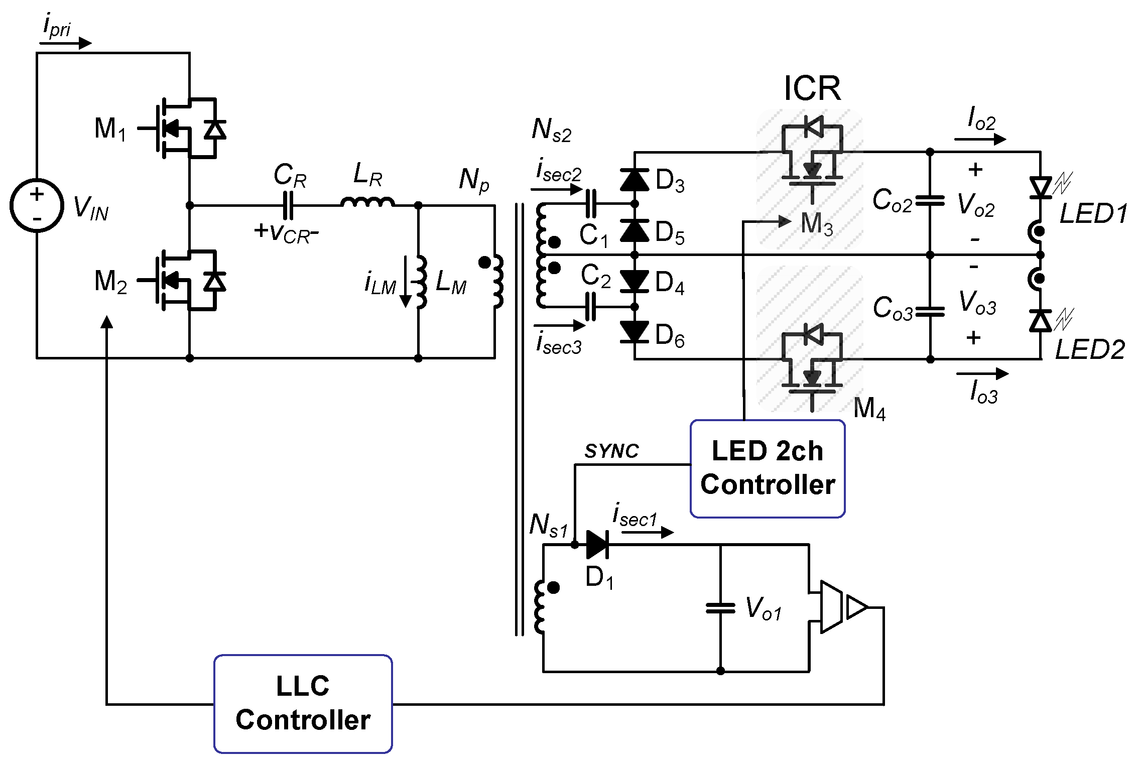
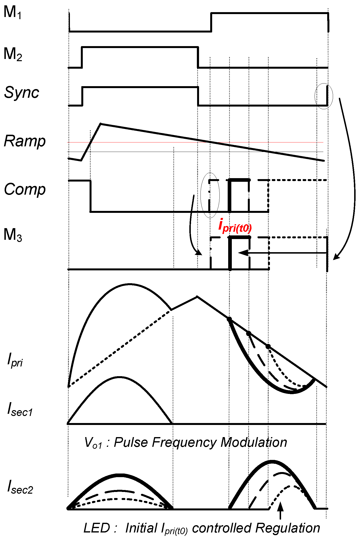
2.1. Control Method for Proposed Converter

The basic concept described in the paper is to supply the rectified secondary current directly driving the LED string and the regulated current to a single series transformer. As shown in Figure 2, the proposed post-regulator should be synchronized with the switching voltage of the secondary winding. Figure 3 shows the manner in which the proposed initial current control regulation is performed for one LED channel. The gating signal of the auxiliary switch is synchronized with the primary side switch to ensure zero voltage switching [12,13,14].
The output voltage Vo1 can be controlled by determining the switching frequencies of M1 and M2, as in a conventional LLC resonant converter [15,16,17,18]. However, io2 is controlled by the turn-on point of M3 when M2 is turned on. That is, although M2 is conducting and −vCR is applied to the primary side of the transformer, M3, which is turned off, prevents the input power from being transferred to the output side. At this time, D4 and D5 are turned on and charged to C1 and C2, respectively. Therefore, resonance does not occur between CR and LR, isec2 is maintained at zero, and the initial current Iini decreases with the slope of −vCR/(LR + LM). When M3 is turned on with M1 conducting, the secondary-side diode D3 is turned on, and simultaneously, the resonant current between CR and LR is transferred to the output side of the converter. At this point, in the case that M3 is turned on earlier, the resonant current ipri(t) is increased further, owing to the larger initial value Iini, which causes the output current io2 to increase. In contrast, the resonant current ipri(t) decreases more when M3 is turned on later.

2.2. Analysis of Operational Modes

The main waveforms are shown in Figure 4. The proposed converter operates in five modes [19] according to the conduction state of each switch (M1, M2, and M3), as shown in Figure 5.
For the expediency of mode analysis in a steady state, several assumptions are made, as follows.
(1)
The switch is ideal, except for the internal diode.
(2)
The transformer is ideal, except for the magnetizing inductance Lm and leakage inductance LR.
(3)
The output capacitors Co1 and Co2 are large enough to be considered as constant DC voltage sources Vo1 and Vo2, respectively.
(4)
The switching transition interval between M1 and M2 is small enough to be ignored.
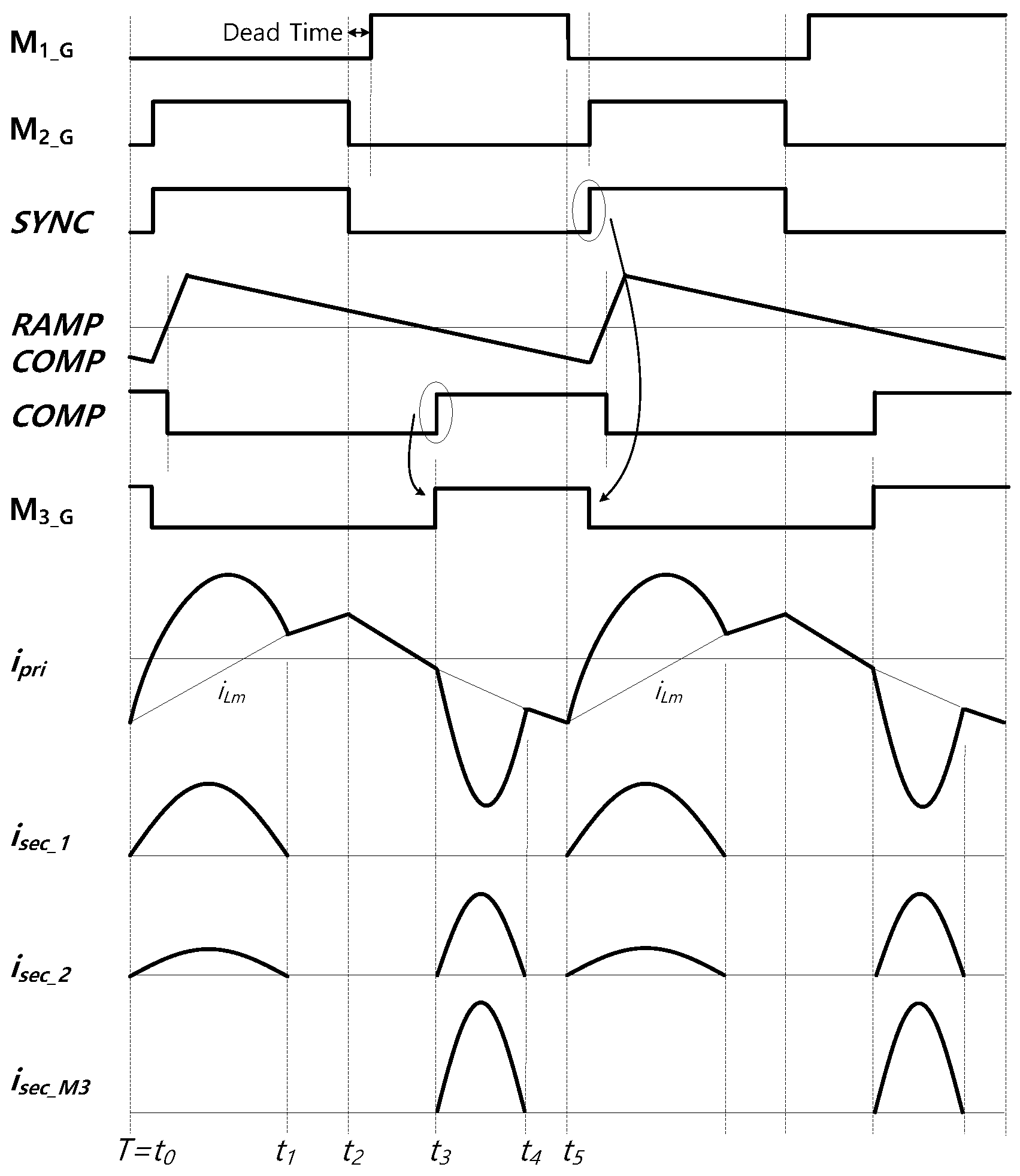
It is assumed that the switch M1 is conducting before t0 and that a transformer magnetizing current iLm flows through M1, as shown in Figure 4.
  • Mode 1 [t0t1]: This mode starts when M1 is turned off at t0. At this moment, the current of the resonant inductor LR is negative; it will flow through the body diode of M2, creating a zero-voltage switching (ZVS) condition for M2. The gating signal of M2 should be applied during this mode.
    When the current of the resonant inductor LR flows through the body diode of M2, Ipri starts to rise. As the voltage VIN–vCR across the primary side of the transformer is higher than the reflected output voltage (NP/NS1)Vo1, D1 is turned on.
    Concurrently, the transformer primary current ipri starts to increase, based on the resonance between CR and LR. The magnetic current iLm increases linearly as the reflected output voltage (NP/NS1)Vo1 is applied to Lm. Therefore, it does not participate in the resonance during this period. In this mode, the circuit operates as a series resonant converter (SRC), with a resonant inductor LR and resonant capacitor CR. This mode is terminated when the LR current is the same as the Lm current.
  • Mode 2 [t1t2]: When the transformer primary current ipri becomes equal to iLM and isec1 reaches zero at t1, Mode 2 begins. At this moment, D1 is blocked, and VIN–vCR is applied to LM + LR. The value of ipri is still increasing owing to the resonance between CR and LM + LR, as shown in Figure 5c, and the primary current ipri is still increasing, based on the resonance between CR and Lm + LR.
  • Mode 3 [t2t3]: When M2 is turned off and M1 is turned on at t2, Mode 3 begins. Although M1 is conducting and −vCR is applied to the primary side of the transformer, the turned off M3 prevents the input power from being transferred to the output side. Therefore, resonance does not occur between CR and LR, isec2 is maintained at zero, and the initial current Iini decreases with the slope of −vCR/(LR + Lm). The primary current ipri decreases in the same manner as the resonance between CR and LM + LR.
  • Mode 4 [t3t4]: When M3 is turned on at t3, Mode 4 starts, as shown in Figure 4. D3 is turned on because the voltage vCR is higher than the reflected output voltage (NP/NS2)Vo2. Concurrently, the primary current begins to decrease owing to the resonance between CR and LR. In addition, the reflected output voltage −(NP/NS2)Vo2 is applied to LM, causing the magnetizing current iLM to decrease linearly.
  • Mode 5 [t4t5]: Mode 5 begins when the primary current ipri becomes equal to the magnetizing current iLM, and the secondary current of the transformer, isec2, reaches zero at t4. At this moment, the primary current ipri is still decreasing owing to the resonance between CR and LM + LR, because D3 and D6 are blocked and −vCR is applied to LM + LR, as shown in Figure 5e. If only M3 and M4 are turned off after t5, M3 and M4 can be turned off to the Sync signal under the ZCS operation. This mode is terminated when M1 is switched off at t5. Then, the operations from t0 to t5 are repeated.

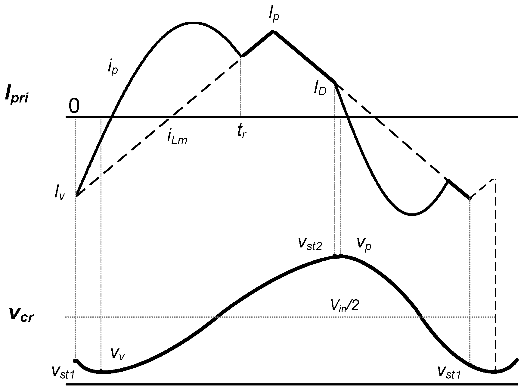
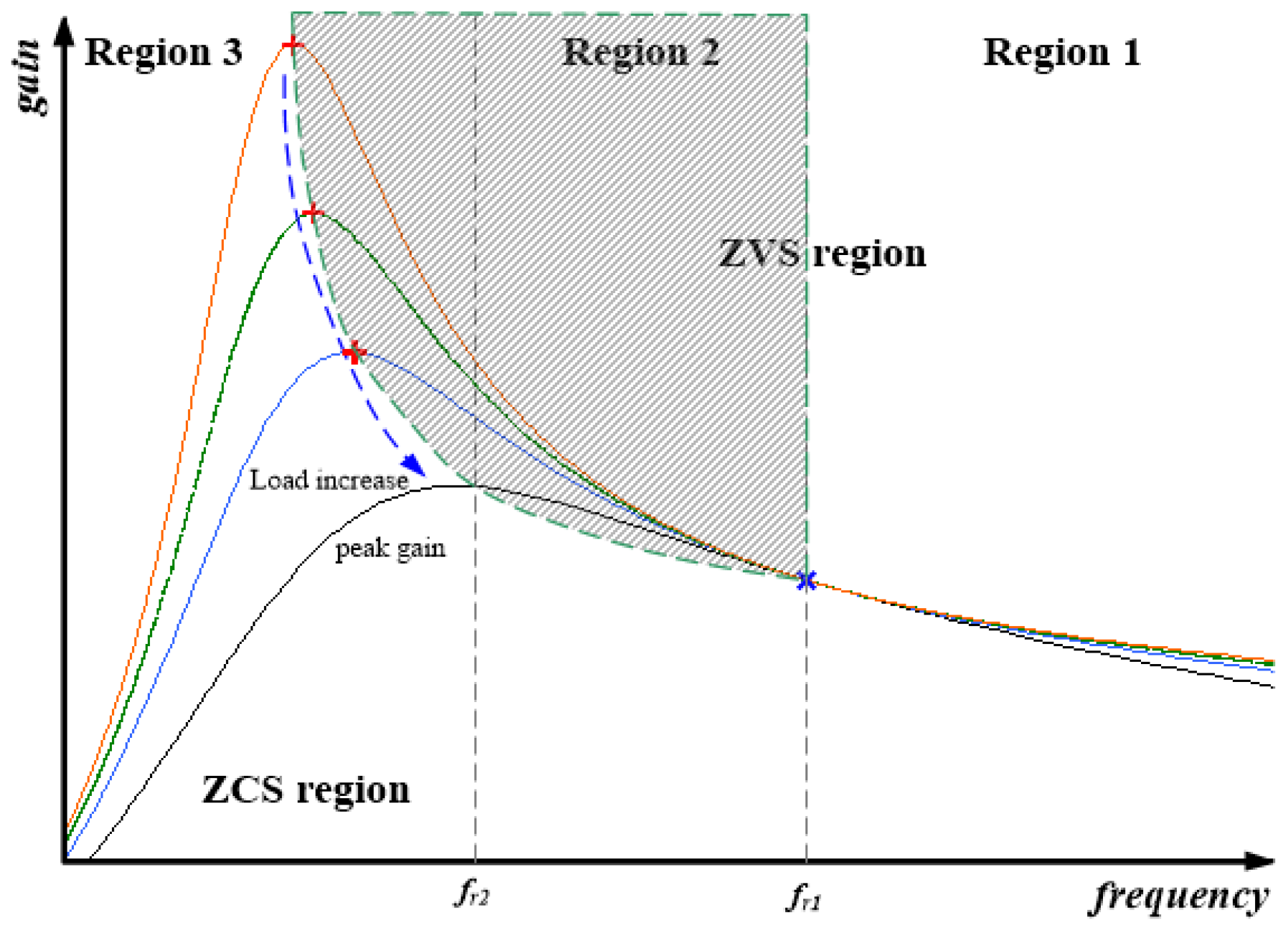
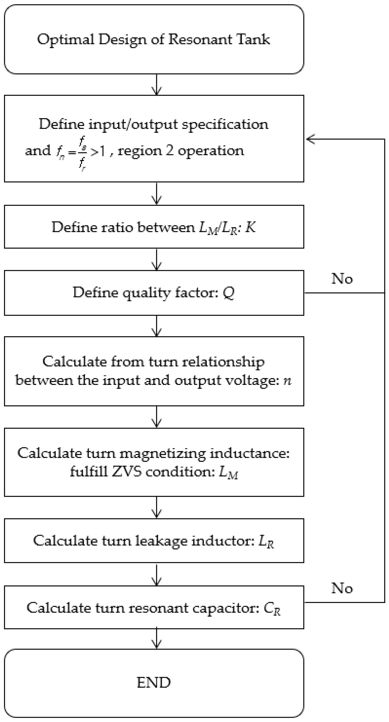
3. Analysis and Simplified Design Guidelines

3.1. Output Voltage Analysis

For convenience of analysis, it is assumed that the dead time between M1 and M2 is zero, and that iLM linearly increases or decreases with the slope of Vo1/n1LM orVo2/n2LM, respectively.
As shown in Figure 6, the steady-state offset current iLM through LM can be obtained as:
i L M = n 2 I o 2 n 1 I o 1
Here n1 = Ns1/Np and n2 = Ns2/Np, respectively.
From Equation (1), the values of Ip and Iv can be expressed as follows:
I p = ( n 2 I o 2 N 1 I o 1 ) + V o 1 T s 4 n 1 L M
I v = ( n 2 I o 2 N 1 I o 1 ) + V o 2 T s 4 n 2 L M
Here, Ts is the switching period.
Moreover, iLM1 and iLM2 can be obtained from Equations (4) and (5), as follows:
I v L M 1 ( t ) = V o 1 n 1 L M t + ( ( n 2 I o 2 N 1 I o 1 ) + V o 2 T s 4 n 2 L M )
I v L M 2 ( t ) = V o 2 n 2 L M t + ( ( n 2 I o 2 N 1 I o 1 ) + V o 1 T s 4 n 1 L M )
Furthermore, when M2 is conducting, the difference between ipri and iLM1 is transferred to the output side as isec1. Similarly, when M1 is conducting, the difference between ipri and iLM2 is transferred to the output side as isec2. From Equations (2), (6), and (7), isec1 during t0t1 and isec2 during t3t4 can be obtained as follows:
i sec 1 = 1 n 1 | i p r i i L M 1 | = I i n i 1 cos ω t + V c r i n i 1 V I N + V o 1 / n 1 L R / C R sin ω t { V o 1 n 1 L M t + ( ( n 2 I o 2 N 1 I o 1 ) + V o 2 T s 4 n 2 L M ) }
i sec 2 = 1 n 2 | i p r i i L M 2 | = I i n i 2 cos ω t + V c r i n i 2 V I N + V o 2 / n 2 L R / C R sin ω t { V o 2 n 2 L M t + ( ( n 2 I o 2 N 1 I o 1 ) + V o 1 T s 4 n 1 L M ) }
In the equations above, ω is the angular frequency.
Therefore, the output load currents Io1 and Io2 can be calculated from the mean values of isec1 and isec2, respectively, as follows:
I o 1 = 1 n 1 T s o t r I i n i 1 cos ϖ t + V c r i n i 1 V I N + V o 1 / n 1 L R / C R sin ϖ t { V o 1 n 1 L M t + ( ( n 2 I o 2 N 1 I o 1 ) + V o 2 T s 4 n 2 L M ) } d t = V o 1 R o 1
I o 2 = 1 n 2 T s o t r D T s I i n i 2 cos ϖ t + V c r i n i 2 V I N + V o 2 / n 2 L R / C R sin ϖ t { V o 2 n 2 L M t + ( ( n 2 I o 2 N 1 I o 1 ) + V o 2 T s 4 n 2 L M ) } d t = V o 2 R o 2
Here, D’ is the turn-off duty ratio of the switch M3.
From Equations (10) and (11), where trs = trD’Ts, the output voltages Vo1 and Vo2 can be obtained, as follows:
V o 1 = γ ( V c r i n i s V I N ) ( cos ϖ t r 1 ) ( n 1 T s R 01 β ω sin ω t r s γ n 1 ) ( cos ω t r s 1 ) + t 2 r 2 n 1 L M + α t r
V o 2 = γ ( V c r i n i s 2 V I N ) ( cos ω t r 1 ) ( n 2 T s R 02 β ω sin ω t r s γ n 2 ) ( cos ω t r s 1 ) + t 2 r 2 n 2 L M + β t r
Here, the variables α, β, γ are defined:
α = ( n 1 2 R o 2 n 2 2 R o 1 n 1 R o 1 R o 2 + T s 4 n 1 L M ) β = ( n 1 2 R o 2 n 2 2 R o 1 n 1 R o 1 R o 2 + ( 4 D 1 ) T s 4 n 1 L M ) γ = 1 ω C R L R

3.2. Simplified Design Guidelines

The design of resonant components such as LR, LM, and CR always involves a compromise between the maximum load variation, maximum allowable operating frequency deviation, maximum input voltage range, circulating energy in the resonant circuit, and short-circuit characteristics. The optimal operating point of the converter can be reached for a given input voltage and load resistance. Therefore, in practice, a converter is typically designed using operating conditions such as a high resonant frequency and maximum DC-link voltage. In the design of an LLC topology, it is crucial that the manufacturing tolerances of the inductors and capacitors are higher than those in standard productions.
(1)
Switching frequency (fs)
The switching frequency of the converter is determined based on the total losses of the switches and transformer. Generally, a higher switching frequency selection results in a lower magnetic flux; thus, the core size, as well as the core loss, can be reduced. However, a higher switching frequency also results in a higher AC loss on the winding of the transformer and a turn-off loss on the switches, reducing the converter efficiency. As a result, the selection of the switching frequency is a trade-off between these two effects. The trade-off depends on the power rating, type of semiconductor, and operating range of the converter.
(2)
Resonant tank frequency (fn)
One goal is to minimize the resistive losses in the duration of the circulating stages of Mode 2 and Mode 5, as shown in Figure 4. This can be achieved by setting the frequency ratio fn of the switching frequency (fs) to the resonant frequency of the resonant tank (fr) smaller than (but close to) unity.
f n = f s f r < 1
This frequency ratio is designed such that the converter can be operated at a switching frequency between fr2 and fr1, where fr2 and fr1 are determined by {(LM + LR) and CR} and {LR and CR}, respectively. This operating point is located in Region 2, as shown in Figure 7 [19].
In Figure 7, Region 1 is the SRC operation region. The converter operates in this region when the switching frequency is higher than fr1. The magnetizing inductance does not participate in the resonance, and a ZVS condition is naturally assured. Region 2 is the multi-resonant converter region. The load condition between fr1 and fr2 determines the operation of the converter under ZVS and zero current switching (ZCS) conditions.
In this region, the energy stored in the magnetic components triggers ZVS for the opposite Metal Oxide Semiconductor Field Effect Transistor (MOSFET). Region 3 is an overloaded region. In this area, the converter enters the ZCS mode. In general, the LLC resonant converter is designed to operate in Regions 1 and 2, owing to output regulation and ZVS operation. To ensure ZVS operation, the operating range of the converter should be above fr2. Therefore, LR and CR are chosen to be guaranteed under a heavy load. The selection of LM determines the switching frequency range and the MOSFET turn-off current. The smaller the value of LM, the narrower the operating range. However, the MOSFET turn-off current will be higher, increasing the switching loss.
(3)
Magnetizing inductance of the transformer (LM)
The ZVS operation of the MOSFETs and the ZCS operation of the output auxiliary switches are particularly important for the efficiency and optimal design of the LLC resonant converter. In Figure 6, the primary current is always negative at t0, ensuring that M2 operates under a ZVS condition. In addition, M1 always operates under the ZVS condition, owing to the positive Ip. Therefore, the ZVS condition of the two power switches depends on the magnetizing inductance LM and dead time duration tdt, as follows:
t d t > 2 V I N C d s I p _ min , t d t > 2 V I N C d s | I v _ min |
From Equation (6), the limitation of the magnetizing inductance can be derived as follows:
L M t d t 16 C s f s _ max
Here, tdt is the dead time and Cds is the equivalent capacitance of the MOSFETs.
The magnetizing inductor needs to be small enough to achieve the ZVS condition, and large enough to reduce the turn-off losses. Therefore, in an optimal design, LM should have the maximum value that meets the ZVS requirement.

3.3. Optimal Design of the LLC Resonant Converter

Figure 8 shows a flow chart for the optimal design of inductor-inductor-capacitor (LLC) resonance tank. The following is the step-by-step design guide line.
Step 1. Refer to the above “(1) Switching frequency (fs) (2) Resonant tank frequency (fn)” and select the switching frequency range. The converter is designed to operate in Region 2 at high and low input voltages to minimize switching loss due to hard-switching. For ZCS operation of the secondary-side output rectifier, switching frequency fs shall be lower than resonant frequency fr1. The limit of fr is defined as follows.
f r = 1 2 π L R C R
Step 2. When Q decreases (load decrease) higher peak gains are obtained. In addition, the important factor determining peak gain is the ratio between LM/LR. The ratio between LM/LR and quality factor is defined as follows.
K = L M L R ,   Q = L R / C R R a c
Step 3. The turn ratio n should be calculated from the relationship between the input and output voltages.
n V i n / 2 V o 1 + V f
Step 4. The magnetizing inductance needs to be small enough to achieve the ZVS condition, and large enough to reduce the turn-off losses. From Equation (14), the limitation of the magnetizing inductance can be derived as:
L M t d t 16 C s f s _ max
Step 5. The leakage inductance can be calculated from Equation (15) and as follows:
L R = Q R a c 2 π f r
Here, n is transformer turns ratio and Rac is AC equivalent load resistance, R a c = 8 n 2 π 2 R o , n = N P N s .
Step 7. The resonant capacitor can be calculated from Equation (15) and as follows:
C R = 1 2 π f r Q R a c

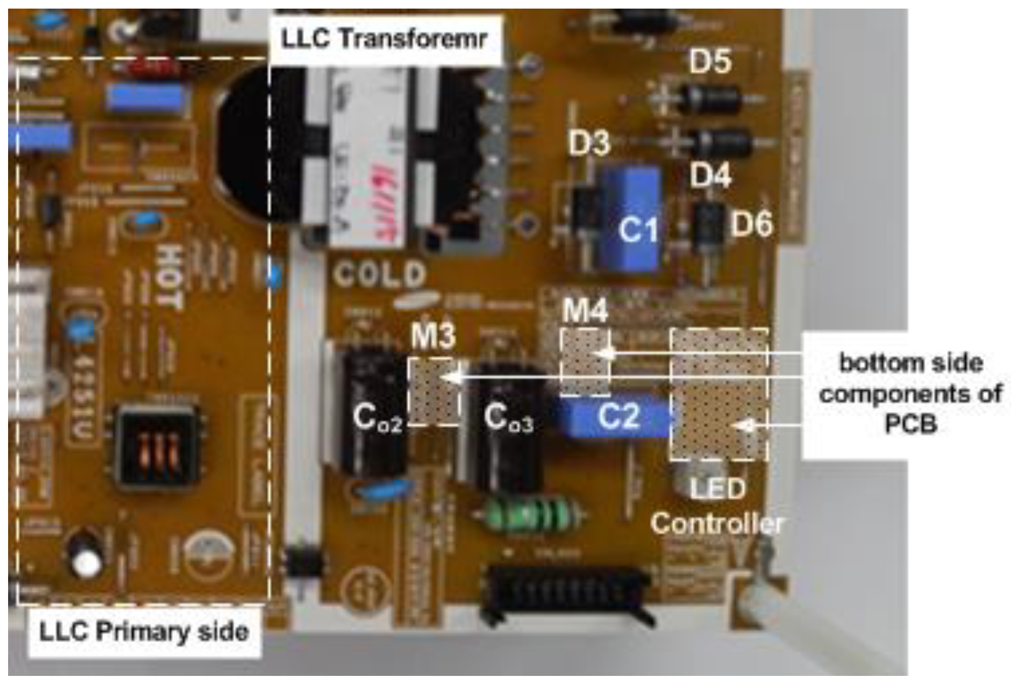
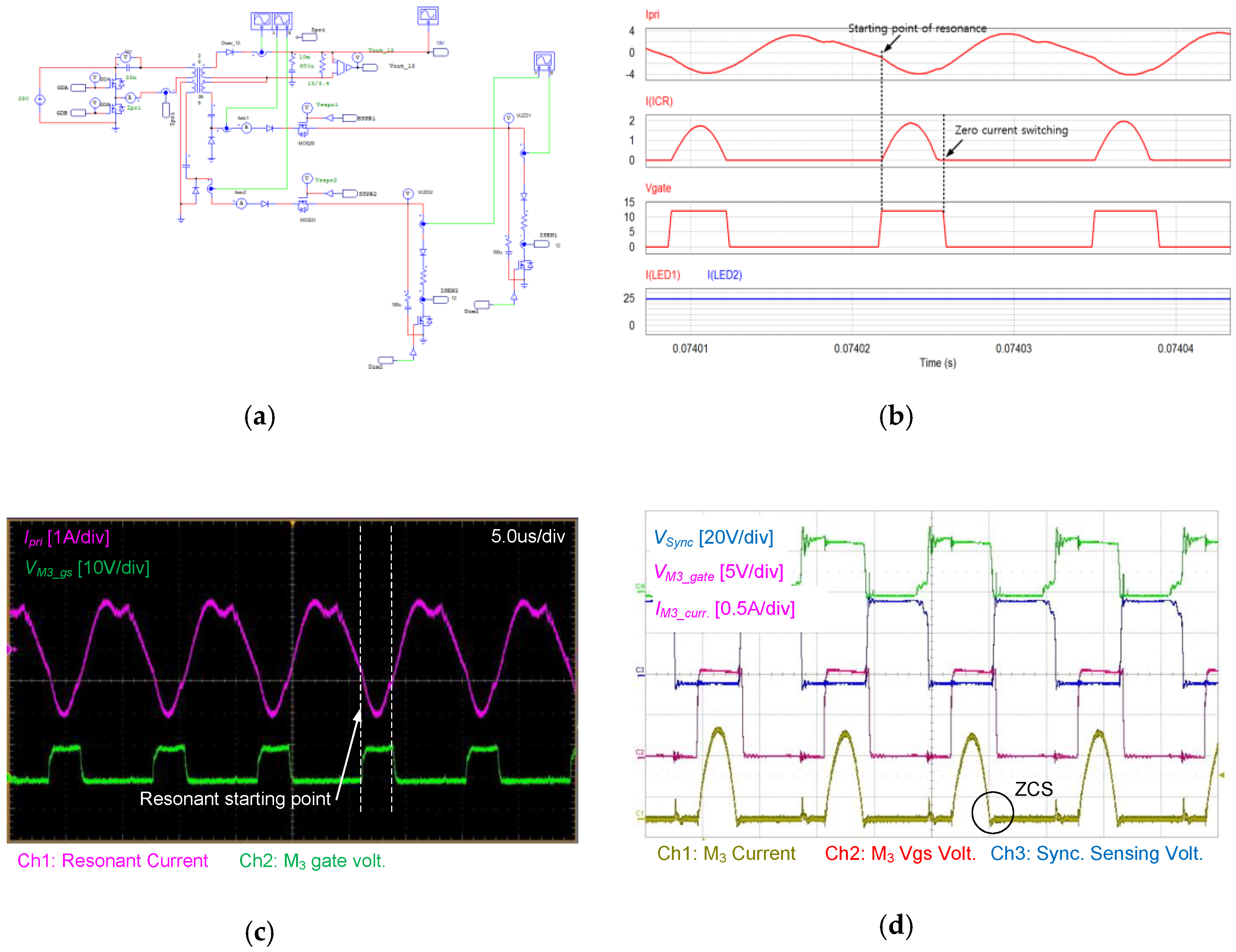
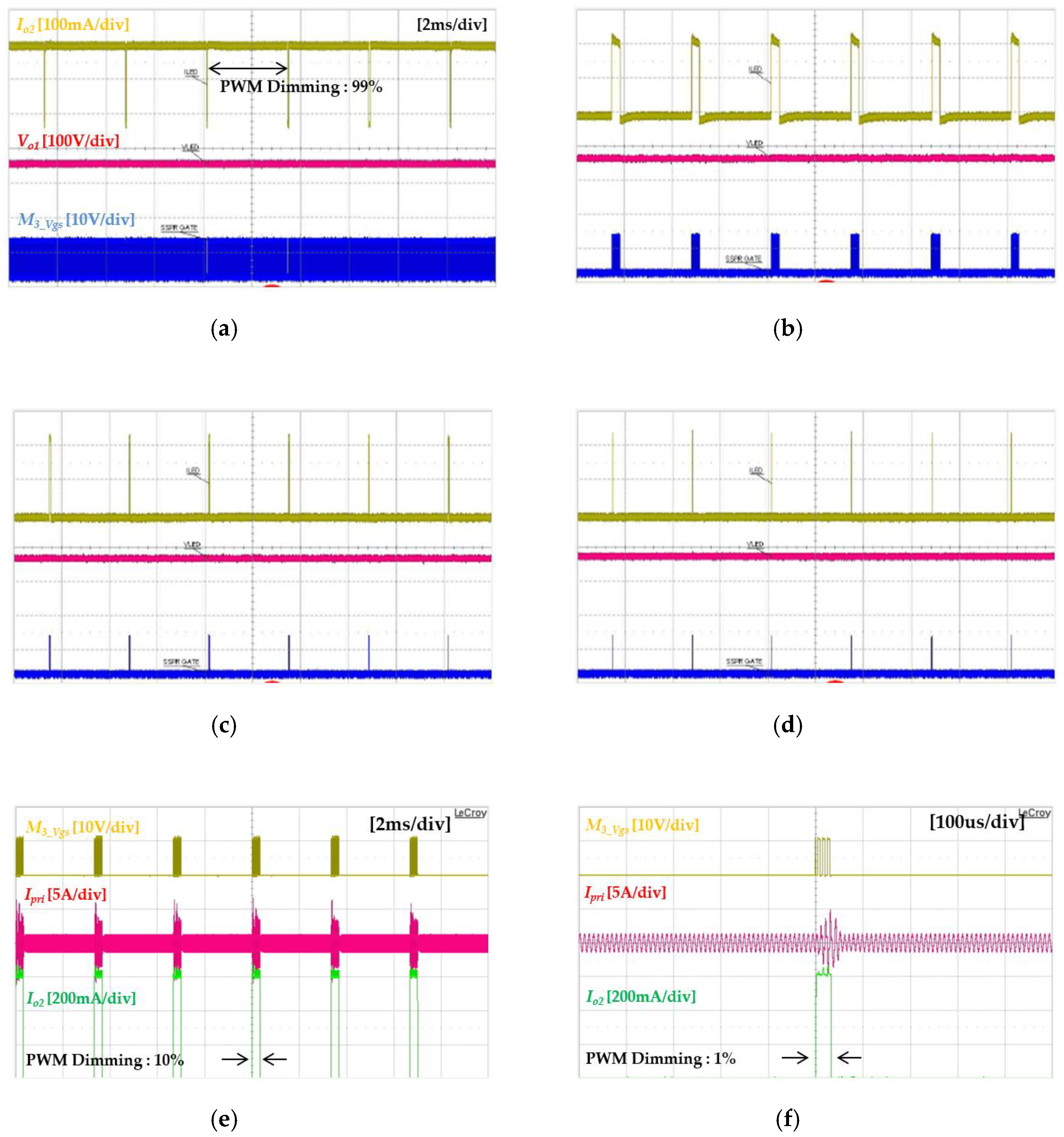
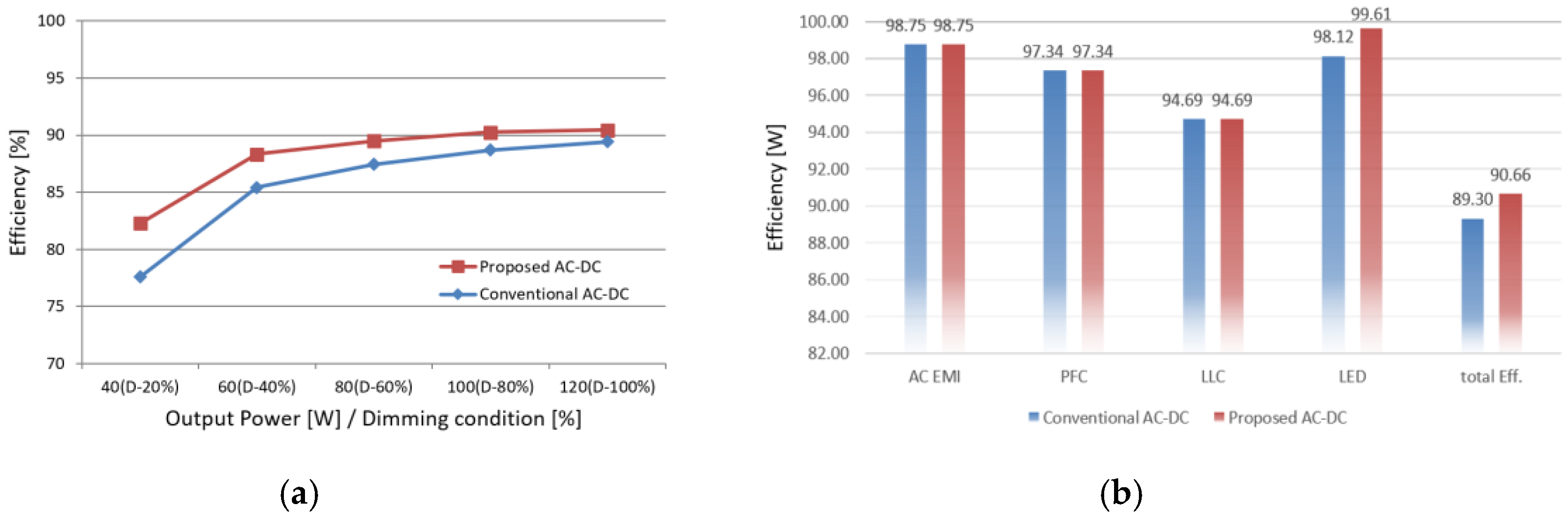
4. Experimental Results

To verify the feasibility of the proposed converter, a prototype of a 120 W output power converter for LED 3D TVs is implemented. The prototype of the proposed LED driver is shown in Figure 9.
Table 1 shows the design specifications and circuit parameters for the prototype. Table 2 shows a comparison between the conventional and proposed circuits, in terms of the number of components. As shown in Table 2, the proposed converter has fewer components than the number of components in the conventional converter owing to the absence of the additional non-isolated DC-DC converter.
Figure 10 shows the ZCS operating waveforms of the proposed converter; when M3 is turned on, the resonant current of the primary side starts flowing. It is clear that ZCS is ensured, based on the zero current at the end of the ICR switching.
Figure 11 shows the experimental waveforms at 2D (99%, 10%, 1%, and 0.2%) and 3D (10% and 1%) dimming ratios. As shown in Figure 11, the LED current becomes zero for the low dimming signal, and it is exactly controlled to be 2D_210 mA and 3D_630 mA for the high dimming signal. Moreover, although the proposed LED driver comprises only a few components, the current through the LED array is well-controlled and balanced according to all of the dimming ratios.
Based on Table 1, Figure 12 shows the total efficiency of the power system from AC to the final LED backlight (AC EMI + PFC + DC/DC + LED backlight driver) and the efficiency of each stage is also compared. Efficiency measurements are efficiency data according to LED dimming conditions as shown in Figure 11. This is a measure of operating from dark to full brightness on a TV screen. Assuming that the components not specified in Figure 12 have similar power consumptions, the proposed driver shows a lower consumption by approximately 1.74 W power loss than the conventional driver.
Probably of the most importance is the high efficiency with this LLC topology that allows slim power supply designs. LED string current control is achieved using the LLC resonant half bridge topology in current mode control. Typical efficiency for the proposed converter in TV application is shown in Figure 12; the total efficiency from AC to backlight can be achieved by more than 90% with this architecture.

5. Conclusions

In this paper, optimal design of a multi-output LLC resonant converter with an independently regulated synchronous single-switched power-regulator is proposed. As an isolated DC-DC converter and LED drivers are integrated into one power stage in the proposed LED driver system, it consists of two cascaded power stages. The proposed post-regulator requires only one auxiliary switch, in contrast with a bulky and expensive non-isolated DC-DC converter
Through the analysis of the control method for the proposed converter, the simplified design guidelines and magnetizing inductance are designed to obtain soft switching capability. The proposed driver system features a relatively low cost, simple structure, high efficiency, and high power density. In addition, it can ensure the ZVS operation of power switches and the ZCS operation of output auxiliary switches along the entire load range. It has highly desirable advantages, such as reduced switching losses and heat generation.
Finally, through the experimental results it can be seen that very fast LED rise and fall currents can be achieved with this control scheme that allow excellent linearity performance under any dimming conditions. The proposed converter is simple and achieves excellent dimming current control between multiple outputs, and the highest AC to backlight efficiency. The PSIM simulation and experimental results using the prototype converter verified the validity of the proposed architecture.

Author Contributions

Conceptualization, S.G.P. and B.K.L.; methodology, S.G.P. and J.S.K.; software, S.G.P.; validation, S.G.P. and J.S.K.; formal analysis, S.G.P.; investigation, S.G.P.; resources, S.G.P. and B.K.L.; data curation, S.G.P. and J.S.K.; writing—original draft preparation, S.G.P.; writing—review and editing, J.S.K.; visualization, S.G.P.; supervision, B.K.L.; project administration, B.K.L. All authors have read and agreed to the published version of the manuscript.

Funding

This research received no external funding.

Conflicts of Interest

The authors declare no conflict of interest.

References

  1. Qu, X.; Wong, S.-C.; Tse, C.K. A current balancing scheme with high luminous efficiency for high power LED lighting. In Proceedings of the IECON 2013-39th Annual Conference of the IEEE Industrial Electronics Society, Vienna, Austria, 10–13 November 2013. [Google Scholar]
  2. Liu, J.; Sun, W.; Zeng, J. Precise current sharing control for multi-channel LED driver based on switch-controlled capacitor. IET Power Electron. 2017, 10, 357–367. [Google Scholar] [CrossRef]
  3. Chen, Y.; Wu, X.; Qian, Z. Analysis and design considerations of LLCC resonant dc–dc converter with precise current sharing for two-channel LED driver. In Proceedings of the 2011 IEEE Energy Conversion Congress and Exposition, Phoenix, AZ, USA, 17–22 September 2011; pp. 2771–2776. [Google Scholar]
  4. Raghavendra, K.V.G.; Zeb, K.; Muthusamy, A.; Krishna, T.N.V.; Prabhudeva Kumar, S.V.S.V.; Kim, D.-H.; Kim, M.-S.; Cho, H.-G.; Kim, H.-J. A comprehensive review of DC–DC converter topologies and modulation strategies with recent advances in solar photovoltaic systems. Electronics 2019, 9, 31. [Google Scholar] [CrossRef] [Green Version]
  5. Park, S.-G.; Ryu, S.-H.; Cho, K.-S.; Lee, B.-K. An improved single switched post regulator for multiple output isolated converters. In Proceedings of the 2015 9th International Conference on Power Electronics and ECCE Asia (ICPE-ECCE Asia), Seoul, Korea, 1–5 June 2015; pp. 2403–2408. [Google Scholar]
  6. Vinoth Kumar, K.; Shankar, A.; Renius, J.S.; Guru, R.; Nair, S.L.; Viswanathan, K. The FHA analysis of dual-bridge LLC type resonant converter arnold fredderics. Int. J. Power Electron. Drive Syst. (IJPEDS) 2014, 4, 538–546. [Google Scholar]
  7. Lo, Y.K.; Yen, S.C.; Song, T.H. Analysis and design of a double-output series- resonant DC-DC converter. IEEE Trans. Power Electron. 2007, 22, 952–959. [Google Scholar] [CrossRef]
  8. Gu, Y.; Hang, L.; Chen, U.; Lu, Z.; Qian, Z.; Li, J. A simple structure of LLC resonant DC-DC converter for multi-output applications. In Proceedings of the 2005 20th Annual Meeting of Applied Power Electronics Conference, Austin, TX, USA, 6–10 March 2005; Volume 3, pp. 1485–1490. [Google Scholar]
  9. Jovanović, M.M.; Irving, B.T. Efficiency optimization of LLC resonant converters operating in wide input-and/or output-voltage range by on-the-fly topology-morphing control. In Proceedings of the IEEE Applied Power Electronics Conference (APEC), Charlotte, NC, USA, 15–19 March 2015. [Google Scholar]
  10. Chandrasekar, B.; Samuel Rajesh Babu, R. A review on LLC resonant converter. In Proceedings of the International Conference on Computation of Power, Energy Information and Communication (ICCPEIC), Chennai, India, 20–21 April 2016. [Google Scholar]
  11. Kim, C.-E.; Moon, G.-W.; Lee, J.-Y.; Park, K.-B. New Multi-output LLC resonant converter for high efficiency and low cost PDP power module. In Proceedings of the 2006 37th IEEE Power Electronics Specialists Conference, Jeju, Korea, 18–22 June 2006; pp. 1–7. [Google Scholar]
  12. Hang, L.-J.; Gu, Y.-L.; Lu, Z.-Y.; Qian, Z.-M. Multi-output LLC resonant converter with symmetrical auxiliary output structure. In Proceedings of the INTELEC 06-Twenty-Eighth International Telecommunications Energy Conference, Providence, RI, USA, 10–14 September 2006; pp. 1–5. [Google Scholar]
  13. Lin, Y.-L.; Liu, K.H. A new synchronous-switch post regulator for multi-output forward converters. In Proceedings of the Fifth Annual Proceedings on Applied Power Electronics Conference and Exposition, Los Angeles, CA, USA, 11–16 March 1990; pp. 693–696. [Google Scholar]
  14. Zhang, J.; Liao, J.; Wang, J.; Qian, Z. A current-driving synchronous rectifier for an LLC resonant converter with voltage-doubler rectifier structure. IEEE Trans. Power Electron. 2012, 27, 1894–1904. [Google Scholar] [CrossRef]
  15. Qian, Q.; Yu, J.; Su, C.; Sun, W.; Lu, W. A LLC resonant converter with dual resonant frequency for high light load efficiency. Int. J. Electron. 2017, 104, 2033–2047. [Google Scholar] [CrossRef]
  16. Luo, J.; Wang, J.; Fang, Z.; Shao, J.; Li, J. Optimal design of a high efficiency LLC resonant converter with a narrow frequency range for voltage regulation. Energies 2018, 11, 1124. [Google Scholar] [CrossRef] [Green Version]
  17. Park, H.P.; Jung, J.H. PWM and PFM hybrid control method for LLC resonant converters in high switching frequency operation. IEEE Trans. Ind. Electron. 2017, 64, 253–263. [Google Scholar] [CrossRef]
  18. Su, B.; Wen, H.; Zhang, J.; Lu, Z. A soft-switching post regulator for multi-outputs dual forward dc/dc converter with tight output voltage regulation. IET Power Electron. 2013, 6, 1067–1077. [Google Scholar] [CrossRef]
  19. Fang, X.; Hu, H.; John Shen, Z.; Batarseh, I. Operation mode analysis and peak gain approximation of the LLC resonant converter. IEEE Trans. Power Electron. 2012, 27, 1985–1995. [Google Scholar] [CrossRef]
Figure 1. Conventional front-end AC–DC power supply: (a) three stages of power system and inverter stage on the primary side of the conventional converter; (b) schematic of conventional LED driving.
Energies 13 04341 g001
Figure 2. Proposed converter schematic.
Energies 13 04341 g002
Figure 3. Control method of proposed converter.
Energies 13 04341 g003
Figure 4. Key waveforms of proposed converter.
Energies 13 04341 g004
Figure 5. Operation modes of the proposed converter: (a) Mode 1; (b) Mode 2; (c) Mode 3; (d) Mode 4; and (e) Mode 5.
Energies 13 04341 g005
Figure 6. Waveforms of resonant current ipri(t) and voltage vCR(t) for steady state.
Energies 13 04341 g006
Figure 7. DC gain characteristics under load variations.
Energies 13 04341 g007
Figure 8. Flowchart for optimal design of inductor–inductor–capacitor (LLC) resonance tank.
Energies 13 04341 g008
Figure 9. The prototype of the proposed LED driver.
Energies 13 04341 g009
Figure 10. Computer simulation and experimental waveform of M3: (a) PSIM simulation circuit; (b) PSIM simulation graph; (c) resonance current on primary side converted to output side; and (d) zero current switching (ZCS) operating waveforms of the proposed converter.
Energies 13 04341 g010
Figure 11. Experimental waveforms according to LED 2D/3D dimming: (a) 2D pulse width modulation (PWM) dimming: 99%; (b) 2D PWM dimming: 10%; (c) 2D PWM dimming: 1%; (d) 2D PWM dimming: 0.2%; (e) 3D PWM dimming: 10%; and (f) 3D PWM dimming: 1%.
Energies 13 04341 g011
Figure 12. Measured total efficiency (AC to LED backlight driver): (a) comparison of efficiency by LED dimming conditions; (b) comparison of efficiency by each Stage (AC EMI + PFC + LLC + LED backlight).
Energies 13 04341 g012
Table 1. Design and circuit specification for power system.
Input Voltage, VINAC90–264V
Vvisual and Vamp12.8 V/5.4 A
LED Output (2CH)2D Mode_100V/240 mA
3D Mode_122V/630 mA
Output Power, Po,max120 W
Trans Turn Ratio, NP:NS1:NS239:2:32
Resonant Capacitor, Cr33 nF
Leakage Inductance, Lr94 uH
Magnetizing inductance, LM470 uH
LLC Resonant ControllerFA6A00N, Fuji Electric, Japan
Table 2. Comparisons between conventional and proposed converters (2CH).
ItemConventional CircuitProposed Circuit
Rectifier Diode4EASDURF1030 (TO-220)4EASF38G (DO-201A)
Heat Sink1EA60 mm × 30 mm × 9 mm
Power Switch2EAAOD9N25 (D-PAK)2EAAOD5N40 (D-PAK)
Freewheeling Diode2EAMUR460 (DO-201A)
Elec. Capacitor2EA68 uF/160 V
2EA33 uF/200 V2EA47 uF/200 V
Film Capacitor2EA100 nF/330 V
Inductor2EAEFD2020

