2. Experimental Procedures
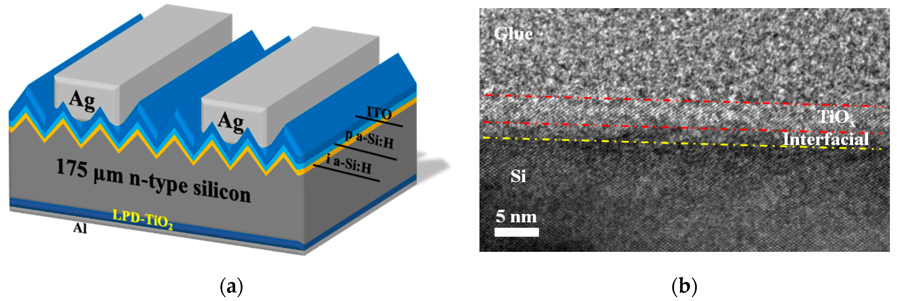
To fabricate the proposed solar cell, an n-type, 175 μm thick surface polished crystalline (100) silicon wafer (0.5–1 Ω-cm) was used as substrate. Prior to deposition, the Si substrate was textured in a potassium hydroxide (KOH) solution and etched in an etchant solution (HF:H
2O = 1:10) for 30 sec to remove surface damage and then rinsed with deionized water. After cleaning, a thin layer of intrinsic a-Si:H (5 nm) and B-doped a-Si:H (20 nm) are deposited sequentially by plasma-enhanced chemical vapor deposition (13.56 MHz). A 80 nm thick indium-tin oxide (ITO) transparent conductor was then deposited by sputtering. After that, the front surface was passivated with photoresist for rear-side TiO
x deposition. The TiO
x was deposited in 8, 16, and 25 nm thicknesses by a LPD method, details of which were published previously [
2,
3]. (NH
4)
2TiF
6 solution and H
3BO
3 were used as precursors. To ensure a saturated concentration of TiO
x, TiO
x powders were added to the precursor. The deposition temperature was maintained at 40 °C. The concentrations of (NH
4)
2TiF
6 and H
3BO
3 were 0.2 M and 0.6 M, respectively, in deionized water. The growth of TiO
2 consists of two equilibrium reactions. In the first step, the TiF ligand interacts with H
2O to form a titanium hydroxyl complex and HF (Equation (1)). The titanium hydroxyl complex is further transformed into TiO
x through a dehydration reaction. To maintain the continuous growth of TiO
x, the first equation should work forward by reducing the concentration of F ion simultaneously. This was achieved by the reaction of H
3BO
3 with HF in the second step (Equation (2)) [
10,
11]:
In this step, the chemical reaction consumes uncoordinated F to form stable BF
4− ions. Therefore, the consumption of the HF drives the chemical reaction represented in the Equation (1) toward TiO
x deposition on the substrate by dissolving supersaturated TiO
2 powder in the solution, in order to balance the chemical reaction. After TiO
x deposition, the photoresist was removed. The front (Ag~100 nm) and back contact (Al~200 nm) were deposited sequentially by a thermal evaporator through a shadow mask. The schematic diagram of the resulting solar cell device is shown in
Figure 1a. To analyse the device, the dark current density voltage (I-V) characteristics were measured by a B2912A semiconductor parameter analyzer (Agilent, Santa Clara, CA, USA) on a probe station. The photovoltaic characteristics were measured by a calibrated solar simulator under AM1.5 G (100 mW/cm
2) conditions. A QE-3000 system (Titan Electro-Optics, Taipei, Taiwan) was used to obtain external quantum efficiency (EQE). To study the material properties, a transmission electron microscope (TEM, model JEM-2100F, JEOL, Tokyo, Japan) was used to explore the TiO
x/Si interfaces. X-ray Photoelectron Spectroscopy (XPS, model PHI 5000 Versa Probe, ULVAC-PHI, Kanagawa, Japan) was used to understand the microstructure of TiO
x on Si. The lifetime was measured by a WCT-120 system (Sinton, Boulder, CO, USA) in quasi-steady-state photoconductance mode. The surface recombination velocity was calculated from the obtained lifetime.
3. Results and Discussions
A TEM image of the TiO
x/Si interface is shown in
Figure 1b. To grow a thin TiO
x layer, the growth rate is the key factor in the LPD process. The growth rate was determined by the thickness measurement on a thicker TiO
x by SEM. The TiO
x was then grown to the designed thickness by controlling the time in the LPD process. In
Figure 1b, the designed thickness is 5 nm. From the figure, the interfacial and TiO
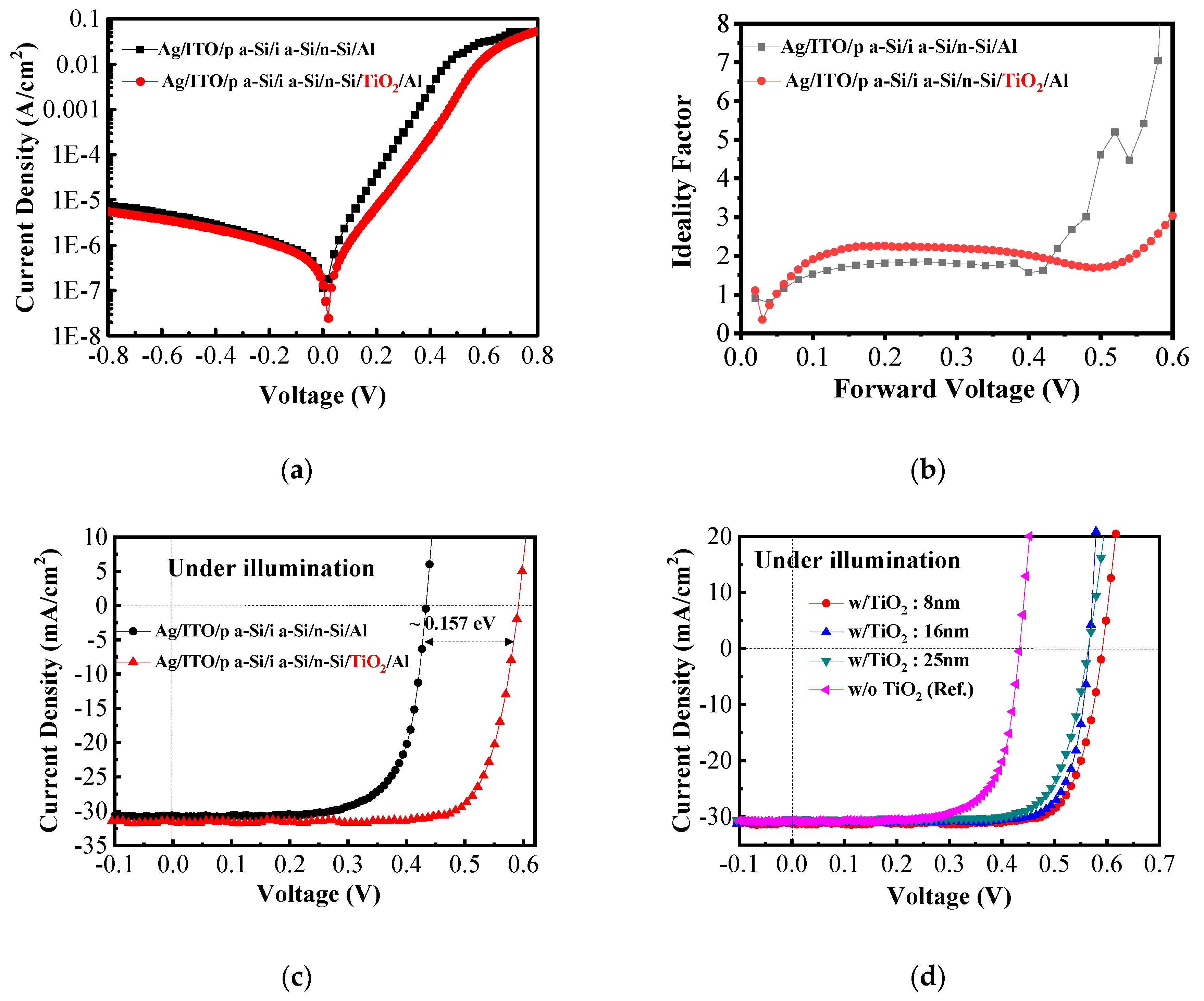
x layers are approximately 1 and 4 nm thick, as indicated. The measured thickness is consistent with the designed thickness, therefore, the thickness used in the device indicates matches the design thickness. The dark and photo-current density to voltage characteristics (J-V) are illustrated in
Figure 2a,c, respectively. Without solar light illumination, both solar cell devices with and without a TiO
x rear contact layer exhibit normal pn-junction diode behavior. The solar cell without TiO
x rear contact layer exhibits a higher current density for the same applied voltage. This implies the carriers are injected into device much easier without a TiO
x rear contact layer, however, the ease of injection also indicates the possibility of a smaller open-circuit voltage (
Voc), in which the
Voc is determined as the voltage at which the solar generation current and the injected current are balanced. The ideality factor, n, of both devices was calculated and is shown in
Figure 2b by the following pn-junction diode equations, as shown in Equation (3):
in which
J is the diode current,
J0 is the reverse saturation current density,
q is the electric charge of electron, k is the Boltzman constant,
T is the absolute temperature,
V is the applied voltage and the
n is the ideality factor. The term
n generally accounts for recombination at either the bulk or junctions, the heterointerfaces, and contact resistance under forward-biased conditions [
12]. The calculated ideality factor for a solar cell without a TiO
x rear contact layer is approximately 1.73 at a voltage smaller than 0.45 V and it increases rapidly after 0.45 V. In comparison, the solar cell with a 8 nm thick TiO
x rear contact layer exhibits a higher ideality factor, approximately 2.3, at voltages smaller than 0.55 V and a slight increase after this voltage. Since the bulk and the front contacts are identical for both solar cells, the difference in ideality factor must be caused by the rear contact, either from rear interface recombination or due to the interfacial barrier provided by TiO
x. The rapidly increased ideality factor at voltages higher than 0.45 V indicates a high voltage-drop in this region that may be attributed to high interfacial states for recombination in solar cells without a TiO
x rear contact layer. This could be clarified by the reverse saturation current,
J0, under reversed biased conditions, in which the
J0 contains information of the generation and recombination processes in the entire device. The reverse saturation current density,
J0, for a reference device (without TiO
x) is 1.1 × 10
−7 A/cm
2, and it is 2.5 × 10
−8 A/cm
2 for a device with a TiO
x rear contact layer. The solar cell device with TiO
x exhibits approximately a 4.4-fold reduction. These findings indicate that insertion of a thin layer of TiO
x may passivate the density of states of Si on the rear surface and improve the electrical contact behavior.
The photocurrent–voltage characteristics of the TiO
x and referenced solar cells are illustrated in
Figure 2c. The short-circuit current density (
Jsc), fill factor (FF) and open-circuit voltage (
Voc) of a solar cell with an 8 nm TiO
x rear interfacial layer are 31.5 mA/cm
2, 0.778, and 0.6 V, respectively. As a consequence, a power conversion efficiency (PCE) of 14.70% is achieved. Without a TiO
x rear contact, the values of those solar cell performance indicators are 30.7 mA/cm
2, 0.716, and 0.43 V, yielding an PCE of 9.57%. With the increased thickness of TiO
x (16 and 25 nm), the
Voc of devices decreased slightly, as compared to the solar cell device with a 8 nm thick TiO
x rear contact layer. The PCE was reduced slightly to 13.81 and 12.96%, respectively. The details of the
Voc,
Jsc, FF, PCE, series resistance (Rs) and shunt resistance (Rsh) for the solar cell devices are listed in
Table 1.
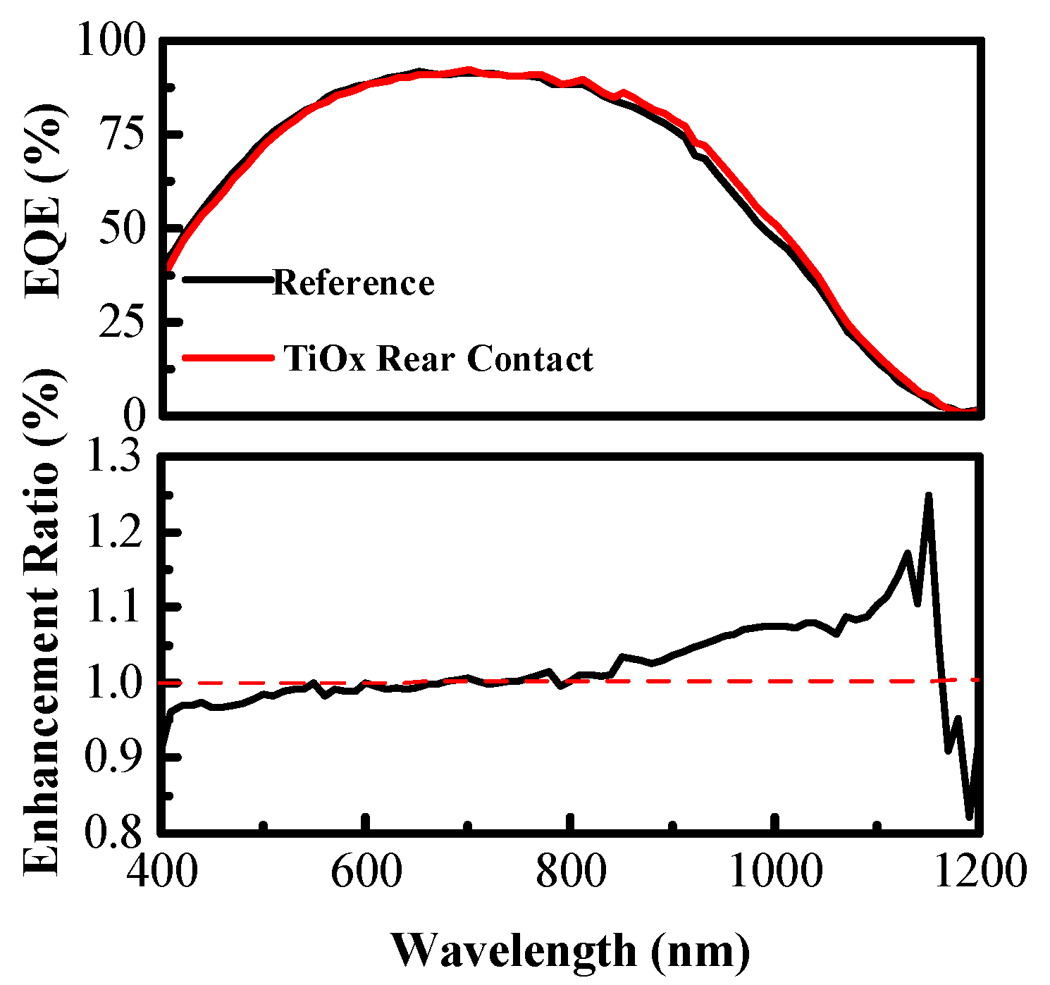
The enhancement in the
Voc for the TiO
x device is consistent with the higher ideality factor at forward-biased and the low recombination current density under reverse-biased conditions given by the following expression:
According to this equation, a high ideality factor and low recombination current density will result in a high
Voc if the photocurrent density remains constant. In contrast to
Voc, the
Jsc is similar for devices with and without TiO
x. They show only a slight difference, which is 0.7 mA/cm
2. The EQE for these two devices was taken at wavelengths from 400 to 1200 nm to understand the origin of the
Jsc enhancement, as shown in
Figure 3. The EQE for both devices are almost identical before 800 nm. After this wavelength, the device with TiO
x shows a slight enhancement. The enhancement ratio was calculated and is displayed in the lower part of
Figure 3. The enhancement is increased around 20% at wavelengths near 1100 nm. Usually long wavelength incident light can reach the rear side of a Si solar cell because of the low absorption coefficient at these wavelengths. Therefore, the enhancement in the EQE is attributed to the formation of TiO
x at the rear contact that passivates the interfaces. The microstructure of the TiO
x and Si interface will be discussed later using an XPS investigation. In addition to the interface passivation, the valence band edge of the TiO
x samples are higher than the edge of the valence band of the Si from our previous study, as the TiO
x will repel photogenerated holes back to the front contact, which increases the
Jsc and EQE.
Figure 4a depicts the O
1s and Si
2p core-level microstructure of the TiO
x obtained according to the XPS results. The O
1s spectrum exhibits three peaks after deconvolution, which correspond to TiO
2 (530.7 eV), oxygen deficient TiO
x (531.4 eV) and SiO
x (532.5 eV) [
13,
14,
15]. The Si-bonded O signal covers a broad energy range, that overlapps with the oxygen-deficient TiO
x signal, indicating the existence of oxygen deficient SiO
x and cross-bonding, such as Si-O-Ti. The Si 2p signal has two peaks, corresponding to Si (99 eV) and Si-O (102 eV), respectively [
16]. The appearance of Si-O bonding reveals a small amounts of silicon oxide exists either in the TiO
x or at the Si surface. The formation of SiO
x is a natural result in the LPD process. Water will react with the Si surface to form the oxide naturally. The HF will further dissolve SiO
2 into solution by etching. Finally, the dissolved SiO
2 and TiO
2 will regrow on the native oxide to form a layer comprising SiO
x, TiO
x and TiO
2.
The reduction in the dark current density provides evidence of improved junction quality. The formation of the SiO
x between Si and TiO
x could passivate the interfaces reducing the recombination. The physical evidence is the reduction of the surface recombination velocity (S). The SRV could be derived by the minority carrier lifetime (
τ). The relationship of S and
τ could be expressed by the following equation [
17,
18]:
in which the
τ is the minority carrier lifetime by measurement,
τb is the averaged bulk lifetime, S is the surface recombination velocity to be calculated, and W is the wafer thickness. The minority carrier lifetime for the bare-Si (with native oxide) and TiO
x-grown Si are indicated at
Figure 4b. The bare-Si and TiO
x-grown Si had average lifetimes of 16.8 and 40 μs, respectively. To calculate the S, the bulk lifetime was assumed to be 19 ms [
19]. The S values were 625 and 1488 cm/s for TiO
x and native oxide grown Si surface, respectively, by calculation. The TiO
x exhibits a 2.4-fold reduction of the surface recombination velocity compared to native oxide on Si. As a consequence, the TiO
x/Si has better passivation ability than native oxide.
The band alignments of the proposed device structure are plotted at
Figure 5a,b for the heterojunction (HJ) solar cell with and without a TiO
x rear contact layer, respectively. The conduction band edge (E
C) and valence band edge (E
V), for the Si (100) are 4.01 eV and 5.17 eV below the vacuum level, respectively. The Fermi energy (E
F) of the n-type Si is calculated according to the doping concentration (resistivity ~0.5 Ω-cm), which is 4.22 eV. The titanium oxide with empty and filled band edges at 4 eV and 7.2 eV below the vacuum level, respectively. Furthermore, the Fermi energy of the LPD-TiO
x layer is 4.2 eV [
3]. The conduction band and valence edges are 3.9~4.0 and 5.6~5.7 eV for amorphous silicon (a-Si:H) adopted from literature [
20,
21]. The band gap of a-Si:H is assumed to be ~1.7 eV [
22]. With heavy B-doping, the a-Si:H film has a work function of 4.9 eV.
In both device structures, the B-doped a-Si:H film can be used as an electron blocking layer to push electrons moving from the anode to the cathode preventing electron recombination at the p-type doping region. Meanwhile, the holes could be collected by the anode despite a “spike” barrier. However, the alignment is quite different for the rear contact. The grown of a thin TiO
x layer between Si and the contact metal offers two advantages. One is the building of a hole blocking layer that prevents holes from recombining at the cathode side. The other contribution is the passivation of defects at Si/Al interfaces. One suggestion is the formation of AlO
x at interfaces [
23]. The Al atoms have a large oxygen affinity that easily attracts oxygen atoms from the TiO
x interlayer to form an interfacial AlO
x layer by a redox reaction after annealing. This interfacial AlO
x layer is assumed to be a nonstoichiometric Al-rich layer that accounts for the low contact resistivity obtained for these devices. However, this cannot be clarified in our structure, as Al/TiO
x interfaces cannot be studied because the thin TiO
x layer is grown underneath a thick Al layer. On the other hand, the growth of titanium oxide on the Si surface by a liquid phase method with oxygen-containing precursors also induces the growth of oxide at interfaces. The composition of the TiO
2 layer is highly oxygen-deficient TiO
2−x and contains a SiO
x interfacial layer in our experiments. The high oxygen deficiency reveals that LPD TiO
x exhibits high conductivity due to the free electron generation by oxygen vacancies [
6]. Therefore, the contact resistivity at the Si/TiO
x interface is small due to the higher conductivity and hence the cell’s FF improves [
7]. The formation of the interfacial Si oxide will passivate the Si surface, as understood from the X-ray photoemission spectroscopy results.


