Mitigating Potential-Induced Degradation (PID) Using SiO2 ARC Layer


Abstract
:
1. Introduction
2. Gap in Knowledge
3. Paper Organization
4. Experiment
4.1. SiO2 Layer Preperation and Properties
- It is straightforward to deposit on various materials and grown thermally on silicon wafers, which makes it manageable for manufacturing purposes.
- It can block the ion diffusion implementation of many undesired contaminants, particularly when placed on the bottom of the SiNx layer.
- The interface between silicon and silicon dioxide has relatively few mechanical and electrical defects.
- It has high dielectric strength and a relatively wide bandgap, making it an excellent insulator.
- It has high-temperature stability of up to 1600 ˚C, making it a useful material for process and device integration [24].
- The SiO2 layer causes the silicon-silicon dioxide interface to move into the wafer while the oxide grows. This would typically mean that while the oxide grows, it consumes the silicon atoms at the surface of the wafer, making it a more reliable structural layer.
4.2. Experiment Setup (Tools and Equipment)
4.3. Performance of the Examined Solar Cell Samples Before PID Testing
5. Results
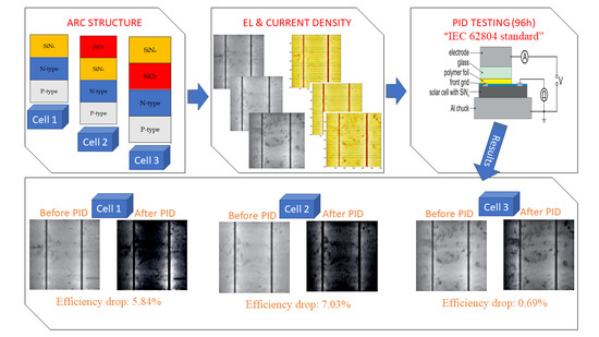
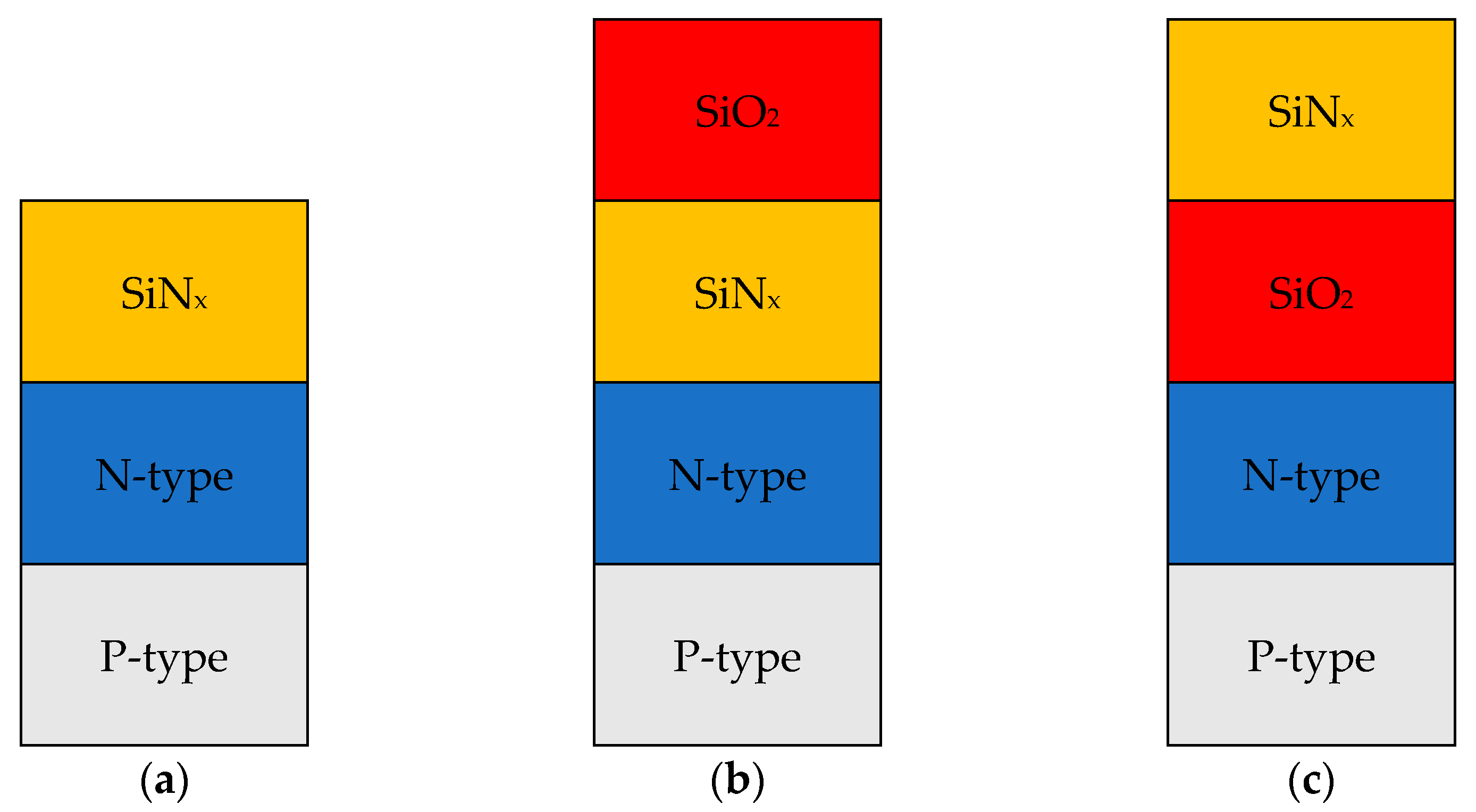
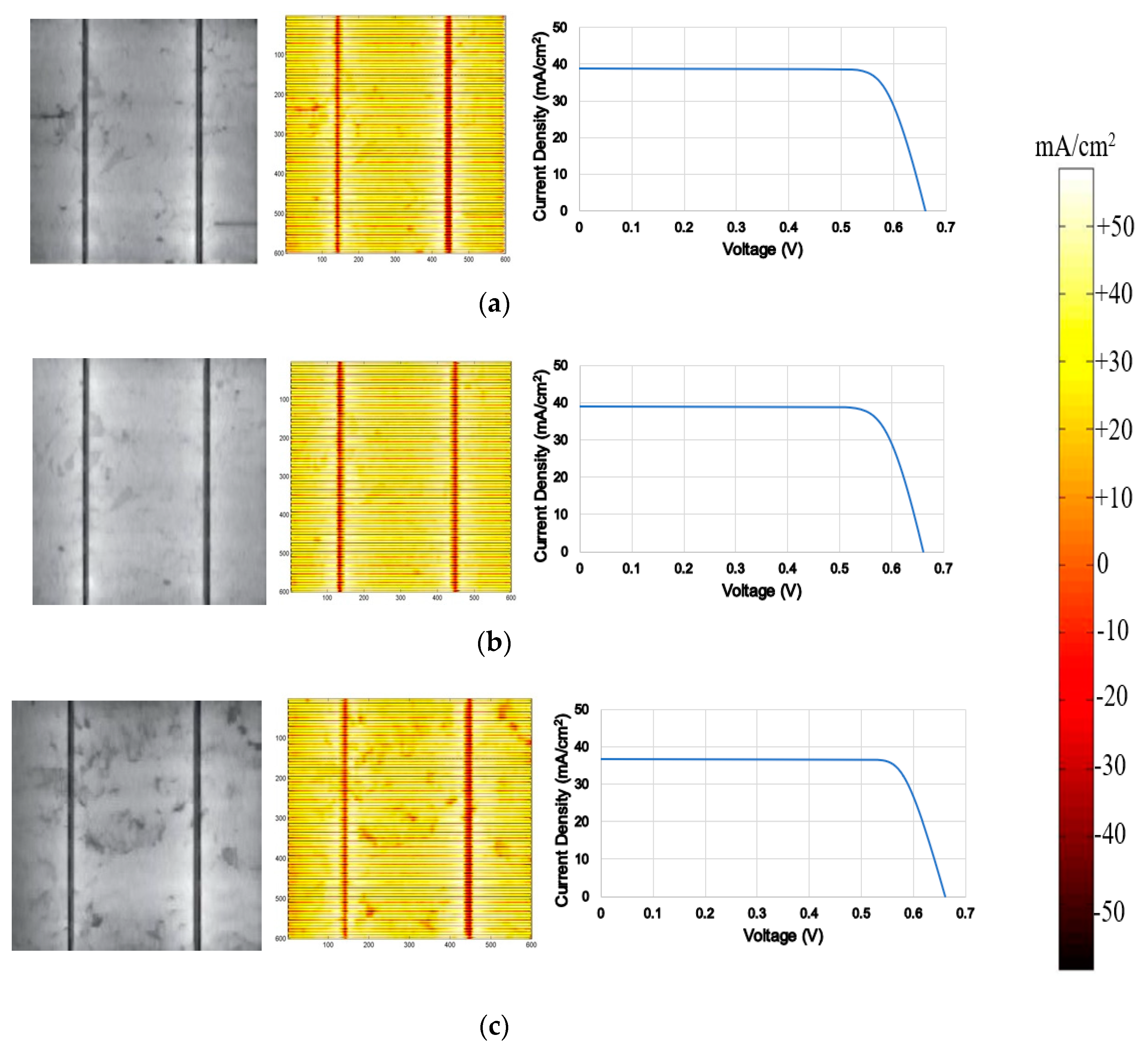
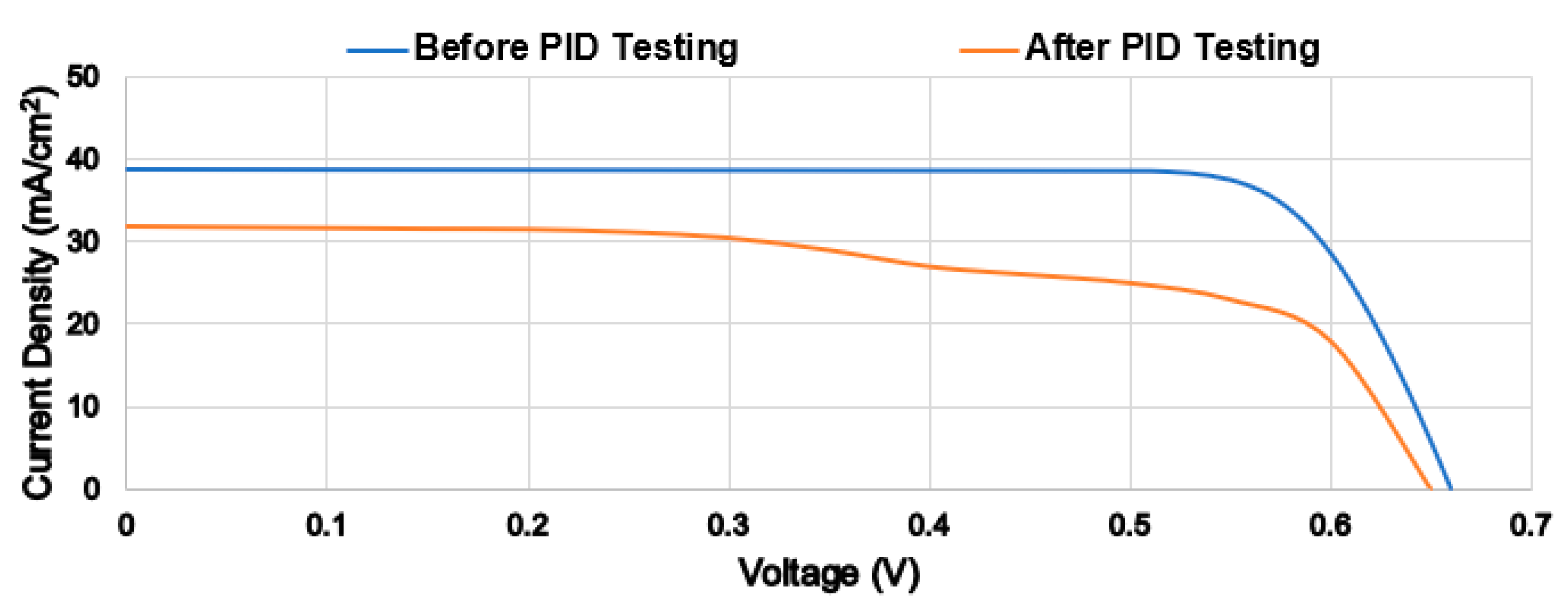
5.1. SiO2-Free (Cell #1)
5.2. SiO2 Thin Film Placed on the Top of the SiNx (Cell #2)
5.3. SiO2 Thin Film Placed on the Bottom of the SiNx (Cell #3)
- Enhance the stability of the solar cell structure, because there will be a limited leakage of the current at the top layer (SiNx), preventing mismatched conditions of the solar cell, particularly during the PID test [26].
- As there will be a limited leakage of the current, the expected drop in efficiency will also be at a minimum level. In addition, a drop in the shunt resistance is expected during PID testing [27]. However, it will be a limited drop as the current density will remain at its highest.
6. Conclusions
Author Contributions
Funding
Conflicts of Interest
References
- Siddig, M.H.; Hashim, S.M.; Osman, A.E. Formulation of an efficiency correlation for mono-crystalline PV modules using dimensional analysis. Sol. Energy 2020, 205, 456–460. [Google Scholar] [CrossRef]
- Wang, A.; Xuan, Y. A detailed study on loss processes in solar cells. Energy 2018, 144, 490–500. [Google Scholar] [CrossRef]
- Slauch, I.M.; Deceglie, M.G.; Silverman, T.J.; Ferry, V.E. Model for characterization and optimization of spectrally selective structures to reduce the operating temperature and improve the energy yield of photovoltaic modules. ACS Appl. Energy Mater. 2019, 2, 3614–3623. [Google Scholar] [CrossRef]
- Chen, T.C.; Kuo, T.W.; Lin, Y.L.; Ku, C.H.; Yang, Z.P.; Yu, I.S. Enhancement for potential-induced degradation resistance of crystalline silicon solar cells via anti-reflection coating by industrial PECVD methods. Coatings 2018, 8, 418. [Google Scholar] [CrossRef] [Green Version]
- Islam, M.A.; Hasanuzzaman, M.; Abd Rahim, N. A comparative investigation on in-situ and laboratory standard test of the potential induced degradation of crystalline silicon photovoltaic modules. Renew. Energy 2018, 127, 102–113. [Google Scholar] [CrossRef]
- Dhimish, M.; Holmes, V. Solar cells micro crack detection technique using state-of-the-art electroluminescence imaging. J. Sci. Adv. Mater. Dev. 2019, 4, 499–508. [Google Scholar] [CrossRef]
- Oh, J.; Bowden, S.; TamizhMani, G. Potential-induced degradation (PID): Incomplete recovery of shunt resistance and quantum efficiency losses. IEEE J. Photovolt. 2015, 5, 1540–1548. [Google Scholar] [CrossRef]
- Koentopp, M.B.; Kröber, M.; Taubitz, C. Toward a PID test standard: Understanding and modeling of laboratory tests and field progression. IEEE J. Photovolt. 2015, 6, 252–257. [Google Scholar] [CrossRef]
- Vieira, R.G.; de Araújo, F.M.; Dhimish, M.; Guerra, M.I. A Comprehensive Review on Bypass Diode Application on Photovoltaic Modules. Energies 2020, 13, 2472. [Google Scholar] [CrossRef]
- Dhimish, M.; Chen, Z. Novel Open-Circuit Photovoltaic Bypass Diode Fault Detection Algorithm. IEEE J. Photovolt. 2019, 9, 1819–1827. [Google Scholar] [CrossRef] [Green Version]
- Henry, C.; Poudel, S.; Lee, S.W.; Jeong, H. Automatic Detection System of Deteriorated PV Modules Using Drone with Thermal Camera. Appl. Sci. 2020, 10, 3802. [Google Scholar] [CrossRef]
- Hussain, M.; Dhimish, M.; Titarenko, S.; Mather, P. Artificial neural network based photovoltaic fault detection algorithm integrating two bi-directional input parameters. Renew. Energy 2020, 155, 1272–1292. [Google Scholar] [CrossRef]
- Dhimish, M. Thermal impact on the performance ratio of photovoltaic systems: A case study of 8000 photovoltaic installations. Case Stud. Therm. Eng. 2020, 21, 100693. [Google Scholar] [CrossRef]
- Devoto, I.; Halm, A. Comprehensive Study of PID Mechanisms for n-Type Bifacial Solar Cells. In Proceedings of the 36th European Photovoltaic Solar Energy Conference and Exhibition (EU PVSEC 2019), Marseille, France, 9–13 September 2019; pp. 1106–1113. [Google Scholar]
- Šlamberger, J.; Schwark, M.; Van Aken, B.B.; Virtič, P. Comparison of potential-induced degradation (PID) of n-type and p-type silicon solar cells. Energy 2018, 161, 266–276. [Google Scholar] [CrossRef]
- Masuda, A.; Hara, Y. Effect of light irradiation during potential-induced degradation tests for p-type crystalline Si photovoltaic modules. Jpn. J. Appl. Phys. 2018, 57, 08RG13. [Google Scholar] [CrossRef]
- Carolus, J.; Tsanakas, J.A.; van der Heide, A.; Voroshazi, E.; De Ceuninck, W.; Daenen, M. Physics of potential-induced degradation in bifacial p-PERC solar cells. Sol. Energy Mater. Sol. Cell. 2019, 200, 109950. [Google Scholar] [CrossRef] [Green Version]
- Wang, Q. Research on the effect of encapsulation material on anti-PID performance of 1500 V solar module. Optik 2020, 202, 163540. [Google Scholar] [CrossRef]
- López-Escalante, M.C.; Caballero, L.J.; Martín, F.; Gabás, M.; Cuevas, A.; Ramos-Barrado, J.R. Polyolefin as PID-resistant encapsulant material in PV modules. Sol. Energy Mater. Sol. Cell. 2016, 144, 691–699. [Google Scholar] [CrossRef]
- Jung, D.; Oh, K.S.; Jang, E.; Chan, S.I.; Ryu, S. Thickness Effect of SiO x Layer Inserted between Anti-Reflection Coating and pn Junction on Potential-Induced Degradation (PID) of PERC Solar Cells. J. Microelectron. Packag. Soc. 2019, 26, 75–80. [Google Scholar]
- Faur, O.; Faur, M. Mitigation of Potential-Induced Degradation. In Proceedings of the 2017 IEEE 44th Photovoltaic Specialist Conference (PVSC), Washington, DC, USA, 25–20 June 2017; pp. 896–899. [Google Scholar]
- Bora, B.; Oh, J.; Tatapudi, S.; Sastry, O.S.; Kumar, R.; Prasad, B.; Tamizhmani, G. Mitigation of PID in Commercial PV Modules Using Current Interruption Method. In Reliability of Photovoltaic Cells, Modules, Components, and Systems; SPIE: Bellingham, WA, USA, 2017; Volume 10370, p. 103700D. [Google Scholar]
- Boulhidja, S.; Mellit, A.; Voswinckel, S.; Lughi, V.; Ciocia, A.; Spertino, F.; Massi Pavan, A. Experimental Evidence of PID Effect on CIGS Photovoltaic Modules. Energies 2020, 13, 537. [Google Scholar] [CrossRef] [Green Version]
- Bonilla, R.S.; Al-Dhahir, I.; Yu, M.; Hamer, P.; Altermatt, P.P. Charge fluctuations at the Si–SiO2 interface and its effect on surface recombination in solar cells. Sol. Energy Mater. Sol. Cell. 2020, 215, 110649. [Google Scholar] [CrossRef]
- Dhimish, M.; Mather, P. Ultrafast High-Resolution Solar Cell Cracks Detection Process. IEEE Trans. Ind. Inf. 2020, 16, 4769–4777. [Google Scholar] [CrossRef] [Green Version]
- Yoo, G.Y.; Azmi, R.; Kim, C.; Kim, W.; Min, B.K.; Jang, S.Y.; Do, Y.R. Stable and colorful perovskite solar cells using a nonperiodic SiO2/TiO2 multi-nanolayer filter. ACS Nano 2019, 13, 10129–10139. [Google Scholar] [CrossRef] [PubMed]
- Dhimish, M.; Mather, P.; Holmes, V. Novel photovoltaic hot-spotting fault detection algorithm. IEEE Trans. Dev. Mater. Reliab. 2019, 19, 378–386. [Google Scholar] [CrossRef]


| Sample | Jsc (mA/cm2) | Voc (V) | FF (%) | Pmax (W) | Rsh (Ω) | Efficiency (%) |
|---|---|---|---|---|---|---|
| Cell #1 | 37.77 | 0.68 | 77.1 | 0.48 | 87.7 | 19.80 |
| Cell #2 | 38.91 | 0.68 | 76.8 | 0.49 | 84.4 | 20.32 |
| Cell #3 | 37.72 | 0.66 | 77.3 | 0.46 | 89.2 | 19.24 |
| Solar Cell #1 | Jsc (mA/cm2) | Voc (V) | FF (%) | Pmax (W) | Rsh (Ω) | Efficiency (%) |
|---|---|---|---|---|---|---|
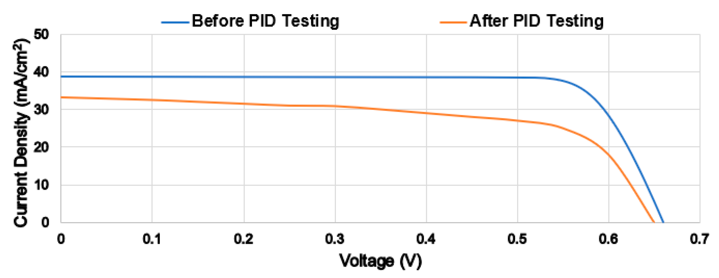
| Before PID | 37.77 | 0.68 | 77.1 | 0.48 | 87.7 | 19.80 |
| After PID | 33.2 | 0.66 | 63.7 | 0.37 | 9.12 | 13.96 |
| Solar Cell #1 | Jsc (mA/cm2) | Voc (V) | FF (%) | Pmax (W) | Rsh (Ω) | Efficiency (%) |
|---|---|---|---|---|---|---|
| Before PID | 38.91 | 0.68 | 76.8 | 0.49 | 84.4 | 20.32 |
| After PID | 31.90 | 0.66 | 63.1 | 0.35 | 7.51 | 13.29 |
| Solar Cell #1 | Jsc (mA/cm2) | Voc (V) | FF (%) | Pmax (W) | Rsh (Ω) | Efficiency (%) |
|---|---|---|---|---|---|---|
| Before PID | 37.72 | 0.66 | 77.3 | 0.46 | 89.2 | 19.24 |
| After PID | 36.88 | 0.66 | 76.2 | 0.45 | 85.7 | 18.55 |
| Solar Cell Parameter | Cell #1 | Cell #2 | Cell #3 |
|---|---|---|---|
| Jsc | 12.10% | 18.00% | 2.23% |
| Voc | 2.94% | 2.94% | 0% |
| FF | 13.40% | 13.70% | 1.1% |
| Pmax | 22.92% | 28.57% | 2.17% |
| Rsh | 89.60% | 91.10% | 3.92% |
| Efficiency | 5.84% | 7.03% | 0.69% |
© 2020 by the authors. Licensee MDPI, Basel, Switzerland. This article is an open access article distributed under the terms and conditions of the Creative Commons Attribution (CC BY) license (http://creativecommons.org/licenses/by/4.0/).
Share and Cite
Dhimish, M.; Hu, Y.; Schofield, N.; G. Vieira, R. Mitigating Potential-Induced Degradation (PID) Using SiO2 ARC Layer. Energies 2020, 13, 5139. https://doi.org/10.3390/en13195139
Dhimish M, Hu Y, Schofield N, G. Vieira R. Mitigating Potential-Induced Degradation (PID) Using SiO2 ARC Layer. Energies. 2020; 13(19):5139. https://doi.org/10.3390/en13195139
Chicago/Turabian StyleDhimish, Mahmoud, Yihua Hu, Nigel Schofield, and Romênia G. Vieira. 2020. "Mitigating Potential-Induced Degradation (PID) Using SiO2 ARC Layer" Energies 13, no. 19: 5139. https://doi.org/10.3390/en13195139