Abstract
A soft switching boost converter, with a small number of components and constant frequency control, is proposed herein by using the quasi-resonance method and the zero-voltage-transition method, realizing (1) the zero-voltage switching during the switch-on transient of the main switch, (2) the zero-current switching during the switch-off transient of the main switch, (3) the zero-current switching during the switch-on transient of the auxiliary switch, and (4) the zero-current switching during the switch-off transient of the auxiliary switch. Accordingly, the corresponding efficiency can be improved. The feasibility and effectiveness of the proposed structure are validated by the field programmable gate array (FPGA).
1. Introduction
As generally recognized, the switching power supply, which can operate at high frequency, has the advantages of small size, light weight, high efficiency, large voltage input range, etc. Switching power electronic converters can be roughly classified into the following three types: (a) traditional pulse-width modulation (PWM) power electronic converters; (b) resonant power electronic converters; (c) soft switching power electronic converter.
1.1. Traditional PWM Power Electronic Converter
As far as the traditional PWM power electronic converter is concerned, the PWM control technology is employed to control the on and off time of the power switch to realize the purpose of output voltage boosting or bucking. By increasing the switching frequency, the size of the inductor and capacitor can be reduced. In addition, when the power switch is operated in the on or off region, theoretically the power loss of the power switch is almost zero. However, due to the parasitic components in the circuit, when the power switch is switched, the voltage on the switch or the current in the switch is not zero momentarily, resulting in additional switching loss. This switching method is called hard switching. Therefore, in order to miniaturize the magnetic components and electrolytic capacitors, the switching frequency required for the converter should go up. However, when the switching frequency increases, the switching loss of the power switch during switch on and switch off will also increase. In addition to causing energy loss, it will also increase the heat sink required by the power switch, increasing the volume. Furthermore, when the switch is switched, the parasitic components of the circuit are prone to generate voltage surges or current surges or both, and this not only increases the stresses of the circuit components but also is a source of electromagnetic interference (EMI), which will interfere with the normal action of the control circuit.
1.2. Resonant Power Electronic Converter
Based on the foregoing, we can see that since the switching of the traditional PWM power electronic converter belongs to hard switching, serious switching losses are caused, and the efficiency cannot be improved. Resonant power electronic converters are the traditional PWM power electronic converters with inductor and switch connected in series or capacitor and switch connected in parallel to form a resonant circuit, so that the current or voltage on the power switch becomes a sine wave, reducing the overlap area of the current and voltage waveforms during the switching transient. Hence, reducing power loss leads to increasing the efficiency of the converter. This type of power electronic converter can be divided into: (1) traditional resonant converter (RC) [1,2,3]; (2) resonant-switch converter [4,5,6].
1.2.1. Traditional Resonant Converter (RC)
Traditional resonant converters are also called load-resonant converters. This converter includes an inductance-capacitance (LC) resonant tank. The resonant tank is in series or parallel with the load terminal, and the resonant components participate in the whole process of converter energy conversion. Using the resonant voltage or current generated by the resonance tank achieves zero-voltage switching (ZVS) or zero-current switching (ZCS). The power required by the load can be adjusted by the resonant tank circuit.
1.2.2. Resonant-Switch Converter
Resonant-switch power electronic converters only utilize resonant components to create resonance when the switch is switched to provide the voltage or current required for zero switching of the switch. The resonant energy only partially participates in the energy conversion process of the converter. Such a converter is called a quasi-resonant converter (QRC) and can be divided into zero-current-switching quasi-resonant converter (ZCS-QRC) and zero-voltage-switching quasi-resonant converter (ZVS-QRC).
1.3. Soft Switching Power Electronic Converter
The soft switching power converter uses auxiliary switches and resonant components to act, so that the main power switch resonates only at the moment of switching. Because resonance only occurs the moment the main power switch is switched, no resonance occurs during the rest of the time and hence constant frequency control can be realized. Soft switching power electronic converters can be classified into the following three types: (1) ZCS/ZVS PWM power converter; (2) zero-voltage transition (ZVT)/zero-current transition (ZCT) power converter; (3) ZCZVT power converter. Their characteristics are as follows.
1.3.1. ZCS/ZVS PWM Power Converter
Adding an auxiliary switch to the quasi-resonant circuit and using the auxiliary switch to control when the resonance works make the resonance pause for a period of time adjustable, and this improves the shortcomings of fixed on or off time of quasi-resonant power converters [7,8,9,10]. That is, the resonance time can be controlled by the auxiliary switch without changing the switching frequency so that constant frequency control can be realized. However, the components should endure high voltage or current stress due to resonance, thereby causing serious conduction loss.
1.3.2. ZVT/ZCT Power Converter
Placing the resonance element on the non-main energy transmission path reduces conduction loss [11,12,13]. Prior to the main switch being switched on, the auxiliary switch is switched on to form a resonant circuit, which generates transient resonance, so that the voltage on or current in the main switch resonates to zero and then this switch is switched. When the auxiliary switch is not switched, the converter does not resonate and will not cause high voltage or high current stress. Therefore, the conduction loss can be reduced. In addition, constant frequency control can be used, and hence the filter design is easy. However, ZVT converter can only achieve zero-voltage switching, whereas ZCT converter can only achieve zero-current switching.
1.3.3. ZCZVT Power Converter
As the main switch is switched to the pre-transient state of the switch on and the post-transient state of the switch off, respectively, the auxiliary switch will be turned on first to form a resonant circuit, so that the voltage on and current in the main switch resonate to zero, achieving zero-voltage switching and zero-current switching [14,15,16,17]. Therefore, the main switch has both functions of ZVT and ZCT. Over one switching cycle, a total of two transient resonances occurs, and these two transient resonances only occupy a small proportion of the entire switching cycle. As the auxiliary switch does not operate, the ZCZVT power converter acts like a traditional PWM power electronic converter. That is, this soft switching method can reduce component stress and conduction loss, and such a converter can be controlled by a constant frequency. Although this converter can reach ZVT and ZCT, the auxiliary switch over one switching cycle should produce two transient resonances, so the circuit design is complicated and there are many components, resulting in cost increase.
In order to realize the zero-voltage or zero-current switching of the main switch, the above-mentioned individual structures can be adopted, depending on the situation. However, the general soft switching power electronic converter requires additional complex auxiliary circuits, which increases the number of components [7]. Moreover, most of the auxiliary switches of soft switching power electronic converters are floating, and this increases the complexity of the circuit design [14]. In summary, although the general soft switching power electronic converter can increase the switching frequency, reduce electromagnetic interference (EMI), and reduce the component stress of the switch, the addition of too many components can tend to lead to higher cost, larger volume and inability to effectively improve efficiency.
Based on the mention above, this paper presents a soft switching boost converter, with a small number of components and constant frequency control by using the QR method and the ZVT method, to achieve the zero-voltage switching during the switch-on transient of the main switch and the zero-current switching during the switch-off transient of the main switch as well as to achieve the zero-current switching during the switch-on transient of the auxiliary switch and the zero-current switching during the switch-off transient of the auxiliary switch.
2. Proposed Circuit
Figure 1 displays the proposed soft switching boost converter, which is constructed by one traditional boost converter along with one auxiliary switch module. The former is constructed by one input inductor Lin, one main switch S1 along with one body diode D1, one output diode Do, and one output capacitor Co. The latter is established by one auxiliary switch S2 along with one body diode D2, one resonant diode Dr, one resonant inductor Lr, one resonant capacitor Cr. The output load is represented by one resistor RL.
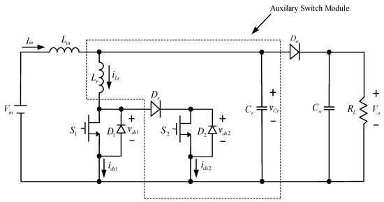
Figure 1.
Proposed soft switching boost converter.
3. Basic Operating Principles
The behavior of the proposed converter with soft switching will be described as follows. Prior to this, the symbols and assumptions relevant to this circuit shown in Figure 1 will be given: (i) Vin is the DC input voltage; (ii) iLr is the current flowing through Lr; (iii) vCr is the voltage imposed on Cr; and (iv) all the components are ideal except that the switches have individual body diodes. There are nine states in the converter operating, as shown in Figure 2. In the following description, ωr and Zr are called resonant radian frequency and characteristic impedance, respectively, and are equal to
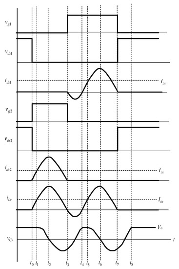
Figure 2.
Illustrated waveforms relevant to the proposed soft switching boost converter operating.
3.1. State 0
As displayed in Figure 2 () and Figure 3a, both of S1 and S2 are in the off state. Before S2 is switched on, the current Iin will flow through Do. In this time interval, the voltage imposed on Cr is the voltage Vo. Once S2 is switched on, the operation proceeds to state 1. Two state equations for state 0 is
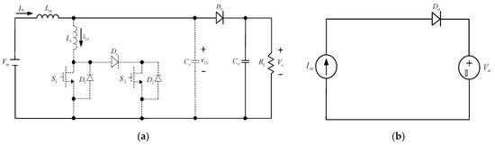
Figure 3.
(a) Current flow in state 0; (b) Equivalent circuit of (a).
3.2. State 1
As displayed in Figure 2 and Figure 4a, S1 is still in the off state, but S2 is switched on with the current going up from zero and Dr conducted. Hence, S2 has ZCS switch on. During the initial switch-on transient of S2, the diode Do is still in the on state, the current iLr is linearly increased. Before iLr increases to the current Iin, the voltage vCr is kept constant at Vo. As soon as iLr increases to Iin, the diode Do is turned off, proceeding to state 2. The time elapsed is derived below.
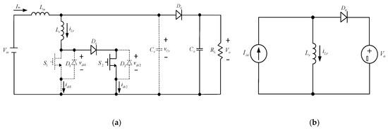
Figure 4.
(a) Current flow in state 1; (b) Equivalent circuit of (a).
The initial values of this state are
Based on Figure 4b, one state equation can be obtained to be
Substituting (3) into (4) yields
Since iLr(t1) = Iin, we can obtain the corresponding time elapsed from (5) as
3.3. State 2
As displayed in Figure 2 and Figure 5a, S1 is still in the off state but S2 is still in the on state. Since S2 keeps conducting, Lr keeps resonating with Cr. In this time interval, the energy stored in Cr is passed to Lr, thereby making vCr decreased. The moment vCr decreases to zero, the operation goes to state 3. The time elapsed is derived below.
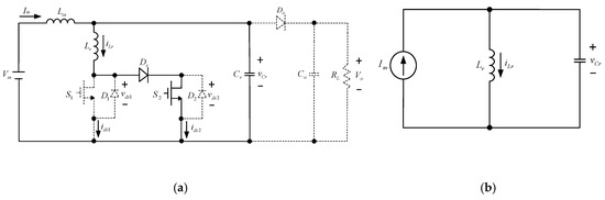
Figure 5.
(a) Current flow in state 2; (b) Equivalent circuit of (a).
The initial values of this state are
Based on Figure 5b, two state equations can be obtained to be
By applying the Laplace transform to (8), we can obtain
Therefore, we can obtain the solution of (9) as
By applying the inverse Laplace transform to (10), we can obtain
Substituting (7) into (11) yields
Since , we can obtain the corresponding time elapsed from (12) as
3.4. State 3
As displayed in Figure 2 and Figure 6a, S1 is still in the off state, but S2 is still in the on state. In this time interval, Lr still resonates with Cr. Once iLr drops to zero, S1 is switched on but S2 is switched off with ZCS, the operation proceeds to state 4. The time elapsed is derived below.
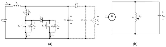
Figure 6.
(a) Current flow in state 3; (b) Equivalent circuit of (a).
The initial values of this state are
Based on Figure 6b, two state equations can be obtained to be
By applying the Laplace transform to (15), we can obtain
Therefore, we can obtain the solution of (16) as
By applying the inverse Laplace transform to (17), we can obtain
Substituting (14) into (18) yields
Since , we can obtain the corresponding time elapsed from (19) as
3.5. State 4
As displayed in Figure 2 and Figure 7a, S1 is switched on, but S2 is switched off. Since the voltage on S1 is clamped at zero in state 3, S1 is switched on with ZVS. In this time interval, iLr is negative with a peak value of Iin − Vo/Zr. Once iLr is zero again, the operation moves to state 5. The time elapsed is derived below.
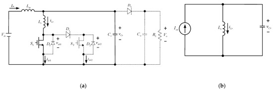
Figure 7.
(a) Current flow in state 4; (b) Equivalent circuit of (b).
The initial values of this state are
Based on Figure 7b, two state equations can be obtained to be
By applying the Laplace transform to (22), we can obtain
Therefore, we can obtain the solution of (23) as
By applying the inverse Laplace transform to (24), we can obtain
Substituting (21) into (25) yields
Since and , we can obtain
Therefore, we can obtain the corresponding time elapsed from (27) as
3.6. State 5
As displayed in Figure 2 and Figure 8a, S1 is still in the on state, but S2 is still in the off state. In this time interval, vCr resonates to Vo and then keeps constant at Vo. The current Iin flows into Lr, causing iLr to be linearly increased. As soon as iLr rises to Iin, the operation moves to state 6. The time elapsed is derived below.
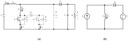
Figure 8.
(a) Current flow in state 5; (b) Equivalent circuit of (a).
The initial values of this state are
Based on Figure 8b, one state equation can be obtained to be
Substituting (29) into (30) yields
Since , we can obtain the corresponding time elapsed from (31) as
3.7. State 6
As displayed in Figure 2 and Figure 9a, S1 is still in the on state, but S2 is still in the off state. In this time interval, Cr resonates with Lr. The capacitor Cr transfers energy to Lr. That is, vCr begins to fall and iLr resonantly rises. Once vCr decreases to zero, the operation goes to state 7. The time elapsed is derived below.
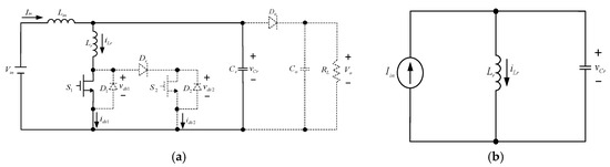
Figure 9.
(a) Current flow in state 6; (b) Equivalent circuit of (a).
The initial values of this state are
Based on Figure 9b, two state equations can be obtained to be
By applying the Laplace transform to (34), we can obtain
Therefore, we can obtain the solution of (35) as
By applying the inverse Laplace transform to (36), we can obtain
Substituting (33) to (37) yields
Since , we can obtain the corresponding time elapsed from (38) as
3.8. State 7
As displayed in Figure 2 and Figure 10a, S1 is still in the on state, but S2 is still in the off state. In this time interval, Lr still resonates with Cr. As iLr drops to zero, S1 is switched off with ZCS. Once S1 is switched off, the operation proceeds to state 8. The time elapsed is derived below.
Figure 10.
(a) Current flow in state 7; (b) Equivalent circuit of (a).
The initial values of this state are
Based on Figure 10b, two state equations can be obtained to be
By applying the Laplace transform to (41), we can obtain
Therefore, we can obtain the solution of (42) as
By applying the inverse Laplace transform to (43), we can obtain
Substituting (40) to (44) yields
Since , we can obtain the corresponding time elapsed from (45) as
3.9. State 8
As displayed in Figure 2 and Figure 11a, S1 is switched off, and S2 is still in the off state. During this state, the resonant behavior stops. iLr is kept constant at zero. Cr is charged by Iin, thereby making vCr increased. The moment vCr increases to Vo, the diode Do is conducted, and the operation moves to state 0 with the next cycle repeated. The time elapsed is derived below.
Figure 11.
(a) Current flow in state 8; (b) Equivalent circuit of (b).
The initial values of this state are
Based on Figure 11b, one state equation can be obtained to be
Substituting (47) to (48) yields
Since , we can obtain the corresponding time elapsed from (49) as
4. Design Considerations
Table 1 shows the system specifications. Based on Table 1, and Section 2, the input inductor Lin, the output capacitor Co, the resonant capacitor Cr, and the resonant Lr will be figured out.

Table 1.
System and specifications (CCM: continuous conduction mode).
4.1. Design for Lin
As this converter works in the continuous conduction mode (CCM) above Io,min, the following equation is used to find the minimum input inductor Lin,min [12], based on Table 1:
Eventually, Lin is selected as 100 μH so as to make sure that such a converter works in CCM.
4.2. Design for Co
By assuming that the output ripple voltage is lower than 0.1%, the following equation is used to find the minimum output capacitor Co,min, based on Table 1:
Finally, Co is selected as 220 μF.
4.3. Design for Lr
By assuming that there are two resonant cycles per one half of the PWM period and no resonant cycles per the other half of the PWM period, and the time elapsed for state 1 is the fifth of the resonant period, the value of Lr can be worked out as follows:
Finally, Lr is selected as 2 μH.
4.4. Design for Cr
In state 2, vCr(t1) = Vo and iLr(t1) = Iin. In order to make sure that the resonant behavior will happen, the following inequality should be obeyed:
Finally, Cr is selected as 22 nF.
5. Experimental Results
At rated load, Figure 12 displays the PWM signals vg1 and vg2 for S1 and S2; Figure 13 displays the PWM signal vg1 for S1, the voltage on S1, named vds1, and the current in S1, named ids1; Figure 14 shows the PWM signal vg2 for S2, the voltage on S2, named vds2, and the current in S2, named ids2; Figure 15 displays iLr and vCr. In Figure 12, we can see that the switch-on instant for S2 is prior to that for S1. In Figure 13, we can see that S1 has ZVT switch on and ZCS switch off. In Figure 14, we can see that S2 has ZCS switch on and ZCS switch off. In Figure 15, we can see that VCr and iLr have two resonant cycles per one half of PWM cycle and no resonant cycles per the other half of PWM cycle.
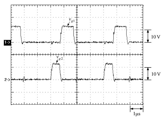
Figure 12.
PWM signals for S1 and S2: (1) vg1; (2) vg2.
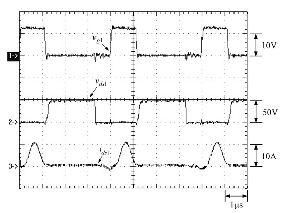
Figure 13.
Waveforms relevant to S1: (1) vg1; (2) vds1; (3) ids1.
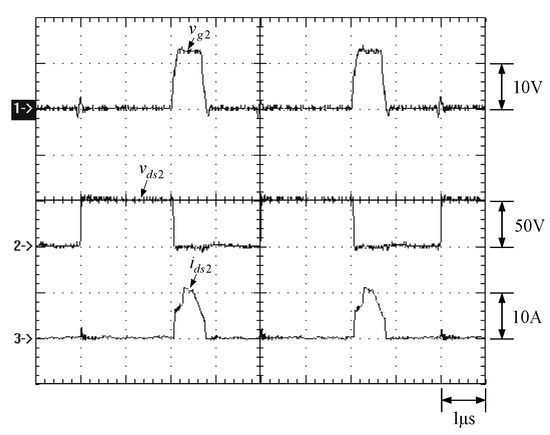
Figure 14.
Waveforms relevant to S2: (1) vg2; (2) vds2; (3) ids2.
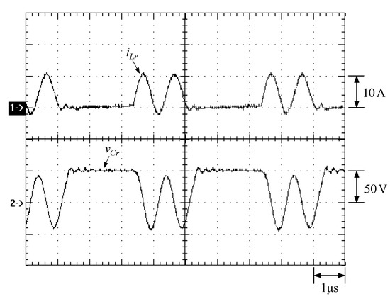
Figure 15.
Resonant current iLr and resonant voltage vCr.
Moreover, Figure 16 displays how to measure the efficiency. First of all, the input current Iin is obtained by using one digital meter called Fluke 8050 A to measure the voltage across the current sensor. Afterwards, the input voltage Vin is attained by another digital meter. Hence, the input power is equal to the product of Vin and Iin. As for the output power, the output current Io is obtained from the electronic load and the output voltage Vo is attained by the other digital meter. Therefore, the output power is equal to the product of Vo and Io. Finally, the resulting efficiency can be attained. Figure 17 shows the relationship between efficiency and load. In Figure 17, we can see that the maximum difference in efficiency between soft switching and hard switching is about 2%. Figure 18 shows a photo of the experimental setup.
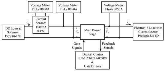
Figure 16.
Efficiency measurement.
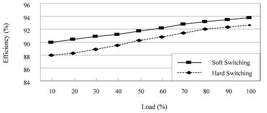
Figure 17.
Efficiency comparison.
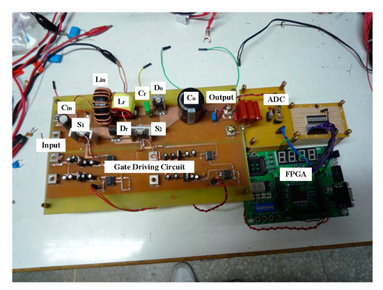
Figure 18.
Photo of the experimental setup.
6. Comparisons
The circuit shown in [13] is chosen as a comparison. In Table 2, the number of resonant components for the circuit shown in [13] is six, whereas the number of resonant components for the proposed circuit is four. The circuit shown in [13] has the ZVT turn on for the main switch, whereas the proposed circuit has the ZVT turn on and ZCS turn on for the main switch. The maximum value of the overall efficiency for the circuit shown in [13] is 96.2% with switching frequency of 30 kHz, whereas that for the proposed circuit is 93.8% with switching frequency of 250 kHz. It is noted that the lower the switching frequency, the higher the efficiency.
Table 2.
Comparisons between [13] and the proposed circuits (ZVT: zero-voltage transition; ZCS: zero-current transition).
7. Conclusions
In this paper, by combining QR and ZVT, an auxiliary circuit, with a small number of components containing Lr, Cr and S1, is added to the traditional boost converter, so as to realize the ZVT switch on and ZCS switch off of S1 as well as the ZCS switch on and ZCS switch off of S2. Accordingly, the difference in efficiency at light load between soft switching and hard switching is about 2%. In addition to improving the shortcomings of general resonant power electronic converters that require variable frequency control, this structure has the advantage of constant frequency control.
Author Contributions
Conceptualization, Y.-T.Y.; methodology, K.-I.H.; software, J.-J.S.; validation, Y.-T.Y.; formal analysis, Y.-T.Y.; investigation, J.-J.S.; resources, K.-I.H.; data curation, J.-J.S.; writing—original draft preparation, K.-I.H.; writing—review and editing, K.-I.H.; visualization, J.-J.S.; supervision, K.-I.H.; project administration, Y.-T.Y.; funding acquisition, J.-J.S. All authors have read and agreed to the published version of the manuscript.
Funding
This research was funded by the Ministry of Science and Technology, Taiwan, under the Grant Number: MOST 109-2622-E-035-009-CC3.
Conflicts of Interest
The authors declare no conflict of interest.
References
- Ye, Z.M.; Jain, P.K.; Sen, P.C. Two stage resonant inverter for AC distributed power supply. IEEE IECON 2004, 1, 239–244. [Google Scholar]
- Li, J.; Niu, Z.; Zhou, D.; Shi, Y. Analysis of series-parallel resonant converter with multipliers. In Proceedings of the 2005 IEEE International Symposium on Circuits and Systems (IEEE ISCAS’05), Kobe, Japan, 23–26 May 2005; Volume 5, pp. 4449–4452. [Google Scholar]
- Chen, H.; Sng, E.K.K.; Tseng, K.J. Generalized optimal trajectory control for closed loop control of series-parallel resonant converter. IEEE Trans. Power Electron. 2006, 21, 1347–1355. [Google Scholar] [CrossRef]
- Lee, F.C. High-frequency quasi-resonant converter technologies. Proc. IEEE 1988, 76, 377–390. [Google Scholar] [CrossRef]
- Chuang, Y.-C.; Ke, Y.-L. A novel high-efficiency battery charger with a buck zero-voltage-switching resonant converter. IEEE Trans. Energy Convers. 2007, 22, 848–854. [Google Scholar] [CrossRef]
- Jiang, Y.; Yang, Y.; Cheng, R. Research on the passive integration in ZCS buck quasi-resonant converter. In Proceedings of the 2005 International Conference on Electrical Machines and Systems (IEEE ICEMS’05), Nanjing, China, 27–29 September 2005; Volume 2, pp. 1136–1340. [Google Scholar]
- Park, S.-R.; Park, S.-H.; Won, C.-Y.; June, Y.-C. Low loss soft switching boost converter. In Proceedings of the 2008 13th International Power Electronics and Motion Control Conference (IEEE EPE-PEMC’08), Poznan, Poland, 1–3 September 2008; pp. 181–186. [Google Scholar]
- Shi, L.; Chen, L.; Yin, C. A novel PWM soft switching DC-DC converter. In Proceedings of the INTELEC 06—Twenty-Eighth International Telecommunications Energy Conference (IEEE INTELEC’06), Providence, RI, USA, 10–14 September 2006; pp. 1–6. [Google Scholar]
- Claassens, J.; Hofsajer, I.W.; de Jager, K. Passive component integration in a ZVS flyback converter. In Proceedings of the Twenty-First Annual IEEE Applied Power Electronics Conference and Exposition (IEEE APEC’06), Dallas, TX, USA, 19–23 March 2006; Volume 6, pp. 539–544. [Google Scholar]
- Lo, Y.-K.; Lin, J.-Y. Active-clamping ZVS flyback converter employing two transformers. IEEE Trans. Power Electron. 2007, 22, 2416–2423. [Google Scholar] [CrossRef]
- Chang, B.; Wang, C.; He, Y. Research on switching boost converter. In Proceedings of the IEEE International Conference on Digital Manufacturing & Automation, Zhangjiajie, China, 5–7 August 2011; pp. 1015–1018. [Google Scholar]
- Yau, Y.-T.; Hwu, K.-I.; Jiang, W.-Z. Two-phase interleaved boost converter with ZVT turn-on for main switches and ZCS turn-off for auxiliary switches based on one resonant loop. Appl. Sci. 2020, 10, 3881. [Google Scholar] [CrossRef]
- Park, S.-H.; Part, S.-R.; Yu, J.-S.; Won, C.-Y. Analysis and design of soft-switching boost converter with an HI-bridge auxiliary resonant circuit. IEEE Trans. Power Electron. 2010, 25, 2142–2149. [Google Scholar] [CrossRef]
- Yang, S.P.; Lin, J.; Chen, S.J. A novel ZCZVT forward converter with synchronous rectification. IEEE Trans. Power Electron. 2006, 21, 912–922. [Google Scholar] [CrossRef]
- Lin, J.L.; Hsieh, J.C. Dynamics and control of ZCZVT boost converters. IEEE Trans. Power Electron. 2005, 52, 1919–1927. [Google Scholar]
- Lin, J.; Hsieh, J.C.; Yeh, I.C. A novel ZCZVT soft-switching signal-stage high power factor correction on converter. In Proceedings of the 2004 IEEE Asia-Pacific Conference on Circuits and Systems (IEEE APCCAS’04), Tainan, Taiwan, 6–9 December 2004; Volume 2, pp. 657–660. [Google Scholar]
- Hwu, K.-I.; Shieh, J.-J.; Jiang, W.-Z. Interleaved boost converter with ZVT-ZCT for main switches and ZCS for auxiliary switch. Appl. Sci. 2020, 10, 2033. [Google Scholar] [CrossRef]


Publisher’s Note: MDPI stays neutral with regard to jurisdictional claims in published maps and institutional affiliations. |
© 2020 by the authors. Licensee MDPI, Basel, Switzerland. This article is an open access article distributed under the terms and conditions of the Creative Commons Attribution (CC BY) license (http://creativecommons.org/licenses/by/4.0/).