Article

Thermo-Mechanical Stress Comparison of a GaN and SiC MOSFET for Photovoltaic Applications

1
Institute for Materials Research (IMO), Hasselt University, Wetenschapspark 1, 3590 Diepenbeek, Belgium
2
IMOMEC, IMEC, Wetenschapspark 1, 3590 Diepenbeek, Belgium
3
EnergyVille, Thorpark 8320, 3600 Genk, Belgium
*
Author to whom correspondence should be addressed.
Energies 2020, 13(22), 5900; https://doi.org/10.3390/en13225900
Submission received: 10 October 2020 / Revised: 9 November 2020 / Accepted: 10 November 2020 / Published: 12 November 2020
(This article belongs to the Section A2: Solar Energy and Photovoltaic Systems)

Abstract

:
Integrating photovoltaic applications within urban environments creates the need for more compact and efficient power electronics that can guarantee long lifetimes. The upcoming wide-bandgap semiconductor devices show great promise in providing the first two properties, but their packaging requires further testing in order to optimize their reliability. This paper demonstrates one iteration of the design for reliability methodology used in order to compare the generated thermo-mechanical stress in the die attach and the bond wires of a GaN and SiC MOSFET. An electro-thermal model of a photovoltaic string inverter is used in order to translate a cloudy and a clear one-hour mission profile from Arizona into a junction losses profile. Subsequently, the finite element method models of both devices are constructed through reverse engineering in order to analyze the plastic energy. The results show that the plastic energy in the die attach caused by a cloudy mission-profile is much higher than that caused by a clear mission-profile. The GaN MOSFET, in spite of its reduced losses, endures around 5 times more plastic energy dissipation density in its die attach than the SiC MOSFET while the reverse is true for the bond wires. Potential design adaptations for both devices have been suggested to initiate a new iteration in the design for reliability methodology, which will ultimately lead to a more reliable design.

1. Introduction

Population growth and the excessive use of electrical appliances have an enormous influence on the electricity consumption, which mainly comes from fossil fuels. Over the past decades, alternative sources of energy have received special attention in many countries, mainly because of greenhouse gas emissions, global warming, and ozone layer depletion. In order to stabilize the Earth’s climate, a long-term plan must be put in place in order to replace most of the present energy systems with net-zero emission energy systems over the next few decades [1]. In this regard, the share of renewable energies should increase significantly. Solar energy is one of the key investments to tackle the aforesaid issues; and, based on a study that was conducted by the European Photovoltaic Industry Association (EPIA), photovoltaic (PV) technologies have enormous potential over the years ahead [2]. The photovoltaic industry can be supported by governments by the fulfillment of the suitable financial conditions as the electricity produced by solar panels would be cheaper than the fossil fuel generators in sunny regions [3].
Nowadays, there is great potential for integrating PV panels within urban environments and buildings. The typical PV panel system design involves installing PV panels on the rooftop of the building and according to the optimal tilt angle, so that the received solar irradiation can be maximized [4]. A relatively new application of photovoltaic systems is that the PV panel simultaneously plays a role as an integral part of the building design and a part of the solar power generation system [5]. This promising approach to generate electricity—which is known as building-integrated photovoltaics (BIPV)—offers several advantages, such as [5,6,7,8]:
  • Less space will be needed for the installation of PV panels.
  • Less installation and repair costs are required.
  • Lower distribution and transmission losses, because the electricity generated by the BIPV system will be consumed locally.
  • Lower heat transfer coefficients between different building partitions, which improves the building energy efficiency.
Therefore, traditional building elements can be substituted by BIPV systems, such as façades and windows [9]. In order to efficiently implement the PV technologies, a power electronic converter is required in order to act as the interface between the PV panel and the distribution network (or load). The improvement and expansion of electronic power systems in PV applications can be attributed to the remarkable development of power semiconductor devices and control systems [10]. In the residential sector, designs with modular inverters are a common solution for the interconnection between the PV panels and the grid/load in which each PV panel can be connected to an inverter constructing a standalone module [11]. In the BIPV systems, inverters are getting increasingly compact and adaptive, which makes growth markets more eager to jump on plug-and-play systems. Because the development of plug-and-play systems can lead to a flexibility and scalability in the entire system, it allows for more opportunities and choices for both consumers and installers to have a more efficient BIPV system [12].
Although many studies have conducted investigations on the BIPV applications and their challenges, there is a lack of study on the reliability issues of power electronic devices as an integral part within these systems. In power electronics systems, there are various components that are prone to failure—such as semiconductors, capacitors, controllers, and sensors—so that a failure in any of these components will cause downtime to the entire system [13]. The key to reliability is to be able to identify the most failure-prone components. According to the literature, electrolytic capacitors and switching devices are the most vulnerable components in the inverters [14]. Because the use of large capacitors can be avoided by modifying the circuit topology, the reliability problem can be partially solved to some extent [15]. According to [14], the switching devices have contributed enormously to the overall failure (approximately 85%). Thus, evaluating the reliability and estimating the lifetime accurately for these devices will have a significant impact on the system design. Although the silicon (Si) diode and the metal-oxide-semiconductor field-effect transistors (MOSFETs) now seem to be fairly common in the power converters used within PV applications, these devices are not compatible with the new PV conversion system requirements, including lower cost, higher switching frequency, higher blocking voltages, higher operating temperature, higher efficiency, and higher power density [16]. One of the proposed methods in this field is the replacement of silicon as the fabrication material with a wider bandgap material with certain carrier mobility [17]. Because of the great physical properties of these wide-bandgap (WBG) materials, two well-known materials—gallium nitride (GaN) and silicon carbide (SiC)—could promise a revolution in power electronics [18]. Because the intrinsic carrier concentration for these WBG materials is much lower than that of silicon, the breakdown voltage capability would be much higher even with thinner and highly doped layers, which makes operating at higher temperatures feasible for the semiconductor device [19].
Although there are benefits for these WBG materials over silicon, thin active layers and a smaller chip size have led to some additional mechanical stress in these devices, so that the temperature fluctuations and thermal mismatches have a greater impact on the mechanical stress of the layers [20]. The power semiconductor devices in power converters will behave differently, depending on the operating and environmental conditions and they may undergo sudden changes in their working condition [21]. This mission profile variation is known as a primary factor influencing the reliability of the power devices and has to be considered in the reliability assessments [22]. However, despite all of these challenges, because the compactness is at the top of the priority list for the PV applications (especially for BIPV systems), the wide-bandgap devices that are based on GaN and SiC are at the center of attention. Hence, there would be some drawbacks while working with these WBG devices that need to be highlighted (e.g., the bond wire and die attach would be more fragile because of the higher operating frequency).
Because to the limited information provided by the manufacturers about the internal packaging structure, a reverse engineering approach combined with finite element modeling is mandatory in order to gain further insights into the thermal stress that is caused within the different material layers. Together with the necessary experimental validation, the weak points in the packaging of both devices can be identified and further material improvements considering the design for reliability can be performed [23].
This paper consists of six sections in which one iteration of the design for reliability methodology is gradually applied on two commercially available GaN and SiC MOSFETs. Firstly, in Section 2, an electro-thermal model of a wide-bandgap based string inverter used in photovoltaic applications is constructed. This model is used to translate a photovoltaic mission profile into a MOSFET junction losses profile which will become the primary heat source in the subsequent finite element method (FEM) simulations. Additionally, the junction losses model used for these two MOSFETs is also validated through experimental testing. In Section 3, the reverse engineering of the GaN and SiC MOSFET is performed while using X-ray imaging, scanning electron microscopy (SEM), and energy-dispersive X-ray spectroscopy (EDX) in order to extract the shapes, dimensions, and materials of the various internal component elements. In Section 4, 3-D finite element models of both the MOSFETs are constructed while using the inputs that were obtained from the previous section. Furthermore, the simulated MOSFET case temperatures that are generated by the junction losses are validated through experimental testing. In Section 5, both of the FEM models are stressed by two different one-hour mission profiles and the regions with the highest plastic energy dissipation density are analyzed. Lastly, Section 6 draws the conclusion.

2. Electro-Thermal Modeling of a Wide-Bandgap Based String Inverter

To understand and quantify the thermo-mechanical stress that is generated in a semiconductor device that is used in a photovoltaic power converter, an electro-thermal model of the topology is required in order to translate the solar mission profile into a local power losses and/or temperature profile. In this paper, a traditional full-bridge string inverter is modelled while using either a GaN MOSFET or a SiC MOSFET. The temperature dependence of both the conduction losses and switching losses is included in the model as well as the maximum power point tracking (MPPT) algorithm. The heat transfer is modelled through a one-dimensional (1-D) lumped thermal network. The model is constructed while using PLECS Blockset (4.3, Plexim, Zurich, Switzerland) and Simulink (9.3, Mathworks, Natick, MA, USA).

2.1. Electro-Thermal Model Construction

The full-bridge string inverter topology, together with the chosen components, can be seen in Figure 1a. It converts 1430 W on the input at 1000 W/m2 irradiance and a maximum power point voltage of 385 V. A traditional LCL filter is employed at the output to filter the output harmonics. The chosen MMPT algorithm is based on the perturb & observe (P&O) method due to its simplicity and low cost. Additionally, a switching frequency of 100 kHz as well as a grid frequency of 50 Hz is used. The main heat generating source in this topology consists of the switching losses and the conduction losses of the MOSFET. Both can be calculated by using the datasheets provided by the manufacturer [24]. Modeling the temperature dependence of these losses is mandatory for reliability analyses according to a previously performed sensitivity analysis [25]. Other temperature dependences in the topology have a negligible impact on the thermo-mechanical degradation of the MOSFET. The 1-D steady-state Foster thermal network that was utilized to model the heat transfer is shown in Figure 1b, which also identifies the various conductive and convective thermal resistances. It only includes the losses of the switching devices, as they are generating the majority of the heat in this topology and are the main focus of this paper. Additional RA-T2X-25E heat sinks have been added in order to keep the junction temperatures of these devices within the operating limits at the maximum input power. The thermal resistances can either be extracted from the datasheets or calculated while using the cross-sectional surface and the thermal conductivity of the materials, as previously demonstrated in [25]. The heat is generated in the die and conducted through the case and heat sink towards either the surrounding air or the PCB. Lastly, the PCB transfers the heat to the surrounding air through a final convective thermal resistance. The extracted and calculated values of the thermal resistances can be found in Table 1.
Table 2 shows the wide-bandgap GaN and SiC MOSFET that were used for the separate models together with their key parameters. These MOSFETs have been selected to be able to operate in the same photovoltaic application with around 10 A pulsed drain current and below 600 V drain-source voltage. By looking at the specifications, the GaN MOSFET tends to have the least amount of conduction and switching losses based on its low on-resistance and reverse recovery charge respectively. However, the junction temperature operating maximum of the SiC MOSFET is 50 °C higher than the 150 °C of the GaN MOSFET. This is because of the cascode configuration of the GaN MOSFET, in which a low on-resistance Si MOSFET is connected in series with its source connected to the gate of the GaN device. This configuration enables the operation as a normally-off switch, but limits the junction operating temperature to that of silicon. The cascode GaN MOSFET is at the higher end of power rating for GaN-based devices, while the SiC MOSFET is at the lower end of power rating for SiC-based devices, which forms the base for this comparison.

2.2. MOSFET Losses Electrical Model Validation

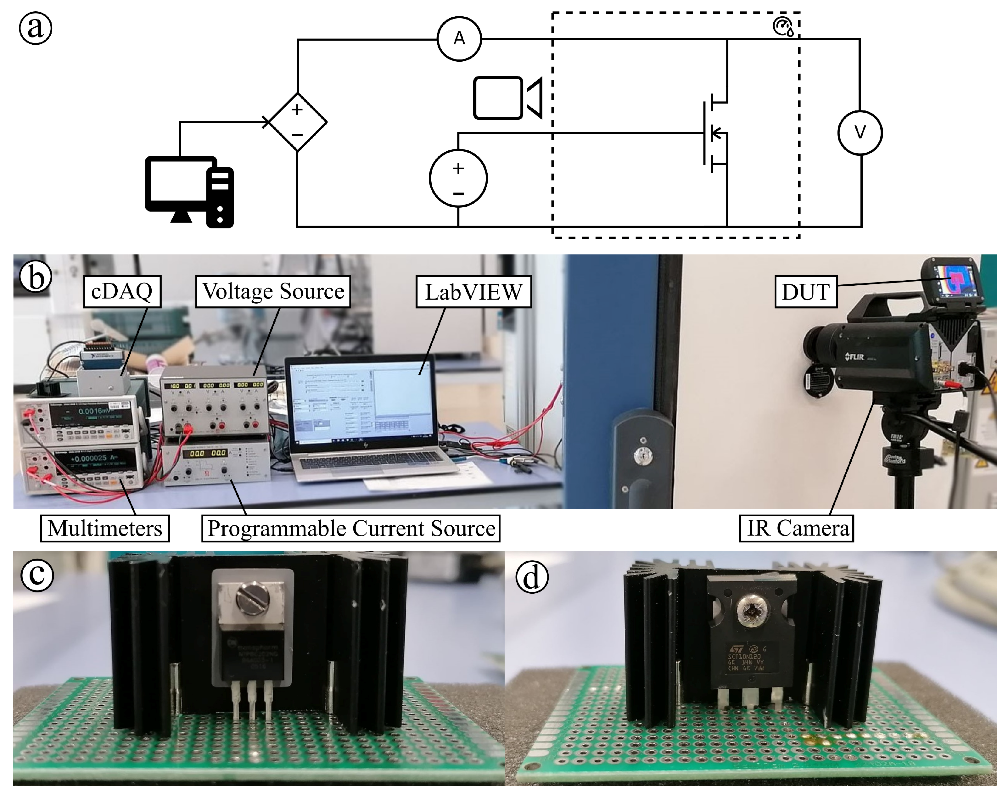
In order to validate the amount of heat generated by the MOSFETs through their power losses, an experimental setup, as shown in Figure 2a,b, was built. Because the 1-D thermal network of the previous subsection only consists of the MOSFET power losses as the main heat source, the MOSFET submodel can be extracted and validated separately instead of the entire inverter topology. Therefore, both MOSFETs have been soldered on a separate PCB together with the RA-T2X-25E heat sink, as depicted in Figure 2c,d. The experimental tests consist of measuring the electrical and the thermal steady-state response of the device under test (DUT) under various combinations of input currents and ambient temperatures that range from 0 A–3 A with steps of 0.5 A and 5 °C–65 °C with steps of 10 °C, respectively, as illustrated in Figure 3. The setup is regulated while using LabVIEW (2019 SP1, National Instruments, Austin, TX, USA) by sending output signals to the programmable current source through a cDAQ and the WEISS climate chamber whilst simultaneously receiving measurements from the Tektronix DMM4050 multimeters and the FLIR X6580SC infrared (IR) camera. An additional constant voltage source is used in order to turn the MOSFETs on by providing 10 V to the GaN MOSFET and 20 V to the SiC MOSFET according to the gate voltage range that was provided by the datasheets. The electrical response in the form of total power losses will be used to validate the MOSFET losses model used in the electro-thermal full-bridge inverter model, while the thermal response in the form of MOSFET case temperatures will be used to validate the FEM model in Section 4.2.
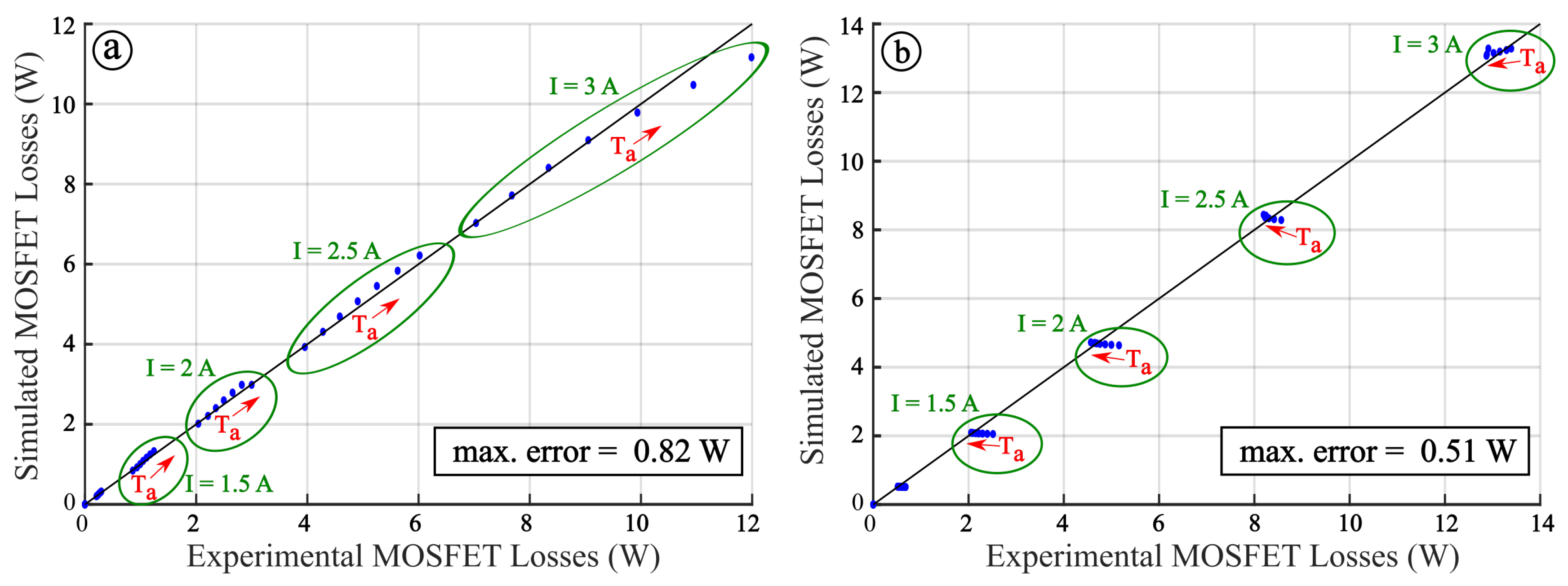
The comparison of power losses between the experimental tests and the simulated results can be seen in Figure 4 for both MOSFETs. For every data point, the same combination of input current and ambient temperature was used as previously mentioned. There is a larger spread in points for the GaN MOSFET across the 45° bisector of the graph which is caused by the increased sensitivity of the on-resistance to temperature. The maximum error for the GaN MOSFET is 0.82 W at the most stressing input condition of 3 A and 65 °C with an underestimation of the simulated losses. This can be caused by another parasitic resistance that was not included in the model, such as a soldering or wiring resistance. On the other hand, the on-resistance of the SiC MOSFET is less sensitive to temperature, according to its datasheet. The maximum error for the SiC MOSFET is 0.52 W and occurs at the input condition of 1.5 A and 2 A. The measurements of the on-resistance during the experiment indicate that the on-resistance actually is inversely proportional to the temperature in this first half of the power losses which is contradictory to its datasheet. This difference between the experimental and the simulated behavior in the lower half of the power losses can be seen in Figure 4b when looking at the direction of increasing ambient temperature. When nearing the end of the graph, this difference tends to disappear because the semiconductor conduction behavior changes towards metallic conduction behavior at higher junction temperatures that does mirror the simulation. Although this semiconductor behavior is not included in the simulations, because it was not included in the datasheet, its effect on the thermo-mechanical stress is insignificant, because it only occurs at lower temperatures where there is negligible deformation occurring in the component.

3. Reverse Engineering Wide-Bandgap Devices

A reverse engineering analysis is performed because the datasheets of both MOSFETs lack very detailed information regarding the internal geometry, dimensions, and composition of the various internal component elements. This is performed using X-ray imaging, scanning electron microscopy (SEM), and energy-dispersive X-ray spectroscopy (EDX). These properties will then be used to create a highly detailed FEM model of both MOSFETs in Section 4 in order to evaluate the plastic deformation that occurs in the different material layers.

3.1. X-ray Imaging

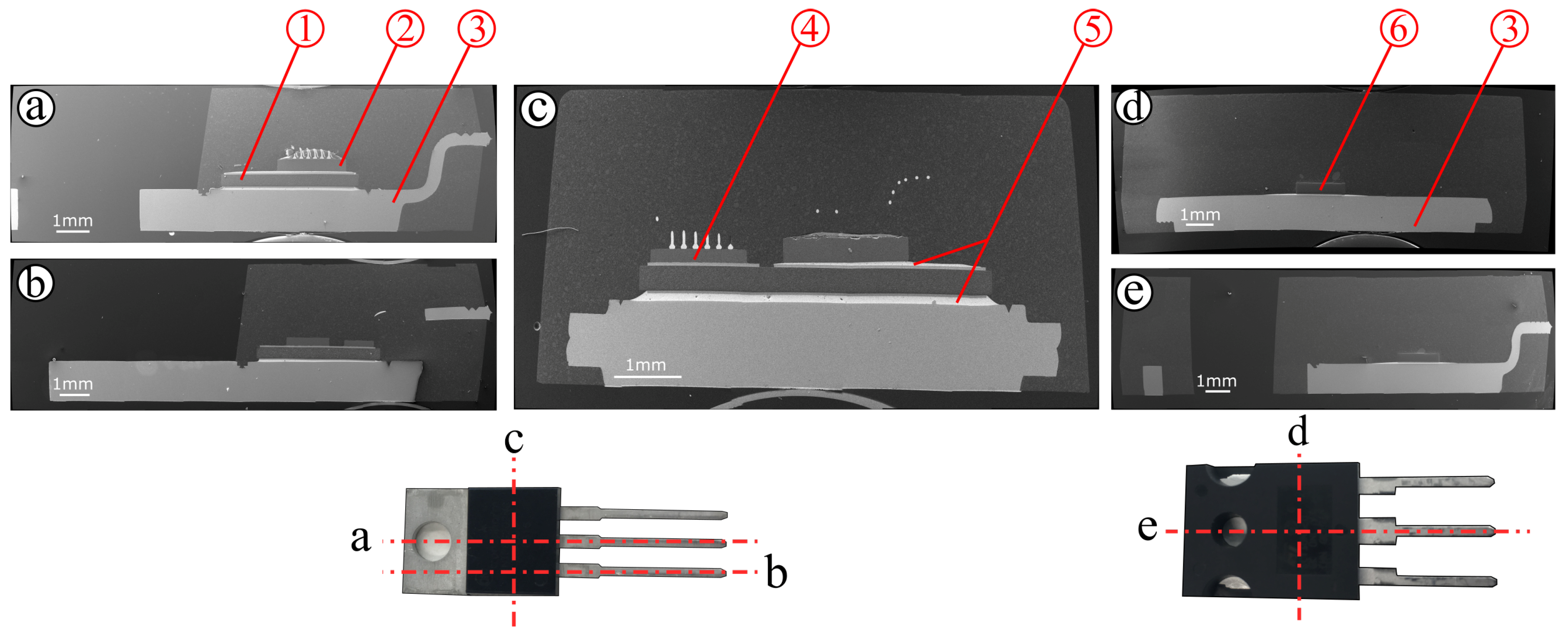
In a first step, X-ray radiography (Phoenix X-ray nanofocus pcba analyser) is performed on both MOSFETs, so that the location of various internal component elements with a different X-ray absorption due to differences in dimensions, density and composition can be visualized [26]. This non-destructive method is fast, but it does not produce enough information to build an accurate FEM model. Based upon the X-ray radiography results, the position of several cross-sections for a SEM-EDX (scanning electron microscopy–energy dispersive X-ray) analysis is defined. The X-ray images of both MOSFETs are depicted in Figure 5. It can be seen that the GaN MOSFET has three dies in agreement with its cascode topology and a parallel interconnection configuration of six Au bond wires. The SiC MOSFET only contains a singular die in the centre. The present Al bond wires absorb too less X-rays to generate a detectable contrast in the X-ray images.

3.2. Scanning Electronic Microscopy and Energy-Dispersive X-Ray Spectroscopy

After the X-ray imaging, several cross-sections are made in different directions, as indicated on Figure 5. The cross-sections are investigated with a FEI Quanta 200F FEG-SEM that was equipped with an UltraDry silicon drift EDX detector of Thermo Fisher (60 mm2 window) with Pathfinder X-ray microanalysis software. To obtain detailed information of the different internal components of the MOSFETs secondary electron (SE) and back scattered electron (BSE) images are made at high magnification. To visualize the layout/position/dimension of the different internal structures in the cross-section much better those images are stitched together and displayed in Figure 6. The BSE images are generated by the back scattered primary electron beam [27]. The BSE yield is a function of the elemental atomic number (Z contrast) and of the angle between the impinging electron beam and the surface. The higher the atomic number, the more electrons are scattered back. The solid state BSE detector in sum mode of the two segments (A and B) allows for the detection of differences in elemental atomic number and, thus, reveal mainly Z contrast. The composition of the structures with a different BSE yield is determined with the EDX analysis. For the cascode GaN MOSFET, three different cross-sections are made so that the three silicon dies are touched in one or more cross-sections. The various internal structures are encapsulated in a standard TO-220 package. Six parallel bond wires are used to interconnect the outer leads with the gate and source of the device. The thicknesses of the three silicon dies are 130 µm, 250 µm and 380 µm with the latter containing a GaN layer of 20 µm. The substrate and the heat sink have a thickness of 380 µm and 1300 µm, respectively. For the SiC MOSFET the internal structure is less complex so that two cross sections are enough to measure the essential information to build up the accurate FEM model. The SiC die is encapsulated in a HiP247™ package package and with a single bond wire interconnected to the outer leads. The thickness of the silicon carbide die and the heat sink are 400 µm and 1180 µm, respectively.
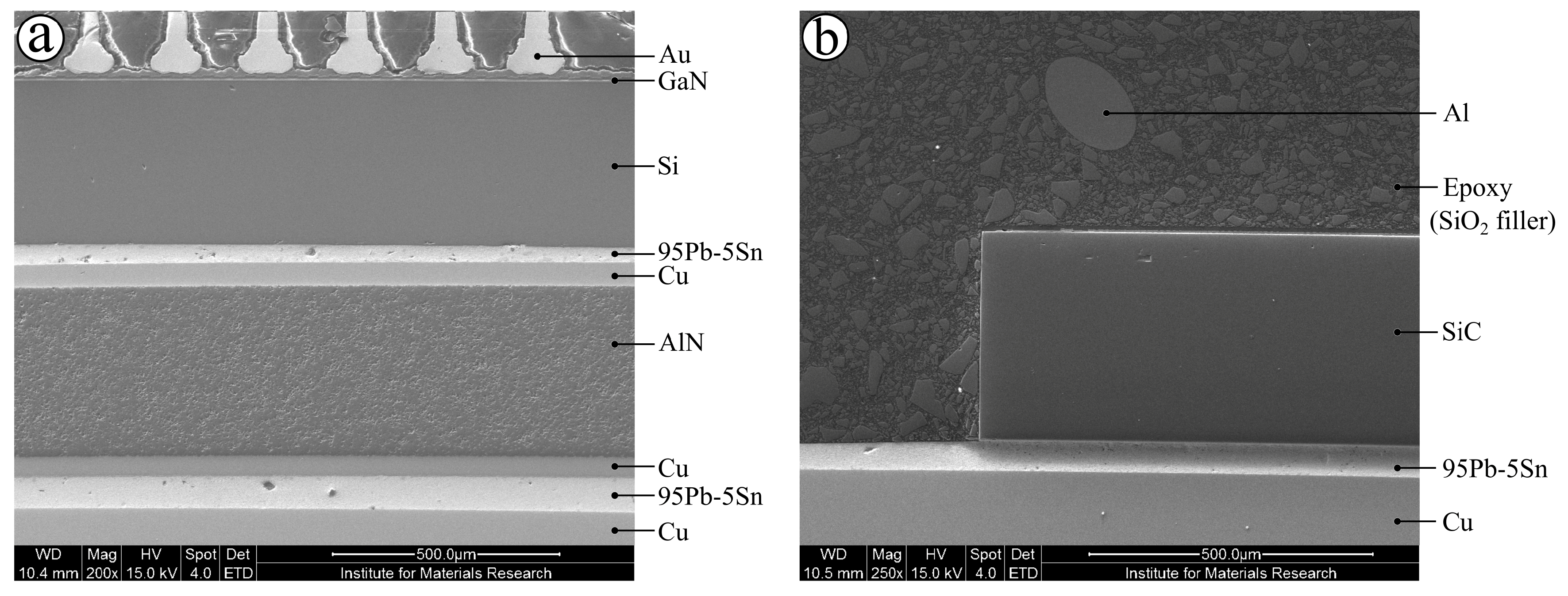
A more detailed image of the Si-AlN (cascode GaN MOSFET) or the SiC (SiC based MOSFET) dies is given in Figure 6. The GaN device (Figure 7a) is comprised of more material layers, because of the multiple dies that are soldered onto a direct bonded copper substrate that consists of AlN in the centre with a sheet of Cu bonded on each side. This substrate is then soldered onto the Cu baseplate using 95Pb-5Sn solder. Gold is the material used for the bond wires and as mentioned before, there is a thin GaN layer of 20 µm on top of the Si die. In the SiC device (Figure 7b), the die is directly soldered onto the Cu baseplate and utilizes Al bond wires. Both devices are encapsulated in an epoxy molding compound (EMC) with a SiO2 filler and use 95Pb-5Sn solder to attach the material layers. The properties of these materials can be extracted from a material database such as CES Edupack (2019, Granta Design, Cambridge, UK) and they are listed in Table 3. The considerable differences in coefficients of thermal expansion (CTE) of the dies, the solder and the bond wires will create significant thermal stress between these materials.

4. Finite Element Method Modeling of Wide-Bandgap Devices

In this section, the information obtained from the previous section that contains the components’ structure, dimensions and materials is used to construct a highly detailed 3D FEM model. Furthermore, the degrees of freedom in this model are increased until convergence is achieved. Finally, the model is validated while using the experimental thermal responses gathered from Section 2.2.

4.1. FEM MOSFET Model Construction

After obtaining the materials and dimensions of the internal structure of both components, the external packaging dimensions can be extracted from their respective datasheet. This allows for the construction of a 3D CAD model of both WBG devices in COMSOL (5.3, COMSOL AB, Stockholm, Sweden), which are rendered see-through in Figure 8 together with an RA-T2X-25E heat sink, a silicone rubber thermal interface, and the FR-4 test board PCB used in the validation of Section 2.2. The heat transfer physics in the form of conductive, convective, and radiative heat transfer are also added for every different material layer. Each material primarily behaves as a linear elastic material based on their respective Young’s Modulus and Poisson’s ratio provided in Table 3. Additionally, the traditional Johnson–Cook constitutive material model [28] is used to model the plastic behavior of the gold and aluminum bond and the 95Pb-5Sn die attach. The plastic behavior of the copper leads and baseplate can also be added to the model, but this is left out due not being a failure-prone part of the component. The parameters used in the plastic models can be found in [29,30,31,32,33]. In order to more realistically model the strain rate dependent behavior of the 95Pb-5Sn solder, the ANAND model can also be implemented [34]. However, this will greatly increase the computation time of the already complex FEM models and additional sub-models of the solder layers might be required that will be focused on in future work. Lastly, fixed constraints are added on the leads of the devices, as they are through-hole and form the only mechanical connection with the PCB.
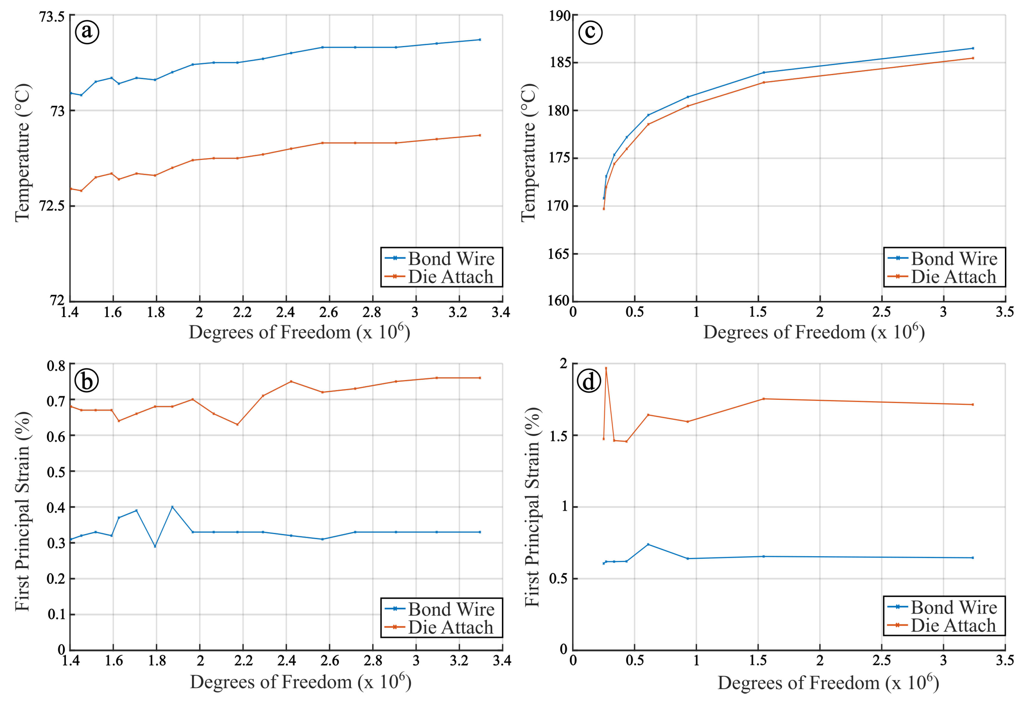
The initial mesh is constructed using a rough tetrahedral volume mesh of the components with a minimum element size of 0.1 mm for the main points of interest such as the bond wires and the die attach and a minimum element size of 3 mm for the rest of the component. The mesh convergence plots that are depicted in Figure 9 can be obtained by gradually decreasing the scale of the entire mesh until convergence is achieved while monitoring several variables. This is done in order to check the accuracy of the model in function of the number of degrees of freedom. The process depends on the chosen variables as well as on the different areas that are scaled down. In this case, the main variables are the first principal strain and the temperature of the bond wires and the die attach as the comparison of Section 5 is based on the plastic dissipation density. A steady-state load of 8 W and 10 W is applied inside the die of the GaN MOSFET and the SiC MOSFET, respectively, at an ambient temperature of 25 °C in order to induce a sufficient amount of principal strain and temperature. Although the temperature and first principal strain of only one bond-wire is displayed in Figure 9, convergence for every bond wire was obtained at the same number of degrees of freedom. For the GaN device, this is achieved at around 2.6 million degrees of freedom, while for the SiC device it is approximated at 3.3 million degrees of freedom due to a lack of RAM. A personal computer with 8 cores at 3.6 GHz and 16 GB RAM was used to perform the aforementioned simulations.

4.2. MOSFET Losses Thermal Model Validation

In order to validate the constructed FEM models of both WBG devices, the component case temperatures that were extracted from the validation experiment of Section 2.2 will be used. In this experiment, a wide range of combinations of junction losses and ambient temperature is applied to the device under test whilst simultaneously monitoring the thermal response. The components were painted black with a thermographic IR spray in order to acquire a uniform emissivity over the surface. This means that only a single temperature conversion is required from the infrared camera in order to measure the actual case temperature. The component case temperatures are logged at steady-state while using a FLIR X6580sc infrared camera with a resolution of 640 by 512 pixels in combination with an infrared window mounted in the door of the climate chamber as done in a previous publication [25]. The junction losses and the ambient temperatures from Section 2.2 were also applied to the FEM model and the resulting simulated case temperatures were compared with the experimentally measured case temperatures in Figure 10. A maximum error of 1.38 °C and 1.95 °C is determined for the GaN MOSFET and the SiC MOSFET, respectively. Reducing this error in the future can potentially be done by including more detailed material models with temperature dependent thermal and mechanical properties at the cost of an increase in computation time.

5. Mission-Profile Based Thermo-Mechanical FEM Simulations of Wide-Bandgap Devices

In this final section before the conclusion is drawn, the constructed and validated FEM models are stressed by two one-hour mission profiles in order to compare the two designs in terms of generated thermo-mechanical stress. These mission profiles, which include a cloudy hour and a clear hour from Arizona, are first translated into a junction losses profile for both components using the electro-thermal string inverter model from Section 2. Afterwards, these losses are applied to the die of the MOSFET while using the same ambient temperature profile. Finally, the plastic energy dissipation density of the die attach and the bond wires of both designs are analyzed and the potential design adaptations are discussed.

5.1. Mission-Profile Translation

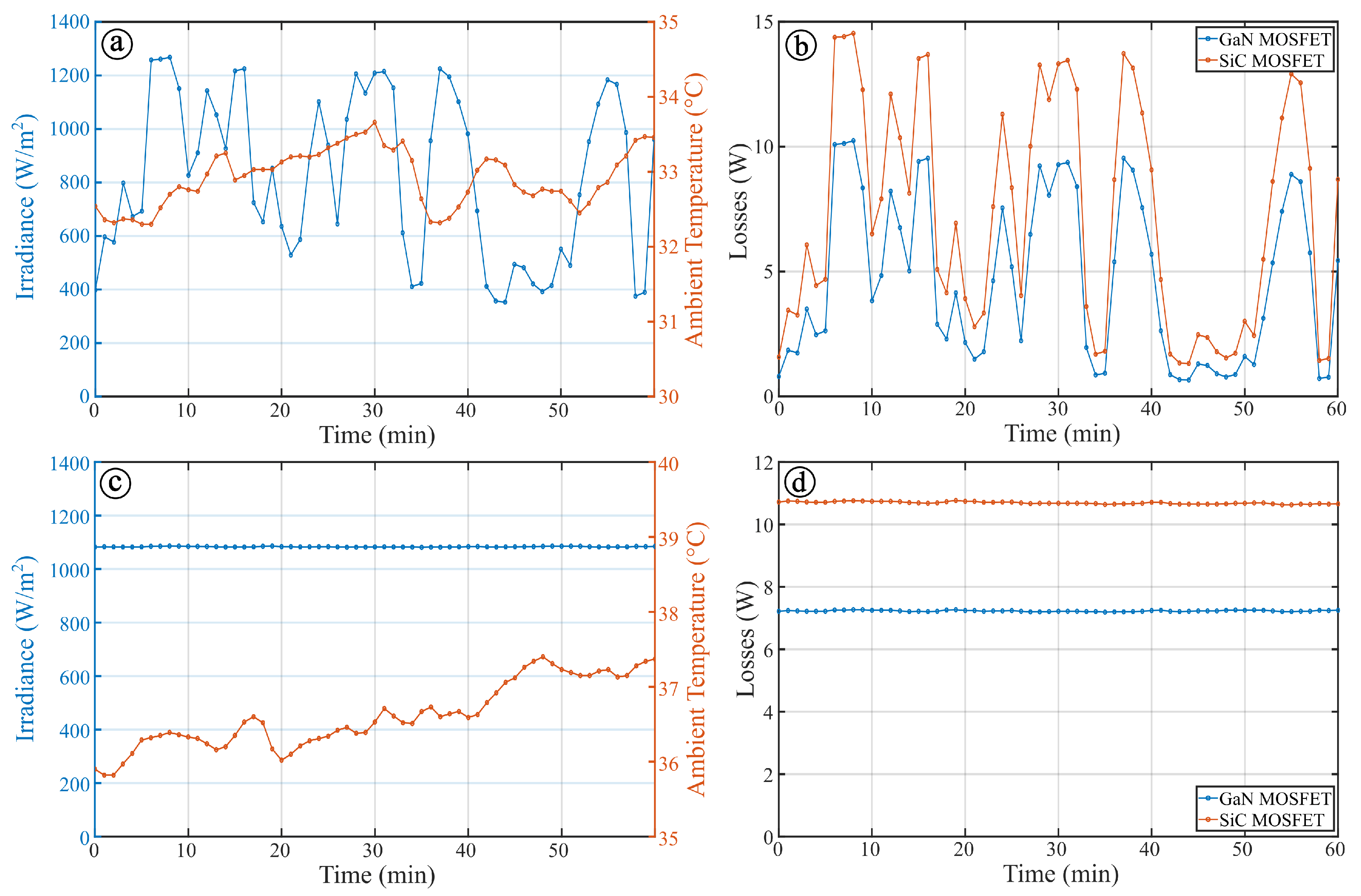
A thorough comparison between the two devices can be achieved using two different mission profiles to stress them. Both of the profiles are from Arizona as it provides a high mean ambient temperature and high levels of irradiance which will induce sufficient thermo-mechanical stress inside the components. On one hand, a cloudy warm hour has been selected with irradiance levels varying from 350 W/m2 to 1300 W/m2 and on the other hand, a clear warm hour has been selected with a nearly constant irradiance of 1075 W/m2. The sample time used in these profiles is one minute and the choice of only using one hour is based on keeping the total computation time within the limits of 10 hours. In order to further investigate the influence of thermal cycles consisting of longer periods, it is recommended to take a 12-hour profile. The next step consists of translating the solar mission profiles into junction losses profiles by using the electro-thermal string inverter model from Section 2. A steady-state lookup table is constructed of the junction losses of both components in function of the ambient temperature and the irradiance of the solar panel. Subsequently, for every point, both one-hour profiles are translated into the losses profiles that are displayed in Figure 11. As predicted by looking at the datasheets of the components, a significant discrepancy in generated losses can be seen between both MOSFETs with a maximum difference of 4 W.

5.2. Thermo-Mechanical FEM Simulation

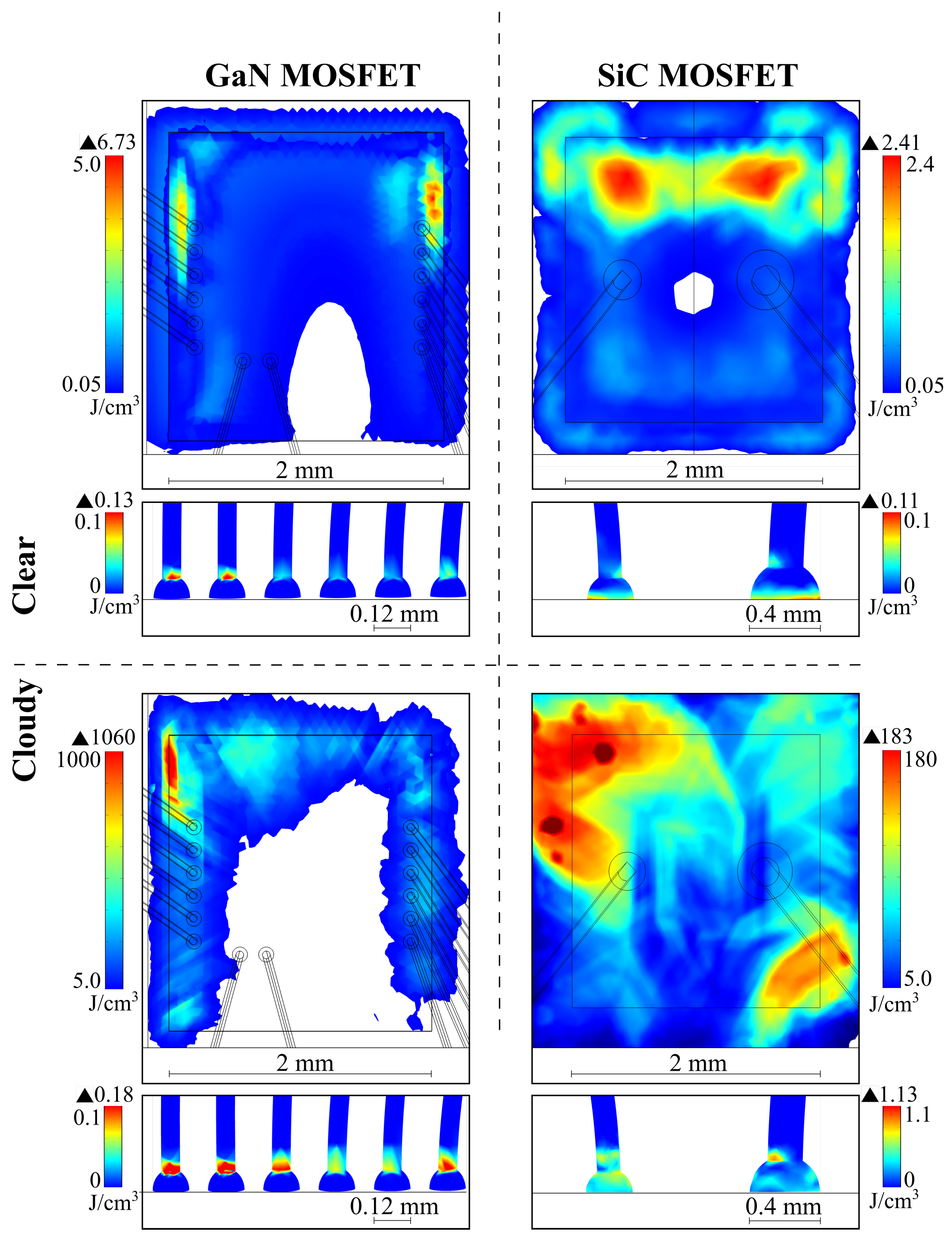
The final step in this methodology consists of applying the obtained one-hour losses profiles onto the FEM models in order to analyze the generated thermo-mechanical stress in the failure-prone areas. The junction losses are injected as a heat source on top of the GaN die and the SiC die, whilst the package, the heat sink, and the PCB are simultaneously surrounded by the corresponding ambient temperature extracted from the mission profile. Additionally, a convective heat transfer coefficient of 35 W/m2 is applied to the natural convective air flow that cools down the external surfaces. The surface plots of the plastic energy dissipation density in the die attach and the bond wires of both components are depicted in Figure 12 for both one-hour profiles. These plots are an efficient way to graphically represent the weak points inside of a component and to potentially make design adaptations in the next iteration of this methodology. There are many conclusions that can be drawn by only looking at the different color scales as the difference in plastic energy dissipation density between a clear and cloudy hour in both cases changes with a factor of 200 and 70 for the GaN MOSFET and the SiC MOSFET, respectively. This means that the temperature amplitude of the thermal cycles are indeed the main source of damage and not the mean temperature. It is also clear that the die attach is undergoing the most amount of plastic deformation. A crack initiation and propagation model is required in order to further analyze the damage in this area and eventually predict the time to failure. However, this falls out of the scope of this paper as the main focus lies on only comparing the generated thermo-mechanical stress. When looking horizontally in Figure 12, the difference between the two devices in terms of plastic energy dissipation density in the 95Pb-5Sn die attach differs with a factor of 2 on clear hour and a factor of 5.5 on a cloudy hour. Even though the GaN MOSFET generates less losses, its smaller packaging and, therefore, reduced available surface to dissipate the heat causes more plastic deformation. For the bond wires, the differences on a clear hour are less distinct. However, the plastic energy dissipation density in the Al wires rises by a factor of 10 on a cloudy day while for the Au wires this only increases with a factor of 1.5. It should be noted that, without the corresponding damage models, an appropriate comparison can only be made between the die attaches of both devices due to being the same material or when looking at the influence of a different mission profile on one device.
After analyzing the surface plots of Figure 12 and determining which component best fits the application, some potential design adaptations can be suggested in order to start a new iteration in the design for reliability methodology. One can either try to increase the packaging size of the GaN device to increase the available surface for heat transfer. Another option could include varying the material used for the die attach in both cases in order to determine the trade-off between electrical resistivity, and therefore efficiency, and reliability. Finally, the effect of multiple parallel bond wires instead of one singular bond wire can also be investigated further. As an extension to this paper, the latter has been simulated in which the aluminum bond wire of the SiC MOSFET with a diameter of 200 µm is exchanged with four parallel wires with a diameter of 50 µm and a spacing of 300 µm. Even though using four smaller wires introduces some redundancy for the failure of a single wire, the simulated plastic energy dissipation density is eight times higher when applying the cloudy one-hour mission profile than when using only a single thick wire. This methodology allows for similar trade-offs to be simulated in a short time frame in comparison with the lengthier traditional accelerated stress testing. Ultimately, after several iterations, a design with an optimal combination of compactness, reliability and efficiency can be achieved, constructed, and implemented.

6. Conclusions

In this paper, a thermo-mechanical stress comparison between two commercially available wide-bandgap devices was performed when used in the same photovoltaic application as a first iteration in the design for reliability methodology. Firstly, an electro-thermal model of a photovoltaic string inverter was constructed and validated in order to translate a solar mission profile into a junction losses profile. Secondly, the structure, dimensions and material compositions of the internal and external structure of both devices were extracted while using X-ray imaging, scanning electron microscopy, and energy dispersive X-ray spectroscopy, respectively. Thirdly, while using the gathered input from the previous step, finite element method models of the cascode GaN MOSFET and the SiC MOSFET were constructed and validated. Finally, a cloudy and a clear one-hour mission profile from Arizona was applied to the FEM models in order to compare the generated thermo-mechanical stress in the die attach and the bond wires. The results showed that the deformation generated in the die attach by a cloudy mission-profile is 200 times and 70 times more than a clear mission-profile for the GaN MOSFET and the SiC MOSFET, respectively, which means that the amplitudes of the thermal cycles are the main source of damage. The GaN MOSFET, in spite of its reduced losses, endured two times on a clear hour and 5.5 times on a cloudy hour more deformation in its die attach than the SiC MOSFET due to its lower available surface for heat dissipation. In comparison with the die attach, the deformation in the bond wires is less noticeable for a clear hour. However, when looking at the results for the cloudy hour, the aluminum wires are more susceptible to thermal cycling than the gold wires as their plastic dissipation density increases by a factor of 10 compared to a factor of 1.5. Corresponding damage models are required in order to make additional comparisons between different materials. Potential design adaptations in order to start a new iteration in the design for reliability methodology can include increasing the packaging size of the GaN MOSFET, testing different die attach materials, or varying the amount of parallel bond wires.

Author Contributions

Conceptualization, W.V.D.S.; Data curation, J.D. and M.D.; Formal analysis, W.V.D.S. and M.D.; Funding acquisition, M.D.; Investigation, W.V.D.S. and M.D.; Methodology, W.V.D.S.; Project administration, M.D.; Resources, P.N., J.D. and M.D.; Software, W.V.D.S., O.A., P.N. and M.D.; Supervision, M.D.; Validation, W.V.D.S.; Visualization, W.V.D.S.; Writing—original draft, W.V.D.S.; Writing—review & editing, O.A., J.D. and M.D. All authors have read and agreed to the published version of the manuscript.

Funding

This research and the APC were funded by the project Rolling Solar, executed within the framework of the cross border collaboration program Interreg Euregio Meuse-Rhine V-A with financial support of the European Regional Development Fund.

Acknowledgments

The authors would like to thank the lab technicians of Hasselt University and imec for assisting with the experimental testing.

Conflicts of Interest

The authors declare no conflict of interest.

References

  1. Breyer, C.; Bogdanov, D.; Aghahosseini, A.; Gulagi, A.; Child, M.; Oyewo, A.S.; Farfan, J.; Sadovskaia, K.; Vainikka, P. Solar photovoltaics demand for the global energy transition in the power sector. Prog. Photovolt. Res. Appl. 2018, 26, 505–523. [Google Scholar] [CrossRef]
  2. Rakhshani, E.; Rouzbehi, K.; del Pozo Fernandez, A.J.S.; Cabrera-Tobar, A.; Pouresmaeil, E. Integration of Large Scale PV-Based Generation into Power Systems: A Survey. Energies 2019, 12, 1425. [Google Scholar] [CrossRef] [Green Version]
  3. Apostoleris, H.; Sgouridis, S.; Stefancich, M.; Chiesa, M. Utility solar prices will continue to drop all over the world even without subsidies. Nat. Energy 2019, 4, 833–834. [Google Scholar] [CrossRef] [Green Version]
  4. Mehravaran, A.; Derhem, A.; Nassereddine, M. Building-Integrated Photovoltaics (BIPV) for Residential and Industrial Properties. In Proceedings of the 2019 Advances in Science and Engineering Technology International Conferences (ASET), Dubai, UAE, 26 March–10 April 2019; IEEE: Dubai, UAE, 2019; pp. 1–6. [Google Scholar] [CrossRef]
  5. Sarkar, D.; Kumar, A.; Sadhu, P.K. A Survey on Development and Recent Trends of Renewable Energy Generation from BIPV Systems. IETE Tech. Rev. 2020, 37, 258–280. [Google Scholar] [CrossRef]
  6. Quintana, S.; Huang, P.; Saini, P.; Zhang, X. A preliminary techno-economic study of a building integrated photovoltaic (BIPV) system for a residential building cluster in Sweden by the integrated toolkit of BIM and PVSITES. Intell. Build. Int. 2020, 1–19. [Google Scholar] [CrossRef]
  7. Zhang, Y.; Zhao, G.; Wu, Y.; Liu, C. Optimal planning of building integrated photovoltaic system in urban energy internet. In Proceedings of the 2017 IEEE Conference on Energy Internet and Energy System Integration (EI2), Beijing, China, 26–28 November 2017; IEEE: Beijing, China, 2017; pp. 1–6. [Google Scholar] [CrossRef]
  8. Dobrzycki, A.; Kurz, D.; Mikulski, S.; Wodnicki, G. Analysis of the Impact of Building Integrated Photovoltaics (BIPV) on Reducing the Demand for Electricity and Heat in Buildings Located in Poland. Energies 2020, 13, 2549. [Google Scholar] [CrossRef]
  9. Zhang, T.; Wang, M.; Yang, H. A Review of the Energy Performance and Life-Cycle Assessment of Building-Integrated Photovoltaic (BIPV) Systems. Energies 2018, 11, 3157. [Google Scholar] [CrossRef] [Green Version]
  10. Arai, J.; Iba, K.; Funabashi, T.; Nakanishi, Y.; Koyanagi, K.; Yokoyama, R. Power electronics and its applications to renewable energy in Japan. IEEE Circuits Syst. Mag. 2008, 8, 52–66. [Google Scholar] [CrossRef]
  11. Chakraborty, S.; Simões, M.G.; Kramer, W.E. (Eds.) Power Electronics for Renewable and Distributed Energy Systems: A Sourcebook of Topologies, Control and Integration; Green Energy and Technology; Springer: London, UK, 2013; OCLC: 855561950. [Google Scholar]
  12. Rezk, H.; Eltamaly, A.M. A comprehensive comparison of different MPPT techniques for photovoltaic systems. Sol. Energy 2015, 112, 1–11. [Google Scholar] [CrossRef]
  13. Falck, J.; Felgemacher, C.; Rojko, A.; Liserre, M.; Zacharias, P. Reliability of Power Electronic Systems: An Industry Perspective. IEEE Ind. Electron. Mag. 2018, 12, 24–35. [Google Scholar] [CrossRef] [Green Version]
  14. De León-Aldaco, S.E.; Calleja, H.; Chan, F.; Jiménez-Grajales, H.R. Effect of the Mission Profile on the Reliability of a Power Converter Aimed at Photovoltaic Applications—A Case Study. IEEE Trans. Power Electron. 2013, 28, 2998–3007. [Google Scholar] [CrossRef]
  15. Petrone, G.; Spagnuolo, G.; Teodorescu, R.; Veerachary, M.; Vitelli, M. Reliability Issues in Photovoltaic Power Processing Systems. IEEE Trans. Ind. Electron. 2008, 55, 2569–2580. [Google Scholar] [CrossRef]
  16. Sintamarean, C.; Eni, E.; Blaabjerg, F.; Teodorescu, R.; Wang, H. Wide-band gap devices in PV systems—Opportunities and challenges. In Proceedings of the 2014 International Power Electronics Conference (IPEC-Hiroshima 2014-ECCE ASIA), Hiroshima, Japan, 18–21 May 2014; IEEE: Hiroshima, Japan, 2014; pp. 1912–1919. [Google Scholar] [CrossRef]
  17. Singh, R. Reliability and performance limitations in SiC power devices. Microelectron. Reliab. 2006, 46, 713–730. [Google Scholar] [CrossRef]
  18. Roccaforte, F.; Fiorenza, P.; Greco, G.; Lo Nigro, R.; Giannazzo, F.; Iucolano, F.; Saggio, M. Emerging trends in wide band gap semiconductors (SiC and GaN) technology for power devices. Microelectron. Eng. 2018, 187–188, 66–77. [Google Scholar] [CrossRef]
  19. She, X.; Huang, A.Q.; Lucia, O.; Ozpineci, B. Review of Silicon Carbide Power Devices and Their Applications. IEEE Trans. Ind. Electron. 2017, 64, 8193–8205. [Google Scholar] [CrossRef]
  20. Wang, J.; Jiang, X. Review and analysis of SiC MOSFETs’ ruggedness and reliability. IET Power Electron. 2020, 13, 445–455. [Google Scholar] [CrossRef]
  21. Ceccarelli, L.; Kotecha, R.M.; Bahman, A.S.; Iannuzzo, F.; Mantooth, H.A. Mission-Profile-Based Lifetime Prediction for a SiC mosfet Power Module Using a Multi-Step Condition-Mapping Simulation Strategy. IEEE Trans. Power Electron. 2019, 34, 9698–9708. [Google Scholar] [CrossRef]
  22. Sintamarean, N.; Wang, H.; Blaabjerg, F.; Rimmen, P.P. A design tool to study the impact of mission-profile on the reliability of SiC-based PV-inverter devices. Microelectron. Reliab. 2014, 54, 1655–1660. [Google Scholar] [CrossRef]
  23. Blaabjerg, F.; Zhou, D.; Sangwongwanich, A.; Wang, H. Design for reliability in renewable energy systems. In Proceedings of the 2017 International Symposium on Power Electronics (Ee), Novi Sad, Serbia, 19–21 October 2017; pp. 1–6. [Google Scholar] [CrossRef]
  24. Graovac, D.; Pürschel, M.; Kiep, A. MOSFET Power Losses Calculation Using the Data-Sheet Parameters; Technical Report; Newark element14; Infineon Technologies AG: Chicago, IL, USA, 2006. [Google Scholar]
  25. Van De Sande, W.; Ravyts, S.; Alavi, O.; Nivelle, P.; Driesen, J.; Daenen, M. The Sensitivity of an Electro-Thermal Photovoltaic DC–DC Converter Model to the Temperature Dependence of the Electrical Variables for Reliability Analyses. Energies 2020, 13, 2865. [Google Scholar] [CrossRef]
  26. Novelline, R.A.; Squire, L.F. Squire’s Fundamentals of Radiology, 5th ed.; Harvard University Press: Cambridge, MA, USA, 1997. [Google Scholar]
  27. Goldstein, J. (Ed.) Scanning Electron Microscopy and X-ray Microanalysis, 3rd ed.; Kluwer Academic/Plenum Publishers: New York, NY, USA, 2003. [Google Scholar]
  28. Li, T.; Zhao, B.; Lu, X.; Xu, H.; Zou, D. A Comparative Study on Johnson Cook, Modified Zerilli–Armstrong, and Arrhenius-Type Constitutive Models to Predict Compression Flow Behavior of SnSbCu Alloy. Materials 2019, 12, 1726. [Google Scholar] [CrossRef] [Green Version]
  29. Zein, H.; Irfan, O. Surface Roughness Investigation and Stress Modeling by Finite Element on Orthogonal Cutting of Copper. Metals 2018, 8, 418. [Google Scholar] [CrossRef] [Green Version]
  30. Hu, Y.; Kumar, P.; Xu, R.; Zhao, K.; Cheng, G.J. Ultrafast direct fabrication of flexible substrate-supported designer plasmonic nanoarrays. Nanoscale 2016, 8, 172–182. [Google Scholar] [CrossRef] [PubMed]
  31. Manikam, V.R.; Cheong, K.Y. Die Attach Materials for High Temperature Applications: A Review. IEEE Trans. Compon. Packag. Manuf. Technol. 2011, 1, 457–478. [Google Scholar] [CrossRef]
  32. Bressan, J.D.; Lopez, K. New constitutive equation for plasticity in high speed torsion tests of metals. Int. J. Mater. Form. 2008, 1, 213–216. [Google Scholar] [CrossRef]
  33. Khatibi, G.; Betzwar Kotas, A.; Lederer, M. Effect of aging on mechanical properties of high temperature Pb-rich solder joints. Microelectron. Reliab. 2018, 85, 1–11. [Google Scholar] [CrossRef]
  34. Long, X.; Chen, Z.; Wang, W.; Fu, Y.; Wu, Y. Parameterized Anand constitutive model under a wide range of temperature and strain rate: Experimental and theoretical studies. J. Mater. Sci. 2020, 55, 10811–10823. [Google Scholar] [CrossRef]
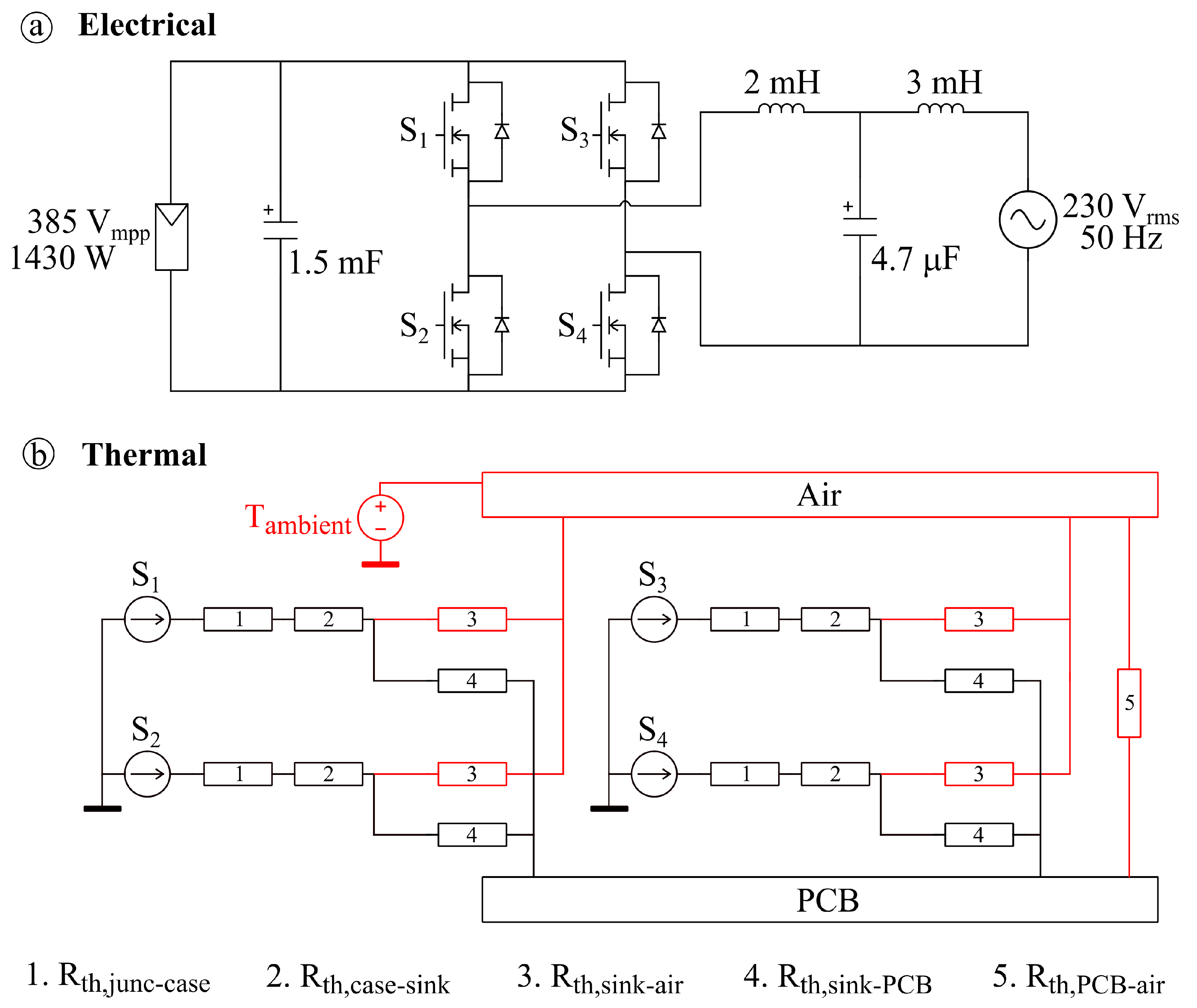
Figure 1. (a) The electrical circuit of a photovoltaic full-bridge inverter and (b) the equivalent one-dimensional (1-D) steady-state Foster thermal network for the semiconductor devices with the conductive (black) and the convective (red) heat transfer path.
Energies 13 05900 g001
Figure 2. (a) The schematic and (b) photo of the experimental setup to validate the power losses model of the (c) cascode gallium nitride (GaNO) metal-oxide-semiconductor field-effect transistors (MOSFET) and the (d) silicon carbide (SiC) MOSFET.
Energies 13 05900 g002
Figure 3. The current (A) and ambient temperature (°C) profile used as the input for the experimental validation setup that is shown in Figure 2.
Energies 13 05900 g003
Figure 4. The experimental and the simulated steady-state power losses of the (a) cascode GaN MOSFET and the (b) SiC MOSFET when loaded by the same input conditions.
Energies 13 05900 g004
Figure 5. X-ray imaging of the (a,b) GaN cascode MOSFET and the (c,d) SiC MOSFET with the (1)–(5) cross-sections made for the SEM.
Energies 13 05900 g005
Figure 6. Scanning electron microscopy cross section images of (ac) a cascode GaN device and (d,e) a SiC device with (1) the ceramic substrate, (2) the GaN-on-Si die, (3) the baseplate, (4) the anti-parallel diode, (5) the solder interconnection, and (6) the SiC die.
Energies 13 05900 g006
Figure 7. Scanning electron microscopy cross section images of (a) a cascode GaN device and (b) a SiC device with the respective material layers
Energies 13 05900 g007
Figure 8. 3D CAD model of (a) the cascode GaN MOSFET and (b) the SiC MOSFET mounted on a PCB with the RA-T2X-25E heat sink.
Energies 13 05900 g008
Figure 9. Convergence plots of the (a,c) temperature and the (b,d) first principal strain of the cascode GaN MOSFET and the SiC MOSFET respectively.
Energies 13 05900 g009
Figure 10. The experimental and the simulated steady-state MOSFET case temperature of the (a) cascode GaN MOSFET and the (b) SiC MOSFET when loaded by the same input conditions.
Energies 13 05900 g010
Figure 11. Translating a (a,b) one-hour cloudy mission profile and (c,d) a one-hour clear mission profile of Arizona into the corresponding junction losses profile of the used MOSFET.
Energies 13 05900 g011
Figure 12. Plastic energy dissipation density surface plots of the die attach and bond wires of the GaN MOSFET and the SiC MOSFET after being stressed by the one-hour mission profiles from Figure 11.
Energies 13 05900 g012
Table 1. The extracted or calculated values of the thermal resistances used in the 1-D steady state Foster network of Figure 1b for both wide-bandgap devices.
NumberThermal ResistanceGaN Cascode MOSFETSiC MOSFET
1Junction-to-Case (Rth,junc-case)2.3 K/W1.17 K/W
2Case-to-Heatsink (Rth,case-sink)0.69 K/W
3Heatsink-to-Air (Rth,sink-air)3.06 K/W
4Heatsink-to-PCB (Rth,sink-PCB)13.25 K/W
5PCB-to-Air (Rth,PCB-air)9.5 K/W
Table 2. The wide-bandgap devices used in the photovoltaic full-bridge inverter together with their key parameters.
GaN Cascode MOSFETSiC MOSFET
ManufacturerON SemiconductorSTMicroelectronics
CodeNTP8G202NSCT10N120
PackageTO-220HiP247TM
On-resistance at Tj = 25 °C0.290 Ω0.520 Ω
On-resistance at Tj = 150 °C0.580 Ω0.533 Ω
Max. junction operating temperature150 °C200 °C
Drain-source voltage600 V1200 V
Drain current at Tc = 25 °C9 A12 A
Reverse recovery charge29 nC107 nC
Table 3. Properties of the materials detected inside the GaN and SiC MOSFET
MaterialYoung’s Modulus (GPa)Poisson’s RatioThermal Conductivity (W/m·K)Coefficient of Thermal Expansion (K−1)Heat Capacity at Constant Pressure (J/kg·K)
Epoxy resin (SiO2 fill)130.340.623 × 10−61.3 × 10³
Si1600.271302.6 × 10−6700
AlN3200.261205.3 × 10−6800
95Pb-5Sn150.443628.6 × 10−6140
GaN (Wurtzite)2950.231303.2 × 10−6490
Au780.4231514 × 10−6130
SiC4100.23703.5 × 10−6690
Cu1100.3540017 × 10−6385
Al700.3523723.1 × 10−6904
Publisher’s Note: MDPI stays neutral with regard to jurisdictional claims in published maps and institutional affiliations.