Review

A Review on Real-Size Epoxy Cast Resin Insulators for Compact High Voltage Direct Current Gas Insulated Switchgears (GIS) and Gas Insulated Transmission Lines (GIL)—Current Achievements and Envisaged Research and Development

Advanced High Voltage Engineering Research Centre, School of Engineering, Cardiff University, The Parade, Cardiff CF24 3AA, UK
*
Author to whom correspondence should be addressed.
Energies 2020, 13(23), 6416; https://doi.org/10.3390/en13236416
Submission received: 25 October 2020 / Revised: 30 November 2020 / Accepted: 30 November 2020 / Published: 4 December 2020
(This article belongs to the Section F: Electrical Engineering)

Abstract

:
Due to the ever-increasing demand for electricity in the one hand and the environmental constraints to use clean energy on the other hand, the global production of energy from remote renewable sources, particularly from large hydropower plants and offshore wind farms and their connection to the grid are expected to grow significantly in the future. Consequently, the demand to carry this electric power by high voltage direct current (HVDC) technology will increase too. The most suitable HVDC power transmission technology to deliver large amounts of power, exceeding a capacity of 5 GW per bipolar system over long distances with lower losses is by using compact HVDC gas insulated transmission lines (DC GIL) and gas insulated switchgears (DC GIS) with rated voltage (maximum continuous operating voltage) of ±550 kV and 5000 A which are presently under development worldwide. Among the critical challenges for the development of these HVDC gas insulated systems, there are the epoxy cast resin insulators that are used to separate gas compartments also called spacers. Indeed, thorough research studies have been and still being carried out to well understand and clarify the electrical insulation characteristics of HVDC spacers using mainly cylindrical samples and small insulator models, where useful results have been obtained and proposed for implementation in real compact gas insulated systems. However, few practical investigations have been undertaken on real size spacers (product scale) to verify such research outcomes and validate the reliability of the spacers to collect experiences or for commercial use. This paper reviews the current achievements of real size HVDC spacers development. It describes the basic electric field calculation and spacers design, the verification of the insulation performance and validation testing. It gives today’s commercially available compact HVDC GIS/GIL and finally it presents the envisaged future research and development.

1. Introduction

While for high voltage alternating current (HVAC) applications, gas insulated switchgears (GIS) and gas insulated transmission lines (GIL) are well-proven technologies operating under a voltage of at least 800 kV AC, their development for high voltage direct current (HVDC) applications is extremely challenging. Consequently, new compact HVDC GIS and GIL for operation under rated voltage of ±550 kV and higher voltage levels are currently under development worldwide. The main reason of this strong interest is that large electric power generation from renewable sources is projected to accelerate in the future and hence the demand for its transmission from these remote generation sites to high consumption areas is expected to increase. To balance the renewable power generation over a wide area e.g., Europe, it is also necessary to transmit large amount of power from areas where wind or solar energy is available to other regions without. Underground HVDC GIL technology is particularly well-suited to carry very high power of several gigawatts (5 GW) per bipolar system over long distances with very low losses. This applies when overhead lines are not permitted due to their visual impact and public opposition, and when for the same allowable installation space, XLPE extruded HVDC cables cannot be used due to their limited power transmission capacity to about 3 GW per bipolar system with rated voltage of ±640 kV DC [1]. On the other hand, compact HVDC GIS is highly required wherever space saving is an important issue such as in densely populated areas and in offshore wind power converter stations.
Japan is pioneer in the research and development of ±500 kV HVDC GIS which were undertaken for some years in the 1980s. The technical problems were addressed, the appropriate solutions were found, and their effectiveness were validated by tests verification [2,3,4,5] which lead to the worldwide first commercial DC GIS that was installed at Anan converter station for the Kii-Channel HVDC link equipment to connect Honshu and Shikoku by using a submarine power cable [6]. However, this GIS has large dimensions (1 m in diameter) and has been in operation since 2000 at ±250 kV instead. With a regain of interest for HVDC GIS due to the growing demand of HVDC electricity transmission, the focus today is being put on further improvement and development of compact HVDC GIS as published in [7,8,9,10]. Indeed, a new ±250 kV DC GIS has been developed to connect Hokkaido and Honshu where details about the specifications, design and the results of type tests and verification tests are given in [7]. Furthermore, with the acquisition of Hitachi (Tokyo, Japan) of ABB Power Grids (Zurich, Switzerland) this latter has already developed, put in the market the ±320 kV (nominal voltage)/±350 kV (rated voltage) DC GIS [11,12,13] and is now pursuing the development for the ±500 kV (nominal voltage)/±550 kV (rated voltage) DC GIS.
In Europe, Siemens (Munich, Germany) is ahead since compact HVDC switchgears for rated voltages of ±350 kV and ±550 kV [14,15,16] are available in the market [17] for applications on DC offshore converter platforms for wind farms as well as onshore where space is limited. In addition, the development of compact HVDC underground GIL for operation under ±550 kV and up to rated current of 5000 A is completed and this new transmission technology is approaching the market [17,18,19,20,21,22,23].
On the other hand, with the development of ultra-high voltage (UHV) power transmission in China [24] and the growing interest to exploit large hydropower resources from the mountain areas in central China to the load centres in the east, the UHVDC electricity transmission for voltage level ±800 kV and above through compact HVDC GIL/GIS technologies seem promising. Indeed, intensive research on this topic has been recently conducted resulting in a considerable number of published papers such as the works of [24,25,26] and those referred to in this review paper about real size DC spacers.
Epoxy insulators (cone or disc shaped) used to isolate gas compartments in compact HVDC GIS/GIL systems also called spacers are the most critical components responsible for surface flashover, therefore, extensive research studies have been carried out mainly on cylindrical samples and spacer models having small dimensions to well understand and clarify the electrical insulation characteristics of the spacers [24,25,26,27,28,29]. Indeed, new test techniques have been developed for this aim. However, from the practical viewpoint only few investigations have been reported on full/real size spacer components to check concretely the outcomes of these studies. Indeed, there are only the GIS/GIL manufacturers which so far have successfully performed the dielectric testing for the development of their compact ±350 kV and ±550 kV systems.
This review paper summarizes in brief, based on the available literature, the status of the achievements of full-size spacers for the development of compact ±350 kV and ±550 kV HVDC GIS/GIL. The paper is organized as follow. After the introduction presented in Section 1, Section 2 lists the technical challenges for the development of HVDC spacers namely the electric field enhancement caused by their presence, charge accumulation on the spacers’ surface, flashover under superimposed lightning or switching impulse voltage onto the operating DC voltage and the influence of metallic particles’ contamination. Section 3 describes the fundamental theoretical aspects where the mandatory numerical calculations prior spacers fabrication and testing, should be performed with respect to the electric field distribution and surface charges accumulation under the DC operating conditions and all the required qualification tests conditions. The obtained numerical results are given in Section 4. Section 5 describes the practical tests that have been performed to validate the simulation results on real size arrangements by following the required sequence tests specific for HVDC GIS/GIL insulation qualification as well as today’s commercially available products. Section 6 gives some envisioned developments. Finally, Section 7 presents the conclusions.

2. Technical Challenges for the Development of Spacers for Compact HVDC GIS/GIL

GIS bus bar and GIL (Figure 1a,b) [30] have similar basic structure which consists of an inner conductor tube energized at high voltage (HV) surrounded by an outer grounded enclosure tube and the space between them is filled with a pressurized gas. Pure sulfur hexafluoride (SF6) is used in GIS to ensure arc quenching functionality and SF6/N2 gas mixture is used in GIL to provide excellent electric insulation. The GIS/GIL contain solid insulators: (i) post-type insulators are used to hold the HV conductor in the center and (ii) non-gas tight or gas tight insulators where the former type are perforated and employed to fix the conductor towards the enclosure and the latter type to separate the gas compartments also known as spacers. Besides, a trap for mobile metallic particles contaminants is implemented.
Spacers are cast, filled epoxy matrix with alumina (Al2O3), or silica (SiO2). The epoxy matrix is usually composed of a base resin mixed with a hardener and a catalyst. Diglycidyl ether bisphenol A (DGEBA)-based resin and an acid anhydride hardener are among the used materials. Fillers are necessary for good mechanical and thermal properties, as well as for minimal shrinkage during casting. The concentration of the filler is between 60–70% per weight. Alumina-filled epoxy composite appears to be the most suitable material in GIS mainly due to its resistance against SF6 decomposition byproducts. The epoxy composite formulations are, however, proprietary to the GIS/GIL manufacturers.
Spacers are key components and as mentioned previously although they have been developed for HVAC applications, they cannot be used for HVDC applications due to the following major problems.

2.1. Resistive Electric Field Enhancement

Under steady state DC operating voltage, the electric field distribution in the vicinity and along the spacer surface is controlled by the electric conductivity, σ, of the gas and the spacer’s epoxy material according to the relation div(σE) = 0, where σ of the spacer’s epoxy material depends on the electric field (E) and strongly on the temperature (T). When the GIL/GIS is under full load operation, a temperature gradient (ΔT) between the conductor and the enclosure takes place due to the DC current flow and ohmic losses by Joule effect in the conductor. A difference in conductivity is created and as a result, the resistive electric field is intensified in cold regions of the insulation where the DC conductivity is at its minimum.
Furthermore, besides the effect of the spacer’s material electric conductivity, the shape of the spacer and its contacts with the energized (HV) conductor/grounded (GND) enclosure and the surrounding gas called triple junctions, modify also the electric field distribution especially at the triple junctions where it can be significantly intensified. Therefore, a proper design of the spacer’s shape and its triple contacts is necessary to keep the high electric field strength under control and within the permissible level.

2.2. Charges’ Accumulation on the Spacer’s Surface

The accumulation of charges on the spacer’s surface is a very serious problem when the GIS/GIL is subjected to either continuous high DC voltage or polarity reversal because it distorts the electric field distribution along the surface and can lead to a harmful local field enhancement causing an unpredictable surface flashover along the spacer. It is thus very important to understand and clarify the origins of the surface charges’ accumulation in order to limit its amount to an acceptable level.

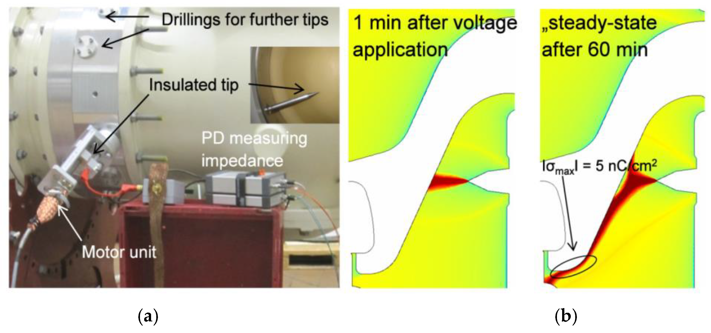
2.3. Flashover under Superimposed Lightning/Switching Impulse Voltage onto DC Operating Voltage

As voltage surges occur in the insulation when HVDC GIS/GIL is switched on and off and under lightning strikes, the accumulated charges on the spacer’s surface during the operating DC voltage tend to lower the surface electric field withstand under these surges. Therefore, to design a reliable HVDC spacer, it must fulfill the required lightning and switching impulse withstand voltage levels (LIWV and SIWV) when they are superimposed on DC voltage [31].

2.4. Metallic Particles

Metallic particles’ contamination inside the GIS/GIL enclosure caused by vibrations during shipment, mechanical abrasions during installation or conductor movement under load cycling, should be avoided for DC application like in the case for HVAC application since it has been clearly proofed, through the extensive Japanese studies in the frame of their ±500 kV GIS development [3,4,5], that these metallic particles have a drastic influence on the GIS/GIL insulation performance not only on the spacer’s surface but on the gas gap insulation as well.
This effect is not covered in this paper as it is assumed that the DC GIS/GIL systems must operate in industrially very clean conditions and the problem of metallic particles inside the enclosure under DC service is solved by the integration of new types of traps different of those of AC. Further details about these problems and the measures to be taken against them are described in the CIGRE Technical Brochure 506 [32].

3. Basic Theoretical Aspects

3.1. Calculation of the Electric Field Distribution

The prediction of the electric field distribution in HVDC GIS/GIL insulation under the different operating stages namely the steady state DC voltage, polarity reversal and superimposed lightning/switching impulse voltage onto DC voltage with and without load by numerical calculations is a mandatory step prior tests verification on prototypes and real size systems which are time consuming and very expensive. The desired electric field strengths under all these stages must be lower than the acceptable design values. Fortunately, with the help of today’s advanced numerical softwares such as Comsol Multiphysics, Flux 3D, Maxwell 3D, etc., this electric field analysis using finite element (FEM) method is possible with high accuracy. According to the literature, two methods are used to calculate the electric field distribution around the GIS/GIL spacer.

3.1.1. Simplified Calculation Method

The advantages of this calculation method are that it is simple, fast, and convergent. Few parameters are required and gives reasonable results. In this method, the relevant physical processes of conduction of the spacer’s epoxy material and the surrounding gas (SF6 or SF6/N2) are expressed by their volume conductivities. The electric field, E (V/m), is derived as follow:
According to Maxwell-Ampere equation:
× H = J = J C + D t
where H (T) is the magnetic field, J (A/m2) is the total current density, J C (A/m2) is the conduction current density and D t   is the displacement current where D (C/m2) is the electric flux density:
J C = σ E  
D = ε 0 ε r E
σ (S/m) is the electric conductivity; εr is the relative permittivity (no dimension), ε0 (F/m) is the permittivity of vacuum.
The equation of continuity is derived from Equation (1) as:
div   ( × H ) = 0 = div J div   J C + div D t = 0
Combining Equation (4) with Equations (2) and (3), gives:
div   ( σ E ) + div ( ε r ε 0 E t ) = 0
The DC steady-state condition implies that ( ε r ε 0 E t ) = 0   and Equation (5) becomes:
div   ( σ E ) = 0
The electric field is related to the electric potential V (V) by the equation:
E = grad   V
The electric potential, V, on the conductor surfaces is fixed (Dirichlet boundary condition) where the enclosure is at the ground voltage and the central conductor at the applied voltage. Von-Neumann boundary condition is applied for the interface gas-epoxy spacer where the normal derivative of the electric potential is continuous.

Electric Conductivity Models for the Electric Field Calculation

The electric conductivity, σ, is generally derived from the leakage current measurements of the spacer’s epoxy material and the gas. The empirical models that fit the measurements’ results and which were considered for the calculation of the electric field distribution are summarized in Table 1.
Besides, if the surface conductivity σs (S) of the spacer or an additional semi-conducting stress control coating is taken into account, this surface conductivity that depends on the tangential electric field ET can be numerically simulated by a thin layer with thickness L and volume conductivity layer ρL = σs/L. The considered surface conductivity models are also illustrated in Table 1.
It is worth noting that in the case of the temperature dependency of the conductivity, considered when elevated temperature is generated in the HVDC GIS/GIL by the full load conductor current, the temperature distribution must be first determined from the heat transfer analysis described below in Section 3.3 and then implemented in the conductivity formulas (Table 1).

3.1.2. Calculation Method Based on Gas Conduction Model

In this calculation method of the electric field distribution, instead of assigning an equivalent bulk (volume) conductivity to the gas, the model considers the detailed physical mechanisms of the conduction in the gas: generation, recombination, motion and diffusion of the charge carriers [33,34]. An illustration of these processes is shown in Figure 2.
The drawbacks of this electric field calculation method are that it is complicated, and it involves many physical parameters to be used for the simulation as described below.
Regardless the type of the gas SF6 or SF6/N2, the conduction in the gas occurs due to the drift of ions in the electric field and diffusion due to local differences of the ions’ concentration:
J G = J C , G + J D , G = e E ( n μ n + p μ p ) e   grad ( pD p nD n ) + D G t
n, p (m−3): density of negative and positive ions; μn, μp (m2/V·s): mobility of negative and positive ions; Dn, Dp (m2/s): diffusion coefficient of negative and positive ions and e (C): the elementary charge.
The diffusion coefficient of the charge carriers is related to the mobility via Einstein relation:
D n , p = μ n , p k B T e
kB is Boltzmann constant and T is the gas temperature.
The dynamic change of negative and positive ions concentrations, n and p can be described by generation, recombination, and motion of positive and negative ions as follows:
n t = G Rnp div ( n μ n E ) + D n 2 n
p t = G Rnp div ( p μ p E ) + D p 2 p
where G (IP/m3·s) and R (m3/s) are the gas ion-pair (IP) generation and recombination rates, respectively.
The electric field in the gas is deduced from Gauss law as:
div   ( ε 0 ε r , G E ) = ρ G = e ( p n )
At the initial state t0, the positive and negative gas ion concentrations are assumed to be in equilibrium state:
n ( t 0 ) = p ( t 0 ) = G R
Under low electric field stress, ion-pair generation inside the enclosure is assumed to be due to both natural ionization by cosmic background radiation and radioactive elements in the ground. As shown in Figure 2, a free electron and a positive ion is formed. If the electron is attached by another gas molecule, a negative ion is formed and hence an ion-pair is created.
However, under high electric field stress, additional gas ions can be generated by field emission of electrons from rough HV conductor, by partial discharges from surface micro-protrusions or from charged metallic particle contaminants. The generated ions from these two later mechanisms are not considered in the calculation of the electric field distribution. It is assumed that protrusions could be practically suppressed by fine finishing the metallic conductors. Metallic particle contaminants can be prevented, as we mentioned previously, by using DC particle traps placed near the spacer on both the HV conductor and the earthed enclosure.
Field emission of electrons is described by various electron injection current laws such as Fowler-Nordheim, Schottky and other electric field dependent injection current model which can be implemented in the numerical simulation as Neuman boundary condition on the inner conductor. It is supposed that all emitted electrons are instantly attached to the gas molecules forming additional sources of negative ions and hence leading to an increasing of the gas conductivity.
Details of the considered field emission model and the physical parameters values of the positive and negative ions mobility and diffusion coefficients, ion-pair generation and recombination rates used in the simulation are given in the reviewed papers.

3.2. Calculation of the Charges’ Accumulation on the Spacer’s Surface

The net accumulated charge density, ρS (C/m2), on the spacer’s surface is calculated by the equation:
ρ s t = J I , n J G , n div   J s = σ I E I , n J G , n div ( E T σ s )
where JI,n = σ EI,n is the normal current density in the insulator side which depends upon the normal component of the electric field (EI,n), JG,n is the normal current density in the gas side and div JS = div (ET σS) is the divergence of the surface current density which depends upon the tangential electric field, ET. Depending on the considered electric field calculation method, JG,n is expressed either by (i) JG,n = σGEG,n if constant gas volume conductivity σG is used (Section 3.1.1) or (ii) JG,n = eEG,n (nμn + pμp) – e grad (pDp – nDn) if detailed gas conduction model is taken into account (Section 3.1.2).
The accumulated charges under DC stationary state is obtained from Gauss’s law as follows:
ρ S = ε 0 ε G E G , n ε 0 ε I E I , n
where εG and εI are the relative permittivities of the gas and the spacer material respectively and ε0 the permittivity of vacuum.

3.3. Calculation of the Temperature Distribution

In general, and as shown in Figure 2, when the GIS/GIL is under full load, the heat generated by ohmic losses of the nominal current, I (A), in the conductor, is transferred by natural convection through the gas, by radiation from the conductor to the enclosure and by heat conduction through the solid spacer.
The heat source power density Q (W) is given by:
Q = RI 2
where R (Ω) is the conductor resistance.
The convective heat transfer between the conductor and the enclosure is calculated according to:
Q C = h ( T C T E )
where h (W/m2·K) is the convective heat transfer coefficient and TC and TE are the temperatures at the conductor and the enclosure respectively.
The radiative heat transfer from the conductor is described by Stefan-Boltzmann law:
Q R = ω S B ( T C 4 T E 4 )
where ω is the emissivity (no dimension) and SB (W/m2·K4) is the Stefan-Boltzmann constant.
The conductive heat transfer through the epoxy spacer is given by:
Q S = k · gradT
with k (W/m·K) is the thermal conductivity.
In most of the reviewed published papers, details about the calculation of the temperature distribution around the spacer are not given. Nevertheless, it is indicated in the rest that for simplification, the heat transfer is considered under steady state condition and occurs by thermal conduction through both the gas and the spacer according to the equation:
div ( kgradT   ) = 0
The maximum allowable operating temperatures are 105 °C in the conductor and 60 °C in the enclosure.

4. Results of the Numerical Simulations

4.1. Electric Field Distribution

Regardless the employed calculation method (Section 3.1.1 or Section 3.1.2), the most relevant results of the electric field distribution along full-size spacers performed under different operating conditions of the HVDC GIS/GIL: transient, DC steady state, DC polarity reversal and superimposed lightning/switching impulse voltages on DC pre-stress with and without load (temperature gradient) [11,12,35,36,37,38,39,40,41,42,43,44,45,46], are summarized as follows:
-
The electric field distribution, the maximum electric field strength and its location vary with the type of the applied voltage. The electric field distribution on the concave side of the spacer is different from that of the convex one. The electric field is intensified near the triple junction areas formed by the triple contact: HV conductor/grounded enclosure—epoxy spacer—the gas.
-
The electric field distribution is strongly influenced by the electric conductivities of the epoxy spacer’s material and the surrounding gas.
-
An increase of gas ion-pair (IP) generation rate by a factor of 10 of the natural ionization causes an increase of the electric field as shown in Figure 3 [12,34]. Such enhancement of the electric field is also observed when additional source of ions generation in the gas is increased by electrons field emission [37,45].
-
The temperature gradient across the insulation has a large effect on the electric field distribution due to the temperature dependency of the electric conductivity of the epoxy spacer’s material. The high electric field location shifts along the spacer’s surface towards the colder regions near the earthed enclosure as shown in Figure 4 [20,23]. Without temperature gradient (ΔT = 0), the maximum electric field stress is in contrast within the spacer near the HV conductor.
-
The electric field distribution under impulse voltage superimposed on pre-stress DC voltage is different from that under impulse voltage alone [35,36,45] due to surface charges accumulation. Furthermore, it has been found that the resulting calculated electric field intensity when the impulse voltage is superimposed on pre-applied DC voltage of opposite polarity, is higher than the electric field intensity under the condition of DC voltage polarity reversal [35,36]. It is therefore suggested that undertaking this latter DC voltage polarity reversal qualification testing could not be necessary.
-
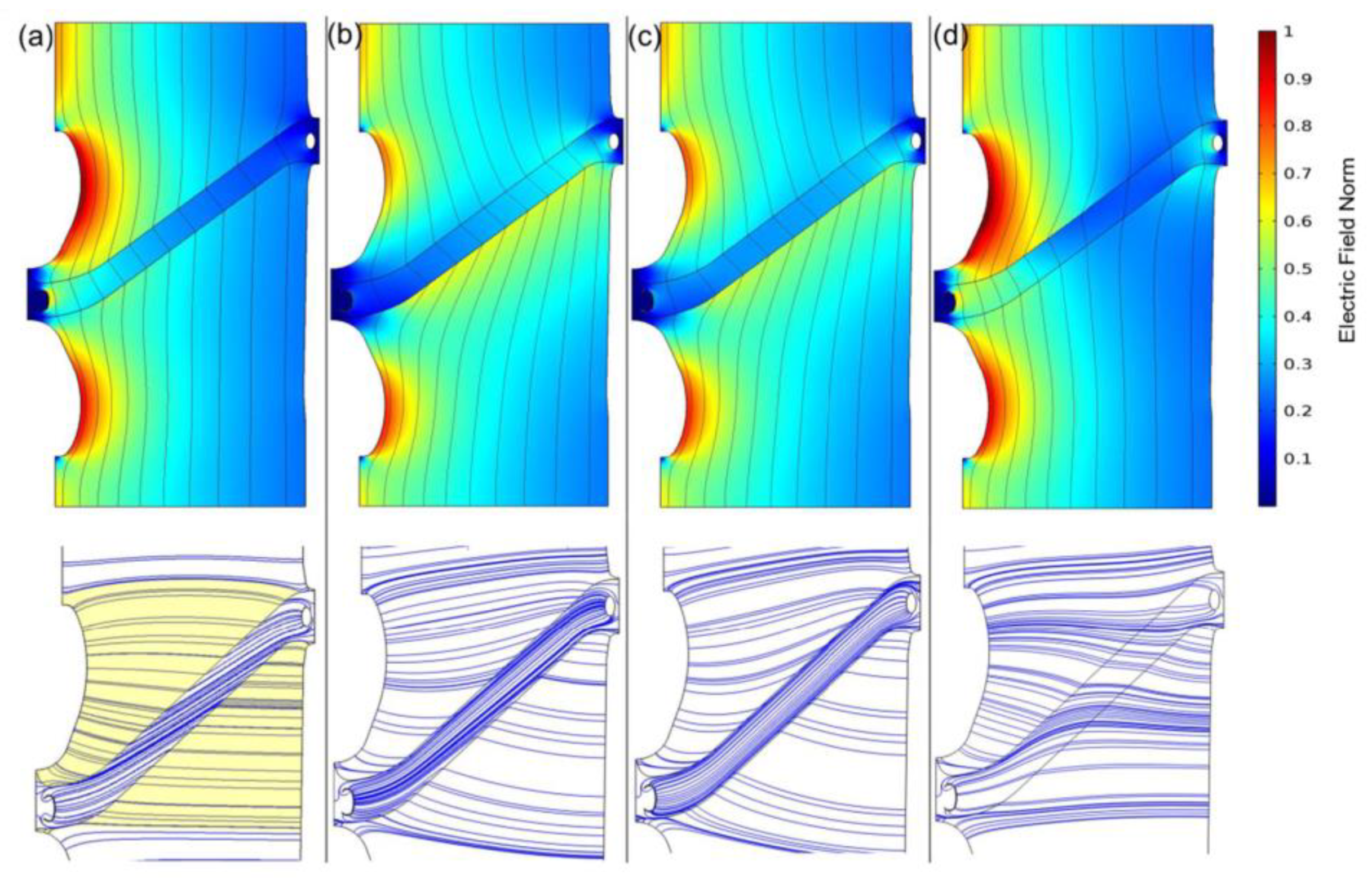
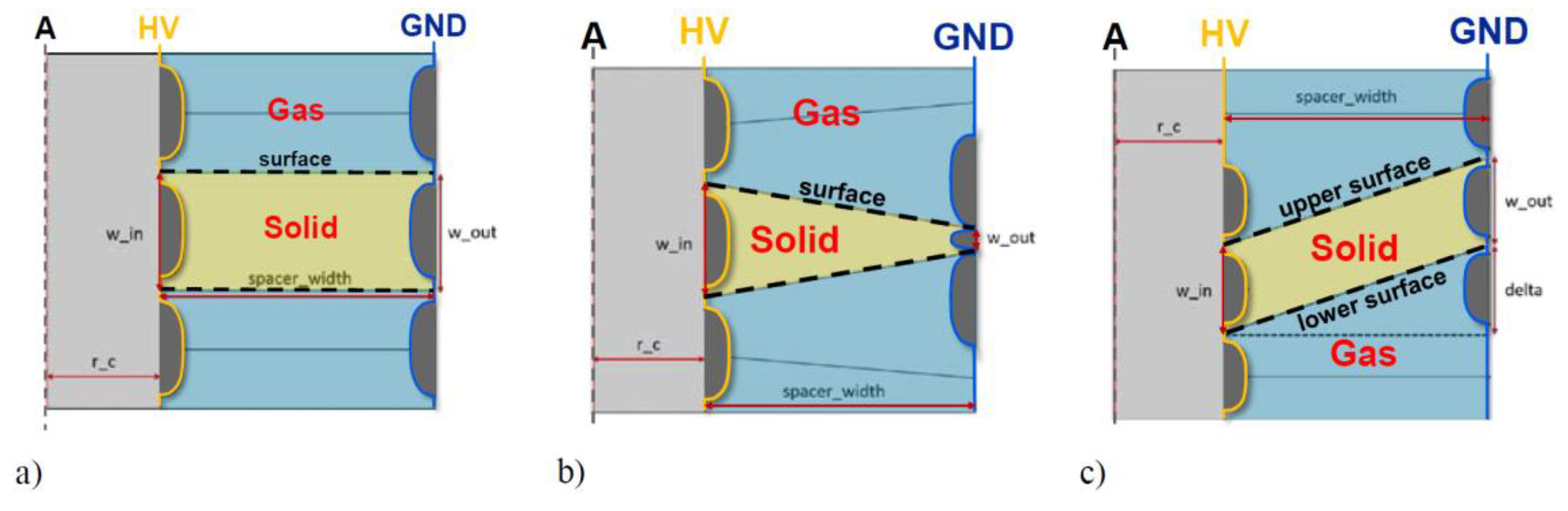
Geometrical modification of the spacer’s profile (spacer’s inclination angle, creepage distance, and thickness) can mitigate the local concentration of the electric field at the critical locations [13,38,39,40,41]. In the work [13], different spacer geometries as shown in Figure 5 have been investigated and the results were compared with an already optimized conical insulator which is commercially in DC GIS use. It has been found that the best geometry for minimizing the electric field is the rectangle version as illustrated in Figure 6, however it is not practical for mechanical and production related reasons. The second-best version is that of the already optimized conical spacer, thus confirming its reliability.
-
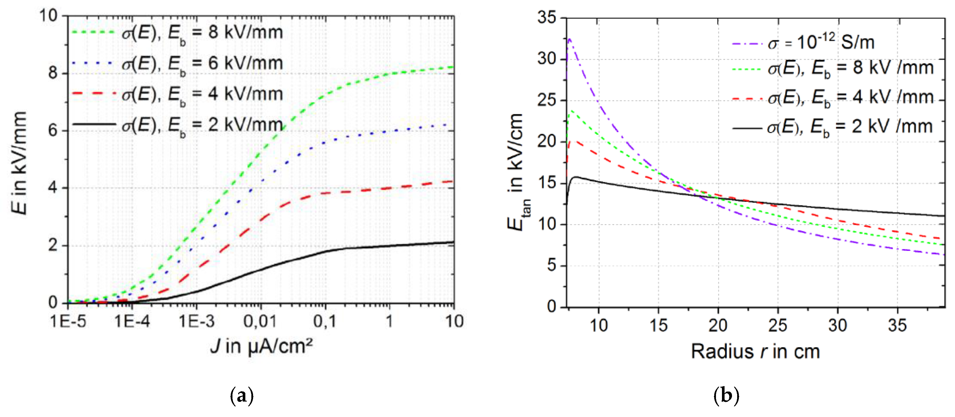
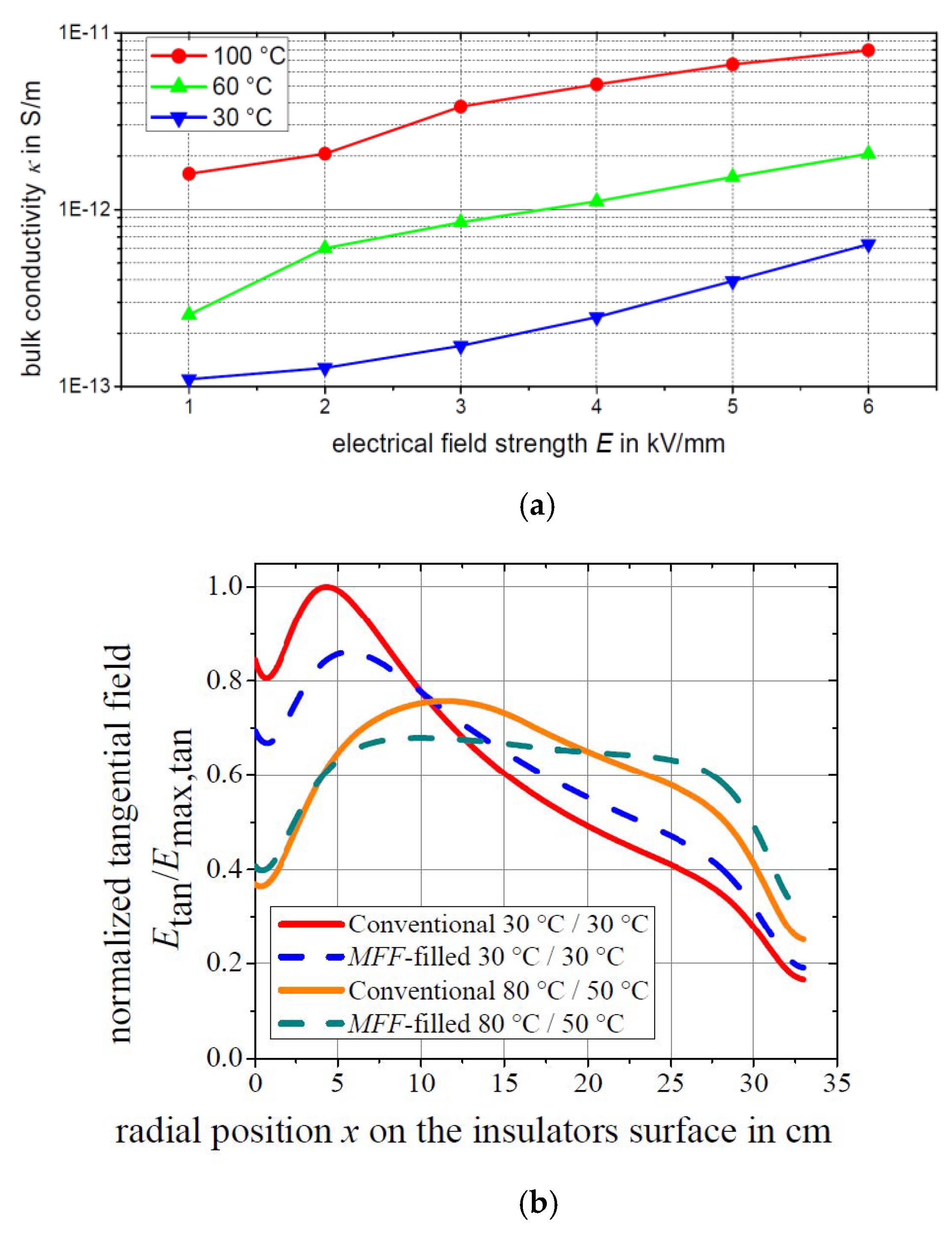
Spacers made of nonlinear conductivity electric field grading material composed of epoxy filled with a functional filler lead to a significant lowering of the electric field concentration in highly stressed regions compared to conventional epoxy spacers. Figure 7 and Figure 8 show the tangential electric field distributions under 500 kV DC along spacers made of epoxy filled with zinc oxide (ZnO) microvaristors [42] and epoxy filled with IriotecR 7000 (Merck Group Company, Darmstadt, Germany) that consist of flake shaped mica particles, covered with a nano scaled semiconducting antimony-doped tin oxide (ATO) layer, denoted in the reviewed papers as mica functional filler (MFF) [43], respectively. The experimental characteristics of the electric field dependent current density/conductivity of the two filled epoxy composites used in the simulations are also given. It should be noted that such new stress control materials are still under development.

4.2. Simulated Surface Charges’ Accumulation

The simulated charges’ accumulation on the spacer’s surface for transient and stationary conditions are obtained, as mentioned in Section 3.2, from Equations (14) and (15) respectively. The main findings on full-size conical spacers [34,37,41,43,44,46,47] can be summarized as follows:
-
In general, the accumulation of charges on the concave and convex surfaces of the conical spacer is different. Most of positive charges build up on one side of the surface while most of negative charges on the other side. In addition, the distribution of surface charges varies with the temperature distribution as reported in [44,47].
-
The accumulation of surface charges depends strongly on the conductivities of the spacer’s epoxy material and the surrounding gas. Also, if besides the natural ionization of the gas, additional ion sources are present like from electrons field emission, surface charging of the spacer is dominated by gas conduction [34,37,43].
-
The accumulated charge density on the spacer’s surface under DC steady state could be controlled by the modification of the spacer’s shape. An example is given in Figure 9 which shows that the smaller the spacer’s angle inclination (θ), the more significant surface charge density is. Moreover, it has been found that the accumulated charges can be critical when the voltage polarity is reversed [40,41].

5. Experimental Investigation

The above calculation analysis has given relevant information about the intended requirements to be met with respect to the electric field distribution around the HVDC GIS/GIL full-size epoxy spacers and surface charge accumulation under the different operating stages: DC voltage, polarity reversal, impulse voltage superimposed on DC voltage with and without temperature gradient. The main outcome is that the suitable spacers for HVDC GIL/GIS applications could be achieved by appropriate DC electric conductivity properties of the spacer’s epoxy-based material and by the optimization of its shape/geometry. To verify the validity of the obtained simulation results and to proof practically the insulation performance of the spacers, the following experimental investigations have been undertaken. Some examples of commercially available compact HVDC GIS are shown.

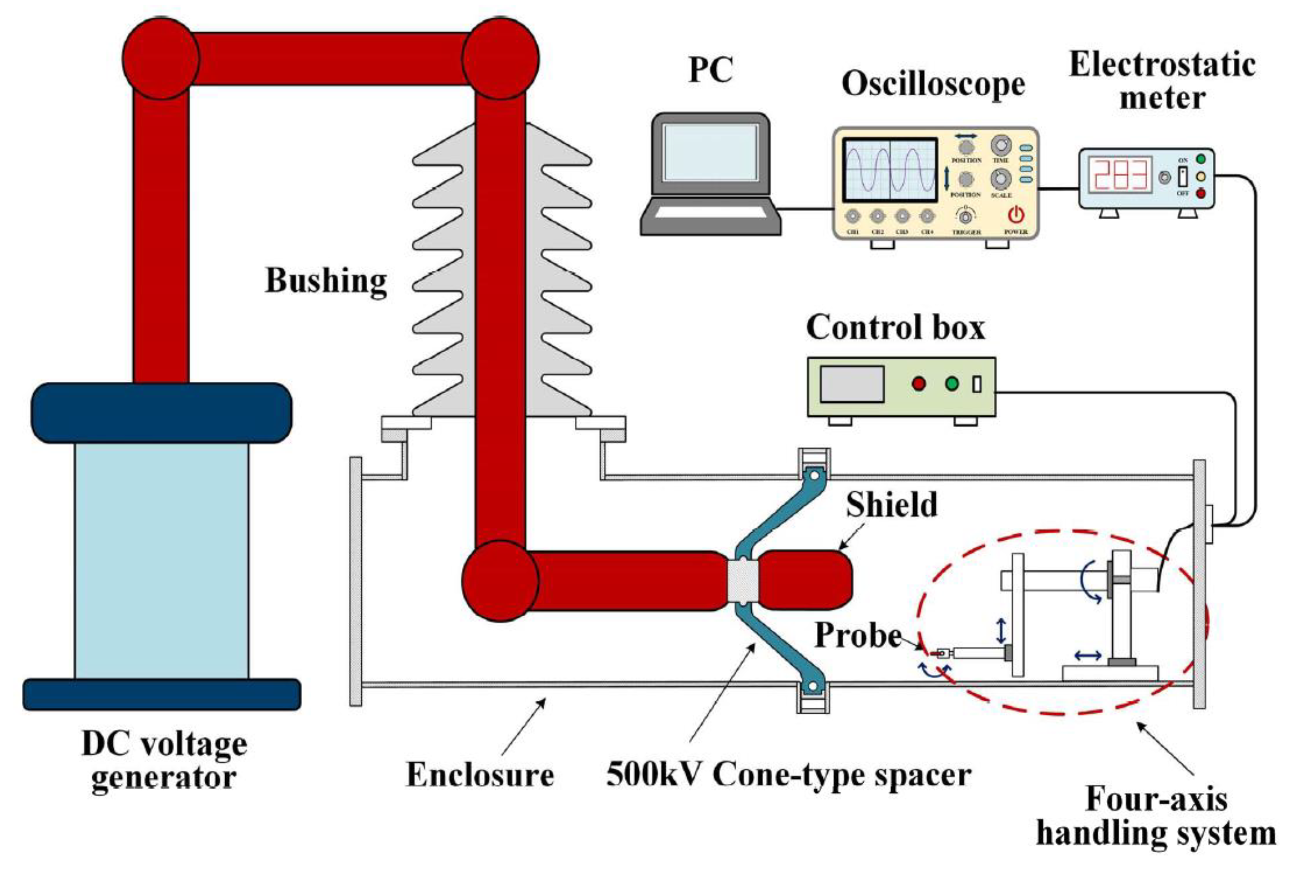
5.1. Surface Potential Measurement and Surface Charges’ Distribution

The non-contact active electrostatic probe measurement method is presently the commonly widely used test technique [48] to measure the electric potential along the spacer’s surface. This method determines the surface potential quantitatively based on the induction mechanism. The measurement is performed after the high voltage has been switched off and the electrostatic probe is placed close to the insulator surface and moved along its surface maintaining a small gap. An example of its use is illustrated by the test set-up in Figure 10 [49].
From the measured surface potential, the surface charge density distribution on the spacer is then deduced by using the charge inversion algorithm [48,50] and compared with the calculated surface charge density distribution derived from Equation 14 (transient state) or Equation (15) (steady state).
It is worth mentioning that solving the charge inversion algorithm to derive the surface charge density distribution is complex and sensitive to noise and measurements errors [48], thus the derived surface charge density is not very accurate. Therefore, another approach is considered instead where the measured surface voltage potential is directly compared to the voltage potential distribution derived from the numerically calculated surface charge density distribution, ρS, through Poisson equation: ρS = div[ε0εr(-grad V) [51].
Until now, very few works have been reported on surface charge measurements of real-size GIS/GIL spacers and the results can be summarized as follow [49,52,53,54,55,56]:
-
The build-up of surface charges is confirmed by the experimental investigations. The accumulated charge distribution depends on the DC voltage testing conditions (polarity, duration, and magnitude). The surface charge has a non-uniform distribution on the spacer, and it is highly localized in certain zones. However, the maximum surface density of the accumulated charges under the operating DC electric field is low.
-
The measured surface charge density distribution does not match the theoretical one. This difference is explained to be caused by: (i) the surface quality of the investigated spacers may present some defects caused by the casting manufacturing process, finishing, material surface morphology (size/shape of the filler and uneven distribution of the filler) that can result in further surface charge build-up; (ii) the accuracy of the surface charges measurement technique. Indeed, the measurements by the non-contact active electrostatic probe technique are done when the applied voltage is switched off and consequently some of the charges maybe neutralized or reduced especially if the measurement time is long. Moreover, and as mentioned above, solving the charge inversion algorithm to get the measured surface charge density distribution is sensitive to noise and measurement method especially for complex-shaped spacers and thus it is not very accurate.
Therefore, to study the influence of surface charges build-up, another indirect effective new method is proposed [57]. It consists of accelerating the charging of the spacer’s surface by partial discharges (PD) from an artificial sharp tip nearby the spacer (see Figure 11) prior the application of the voltages (DC, and superimposed impulse voltage on DC).

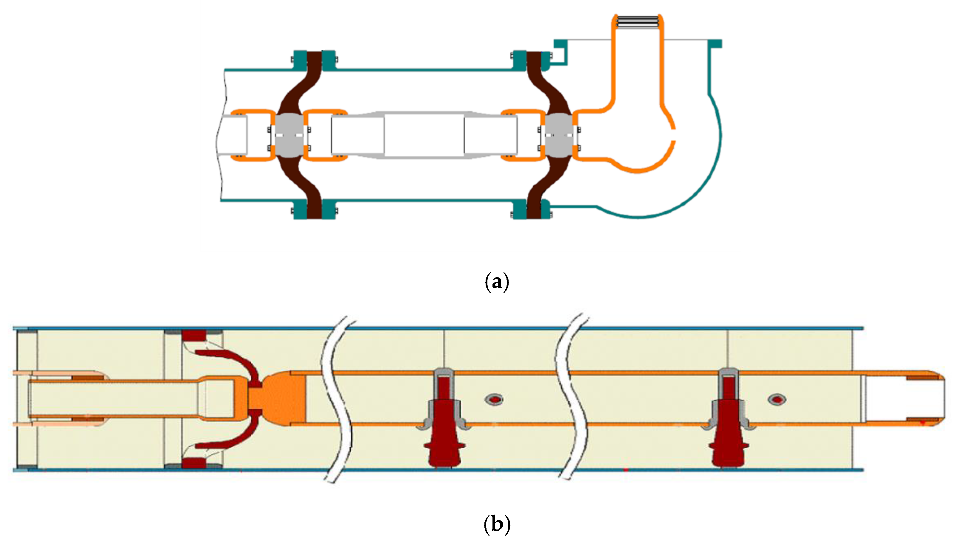
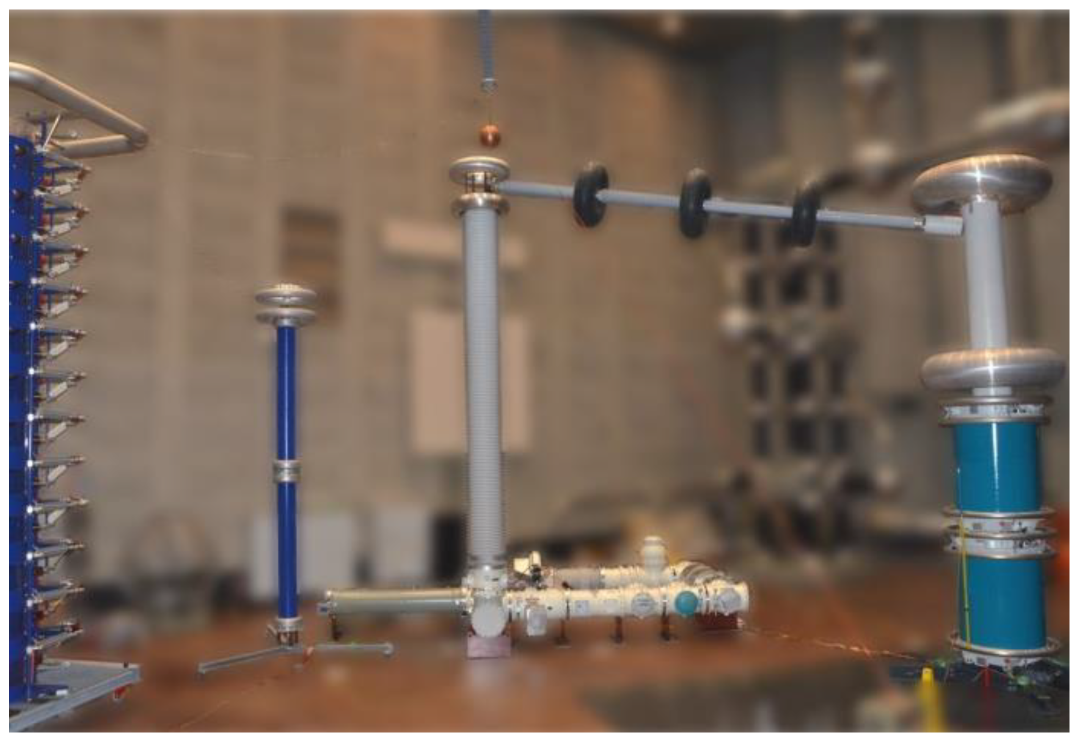
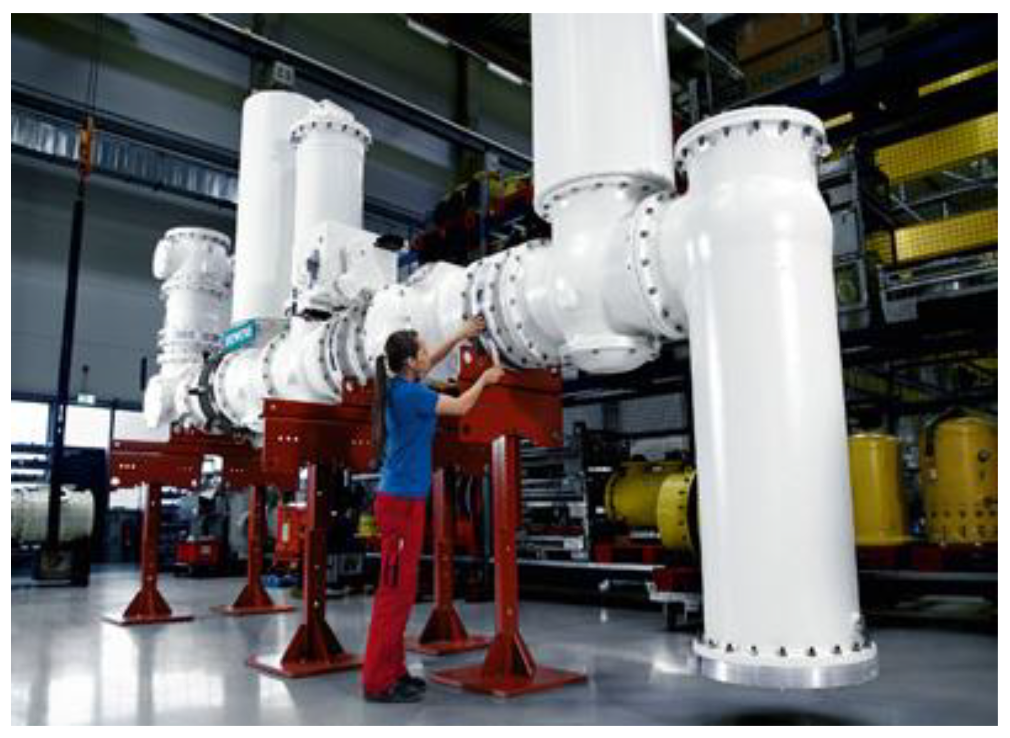
5.2. High Voltage Testing Verification and Examples of Commercially Available HVDC Gas Insulated Systems

There is currently no international DC standard for testing the insulator-gas insulation for HVDC GIS/GIL, but a draft is available based on the ongoing work of CIGRE group JWG D1/B3.57 “Dielectric testing of gas insulated HVDC systems” [58]. In general, to verify and validate the spacer-gas insulation performance, the high voltage tests are carried out using an experimental set-up represented by an electrical loop comprising several real size spacers. A current is generated in the loop to reproduce the thermal effects (high load condition) and then the different required high voltages (±DC, ±lightning/switching impulse superimposed on ±DC) tests are applied.
Up to now, only few works have been reported on the accomplished tests at production scale and they are mainly those conducted by the manufacturers Hitachi Power Grids and Siemens that led to their commercial DC gas insulated systems for ±320 kV (nominal voltage)/±350 kV (rated voltage) and ±500 kV (nominal voltage)/±550 kV (rated voltage) and those of SuperGrid Institute (Villeurbanne, France). These verification and validation tests are summarized in the following.
(1) Hitachi Power Grids
According to Hitachi Power Grids [11,13,31] and based on the electric field calculation analysis of conical type spacers for compact HVDC ±320 kV DC GIS application, a significant reduction of the electric stress was obtained by geometrical optimization of the spacers and insertion of a current collector. The verification tests were conducted successfully on a system with several insulators assembled in realistic arrangements as shown in Figure 12 by applying the tests sequence described in Table 2. The developed ±320 kV DC GIS is installed on offshore platform as illustrated in Figure 13.
Moreover, Hitachi Power Grids has provided a ±320 kV HVDC GIS prototype for long-term testing at DNV GL’s KEMA High Voltage DC Laboratory (Arnhem, The Netherlands) in the frame of the EU-funded project Progress on Meshed HVDC Offshore Transmission Networks (PROMOTioN)—Work package 15 [60]. The purpose of this prototype installation is to verify the performance of the HVDC GIS under real service conditions and to demonstrate the readiness of the technology for commercial applications. The long-term test is presently running according to the procedure given in Table 3 [61] and it is expected to finish in year 2020.
(2) Siemens
According to Siemens, the spacers that have been developed for compact HVDC for rated voltages of ±350 kV and ±550 kV GIS are conical type and those developed for ±550 kV GIL are disk type and consist of an improved epoxy composite material which fulfills the appropriate DC electric conductivity properties with respect to temperature and field dependencies and which allows a low accumulation of charges on the insulators’ surface. Extensive testing has been undertaken to validate the insulation performance of the GIS spacers for both applications. For ±350 kV and ±550 kV DC GIS, all the standard IEC 62271 dielectric tests and the DC insulation system test were passed successfully as reported in [14,15,16,20,22,62]. Figure 14 and Table 4 show the DC insulation system test set-up and the test procedure for ±550 kV DC GIS.
To investigate the ageing behavior, DC long-term performance of real-sized GIS insulators (more than 130 insulators) has been investigated under 500 kV DC voltage of both polarities where no puncture occurred for up to 40,000 testing hours [62,63]. Furthermore, results from tests on the influence of gas moisture and condensation, especially during temperature changes from −30 °C to 50 °C, have shown that higher moisture content, lead to surface flashover [64]. Thus, effective measures must be realized by the usage of drying agents as well as by thorough drying of the spacers before installation. Figure 15 shows Siemens’ first compact ±320 kV HVDC GIS [65].
Concerning the ±500 kV DC GIL [18,19,20,21,23], the insulation performance of the new insulators was verified using the same DC insulation system test set-up shown in Figure 14 and test procedure described in Table 4.
It should be noted that before commercializing the compact HVDC GIL, confirmation of its long-term capability under real service conditions and using the installation procedure as it will be used for customer projects, must be demonstrated like in the case of HVDC extruded cable systems where the prequalification’s test recommended in CIGRE technical brochure 496 [66] is usually performed. Therefore, a long-term prototype installation test for ±500 kV DC GIL has been supplied by Siemens at Griesheim Test Facility of the Technical University of Darmstadt to collect information and more experience about the reliability of HVDC GIL ±500 kV under real service conditions [67]. In this test, all the different DC GIL modules will be tested. Bending of the GIL tubes will also be applied in the test setup. In order to investigate the maximum mechanical and thermal stress, the test setup is installed as directly buried installation. The test results will be valid for tunnel and above ground installation as well since the mechanical stress is lower in these applications. The proposed preliminary test procedure is presented in [68] and it is in line with the recommendations of CIGRE working group JWG D1/B3.57. When Siemens completes these tests, the DC GIL will be approved as a reasonable alternative for reliable HVDC underground transmission solution.
(3) SuperGrid Institute
SuperGrid Institute is a French research and innovation centre which is strongly involved in the development of new insulators and gas insulation systems for DC GIS applications. It has reported in [69] that the new design of the insulators and their performance for the ±320 kV DC have been validated. The recommended tests (type test and long-term test) based on CIGRE working group JWG D1/B3.57 were conducted successfully.

6. Envisaged Research and Development of HVDC Spacers

6.1. Electric Field Control Using Advanced Field Grading Materials

Due to the environmental constraints that impose the reduction usage of the extremely potent greenhouse SF6 gas to the minimum content, a further downsizing of HVDC GIS/GIL systems with keeping high reliability is thus required. To achieve this, the optimization of downsized gas insulated systems subjected to higher applicable electric field stresses will require the application of advanced insulation techniques such as the use of electric field grading materials for lowering the local stress intensification along the spacers [70]. Two types of epoxy based materials are of interest: (i) nonlinear field dependent conductivity materials as mentioned in Section 4.1 [71] and (ii) new functionally graded materials characterized by the spatial distribution of the electric conductivity in the spacer bulk [72,73] or on the surface of the spacer [74].

6.2. Thermoplastic Polymers-Based Spacers

From the environment point of view, today’s epoxy-based spacers cannot be recycled. It appears after [75] that the thermoplastic polyethylene terephthalate (PET) is a promising alternative material to epoxy. Indeed, long term tests on real-size insulators made of commercially available PET under 400 kV AC and for more than 2 years were successful. Verification for HVDC application are to be explored.

6.3. Compatibility of the HVDC GIS/GIL Spacers with SF6-Free Alternative Gases

Since as mentioned above, SF6 is a strong greenhouse gas according to the Kyoto protocol with a high global warming potential (GWP) of approximately 23,500 over a time horizon of 100 years, the search of suitable alternative gases for HV gas insulated systems applications was in the last years of paramount importance. The environmental and safety requirements that must be fulfilled are:
-
Low GWP
-
No ozone depletion potential (ODP)
-
Low toxicity and non-flammability
-
Safe to human health
It has been found that C5-perfluoroketone (C5-PFK, NovecTM 5110, 3MTM) mixed with CO2 and O2, and C4-perfluoronitrile (C4-PFN, 3MTM NovecTM 4710) mixed with CO2, are promising gas candidates to substitute SF6 [76,77]. Indeed, at present, two types of gas mixtures have entered the market and are only in use for some commercial HVAC gas-insulated systems:
(i)
Green gas for grid (G3) [78,79] developed by GE Grid Solutions (Villeurbanne, France) in partnership with the 3M Company (Saint Paul, MN, USA) based on 4% to 6% Novec™ 4710 with CO2 which has a low GWP of 427–600, has no ozone depletion potential (ODP = 0), non-toxic, and not flammable. In addition, it is not a carcinogenic and mutagenic gas. G3 is integrated in GE Grid Solutions HVAC gas insulated products up to 420 kV [78].
(ii)
AirPlusTM gas [80,81] developed by Hitachi Power Grids in collaboration with 3M Company based on 6% NovecTM 5110 mixed with CO2 (82%) and O2(12%) which has a negligible GWP (<1), its ODP = 0, non-toxic and not flammable. It is mentioned in [81] that this gas mixture was used in a pilot GIS installation in Switzerland with a rated voltage of 170 kV.
Besides these SF6-free alternative gases, Siemens promotes the use of Clean Air (a technical air made of N2-O2) which is already in development and will be used in a 380 kV AC GIS within the framework of a German project [82].
Therefore, the compatibility and reliability of these developed environmentally-friendly gases with HVDC GIS/GIL spacers are expected to be thoroughly studied as reported for example in [83] and as planned in the EU-funded project (PROMOTioN) - Work package 15 that we mentioned in Section 5.2.

7. Conclusions

With the move to the next-generation Ultra High Voltage Direct Current (UHVDC) bulk transmission for long distances, the demand for compact HVDC GIS/GIL systems is expected to grow substantially in the coming years.
This article provides a review about full-size solid insulators (spacers) that have been so far developed for compact ±320 kV (nominal voltage)/±350 kV (rated voltage) and ±500 kV (nominal voltage)/±550 kV (rated voltage) HVDC GIS/GIL, tests qualified and commercialized. The main conclusions to be drawn from this article are the following:
-
The optimization of today’s developed spacers is based on the combination of the appropriate spacer shape design and the adjustment of the DC electric conductivity of the spacer’s epoxy material by modifying slightly its chemical composition.
-
Long term (one year) testing of HVDC GIS and GIL prototype installations have been developed to demonstrate the reliability of the systems under real service conditions.
-
Research and development activities are continuing for higher electric field applications where new advanced insulation techniques such as electric field grading materials and functionally graded materials will be required to be integrated.
-
Furthermore, as the developed gases C5-perfluoroketone mixed with CO2 and O2, and C4-perfluoronitile mixed with CO2 have entered the market and are presently used as alternative to SF6 in some commercial HVAC gas insulated systems, their reliability and compatibility with the epoxy insulators of the HVDC GIS/GIL will be in the future extensively studied and test verified.

Author Contributions

Conceptualization, N.Z.; validation, M.A.H.; investigation, N.Z.; writing—original draft preparation, N.Z.; writing—review and editing, M.A.H.; visualization, N.Z. All authors have read and agreed to the published version of the manuscript.

Funding

This work received no external funding.

Acknowledgments

The authors would like to thank warmly Hermann Koch (www.drkochconsulting.com) worldwide known expert in the field of both HVAC and HVDC GIS/GIL (several books and publications), for the technical comments and feedback for the preparation of this review paper.

Conflicts of Interest

The authors declare no conflict of interest.

References

  1. NKT A/S. World´s Most Powerful Underground Power Transmission Cable System. Available online: https://www.nkt.com/products-solutions/high-voltage-cable-solutions/innovation/640-kv-extruded-hvdc-cable-systems (accessed on 24 October 2019).
  2. Nitta, T.; Nakanishi, K. Charge Accumulation on Insulating Spacers for HVDC GIS. IEEE Trans. Dielectr. Electr. Insul. 1991, 26, 418–427. [Google Scholar] [CrossRef]
  3. Hasegawa, T.; Yamaji, K.; Hatano, M.; Endo, F.; Aoyagi, H.; Taniguchi, Y.; Kobayashi, A. DC Dielectric Characteristics and Conception of Insulation Design for DC GIS. IEEE Trans. Power Deliv. 1996, 11, 1776–1782. [Google Scholar] [CrossRef]
  4. Hasegawa, T.; Yamaji, K.; Hatano, M.; Endo, F.; Rokunohe, T.; Yamagiwa, T. Development of Insulation Structure and Enhancement of Insulation Reliability of 500 kV DC GIS. IEEE Trans. Power Deliv. 1997, 12, 194–202. [Google Scholar] [CrossRef]
  5. Shikata, M.; Yamaji, K.; Hatano, M. Development and design of DC GIS. Electr. Eng. Jpn. 1999, 129, 51–61. [Google Scholar] [CrossRef]
  6. Shimato, T.; Hashimoto, T.; Sampei, M. The Kii Channel HVDC Link in Japan; CIGRE: Paris, France, 2002. [Google Scholar]
  7. Yasuoka, T.; Abe, Y.; Shiiki, M.; Karube, T. Dielectric Tests for 250 kV DC-GIS. In Proceedings of the CIGRE-IEC 2019 Conference on EHV and UHV (AC&DC), Hakodate, Hokkaido, Japan, 23–26 April 2019. [Google Scholar]
  8. Yasuoka, T.; Hoshina, Y.; Shiiki, M.; Takei, M.; Kumada, A.; Hikada, K. Insulation characteristics in DC-GIS: Surface charge phenomena on epoxy spacer and metallic particle motions. In Proceedings of the CIGRE Conference, Paris, France, 26–31 August 2018. [Google Scholar]
  9. Shigemitsu, O.; Genyo, U.; Tomoaki, U.; Jun, N. Insulation Characteristics of GIS Insulators under Lightning Impulse with DC Voltage Superimposed. IEEE Trans. Dielectr. Electr. Insul. 2015, 22, 3269–3277. [Google Scholar]
  10. Shigemitsu, O.; Genyo, U.; Kenichi, N. Insulation Characteristics of GIS Epoxy Insulators with Non-uniform Surface Resistance under DC Voltage. IEEE Trans. Dielectr. Electr. Insul. 2015, 22, 516–525. [Google Scholar]
  11. Riechert, U.; Gremaud, R.; Thorson, S.; Callavik, M. Application options and electrical field studies as basis for adequate testing of gas-insulated systems for HVDC. In Proceedings of the CIGRE Winnipeg 2017 Colloquium Study Committees A3, B4 & D1, Winnipeg, MB, Canada, 30 September–6 October 2017. [Google Scholar]
  12. Gremaud, R.; Riechert, U.; Straumann, U. Compact Gas-insulated Systems for High Voltage Direct Current Transmission: Basic Design. In Proceedings of the 2016 IEEE PES Transmission & Distribution Conference & Exposition, Dallas, TX, USA, 3–5 May 2016. [Google Scholar]
  13. Riechert, U.; Straumann, U.; Gremaud, R.; Callavik, M. Compact Gas-insulated Systems for High Voltage Direct Current Transmission: Design and Testing. In Proceedings of the 2016 IEEE PES Transmission & Distribution Conference & Exposition, Dallas, TX, USA, 3–5 May 2016. [Google Scholar]
  14. Hering, M.; Koch, H.; Jurhe, K. Direct Current High-Voltage Gas Insulated Switchgear up to ±550 kV. In Proceedings of the CIGRE-IEC 2019 Conference on EHV and UHV (AC&DC), Hakodate, Hokkaido, Japan, 23–26 April 2019. [Google Scholar]
  15. Tenzer, M.; Koch, H.; Imamovic, D. Compact Systems for High Voltage Direct Current Transmission. In Proceedings of the International ETG Congress, Bonn, Germany, 17–18 November 2015. [Google Scholar]
  16. Imamovic, D.; Lutz, B.; Juhre, K.; Uecker, K.; Langens, A. Development of 320 kV DC Compact Switchgear; CIGRE: Toronto, ON, Canada, 2014. [Google Scholar]
  17. Siemens Energy. Gas-insulated DC Switchgear (DC GIS). Available online: https://www.siemens-energy.com/global/en/offerings/power-transmission/transmission-products/gas-insulated/dc-gis.html (accessed on 24 October 2020).
  18. Magier, T.; Tenzer, M.; Koch, H. Direct Current Gas-Insulated Transmission Lines. IEEE Trans. Power Deliv. 2018, 33, 440–446. [Google Scholar] [CrossRef]
  19. Tenzer, M.; Rudenko, P.; Koch, H. Direct Current Gas-Insulated Transmission Lines: Development and testing of the ±550 kV DC GIL. In Proceedings of the International Symposium on HVDC Cable Systems, Dunkirk, France, 20–22 November 2017. [Google Scholar]
  20. Koch, H.; Imamovic, D.; Lutz, B.; Juhre, K.; Neidhart, T.; Rogler, R.D. High Power Underground Transmission for HVDC. In Proceedings of the CIGRE Conference, Paris, France, 22–26 August 2016. paper B3-104. [Google Scholar]
  21. Tenzer, M.; Koch, H.; Imamovic, D. Underground transmission lines for AC and DC. In Proceedings of the 2016 IEEE/PES Transmission and Distribution Conference and Exposition (T&D), Texas, USA, 3–5 May 2016. [Google Scholar]
  22. Koch, H.; Imamovic, D. High Power AC and DC Underground Transmission Lines. In Proceedings of the 2016 CIGRE-IEC Colloquium, Montreal, QC, Canada, 9–11 May 2016. [Google Scholar]
  23. Imamovic, D.; Tenzer, M.; Koch, H. High Power Underground Transmission Lines. In Proceedings of the 9th International Conference on Insulated Power Cables-Jicable 2015, Versailles, France, 21–25 June 2015. [Google Scholar]
  24. Li, C.; Lin, C.; Yang, Y.; Zhang, B.; Liu, W.; Li, Q.; Hu, J.; He, S.; Liu, X.; He, J. Novel HVDC Spacers by Adaptively Controlling Surface Charges—Part I: Charge Transport and Control Strategy. IEEE Trans. Dielectr. Electr. Insul. 2018, 25, 1238–1247. [Google Scholar]
  25. Li, C.; Lin, C.; Yang, Y.; Zhang, B.; Liu, W.; Li, Q.; Hu, J.; He, S.; Liu, X.; He, J. Novel HVDC Spacers by Adaptively Controlling Surface Charges—Part II: Experiment. IEEE Trans. Dielectr. Electr. Insul. 2018, 25, 1248–1258. [Google Scholar]
  26. Li, C.; Lin, C.; Yang, Y.; Zhang, B.; Liu, W.; Li, Q.; Hu, J.; He, S.; Liu, X.; He, J. Novel HVDC Spacers by Adaptively Controlling Surface Charges—Part III: Industrialization Prospects. IEEE Trans. Dielectr. Electr. Insul. 2018, 25, 1259–1266. [Google Scholar]
  27. Hering, M.; Gremaud, R.; Speck, J.; Groβmann, S.; Riechert, U. Flashover behaviour of insulators with inhomogeneous temperature distribution in gas insulated systems under DC voltage stress. In Proceedings of the 2014 ICHVE International Conference on High Voltage Engineering and Application, Boznan, Poland, 8–11 September 2014. [Google Scholar]
  28. Zebouchi, N.; Li, H.; Haddad, M. Development of Future Compact and Eco-Friendly HVDC Gas-Insulated Systems: Shape Optimization of a DC Spacer Model and Novel Materials Investigation. Energies 2020, 13, 3288. [Google Scholar] [CrossRef]
  29. Li, C.; Liu, B.; Wang, J.; Gong, R.; Wang, G.; Lei, Z.; Fabiani, D.; Lin, C.; Hu, J. Novel HVDC Spacers in GIS/GIL by Adaptively Controlling Surface Charges—Insulation Compounding Scheme. In Proceedings of the 2nd International Conference on High Voltage Engineerin and Power Systems (ICHVEPS), Bali, Indonesia, 1 October 2019. [Google Scholar]
  30. Koch, H.; Hopkins, M. Overview of Gas Insulated Lines (GIL). In Proceedings of the IEEE Power Engineering Society General Meeting, San Francisco, CA, USA, 16 June 2005; pp. 940–944. [Google Scholar]
  31. Riechert, U.; Blumenroth, F.; Straumann, U.; Kaufmann, B.; Saltzer, M.; Bergelin, P. Experiences in Dielectric Testing of Gas-insulated HVDC Systems. In Proceedings of the CIGRE Conference, Paris, France, 26–31 August 2018. [Google Scholar]
  32. Endo, F.; Hama, H.; Okabe, S.; Juhre, K.; Kindersberger, J.; Meijer, S.; Schichler, U. Gas Insulated System for HVDC: DC Stress at DC and AC Systems; CIGRE Technical Brochure 506; CIGRE: Paris, France, 2012; ISBN 978-2-85873-198-5. [Google Scholar]
  33. Imamovic, D. Compact Systems for HVDC Applications. In Proceedings of the Symposium Energieinnovation, Graz, Austria, 12–14 February 2014. [Google Scholar]
  34. Gremaud, R.; Molitor, F.; Doiron, C.; Christen, T.; Riechert, U.; Straumann, U.; Kallstrand, B.; Johansson, K.; Hjorstram, O. Solid Insulation in DC Gas-Insulated Systems. In Proceedings of the CIGRE Conference, Paris, France, 24–29 August 2014. [Google Scholar]
  35. Vu-Cong, T.; Zavattoni, L.; Vinson, P.; Girodet, A. DC GIS: Importance of Simulations for the Design and Testing; CIGRE D1-102; CIGRE: Paris, France, 2016. [Google Scholar]
  36. Vu-Cong, T.; Vinson, P.; Girodet, A. Simulation Methodology for DC GIS. In Proceedings of the MATPOST 2015, 5th International Substation Equipment’s Conference, Lyon, France, 24 November 2015. [Google Scholar]
  37. Winter, A.; Kindersberger, J. Transient Field Distribution in Gas-Solid Insulation Systems under DC Voltages. IEEE Trans. Dielectr. Electr. Insul. 2014, 21, 116–128. [Google Scholar] [CrossRef]
  38. Hong Koo, J.; Hwang, J.-S.; Kwon, I.-S.; Lee, H.-Y.; Ju Shin, W.; Lee, B.-W. Modeling and simulation of HVDC epoxy spacer for SF6 gas insulated system. In Proceedings of the 19th International Symposium on High Voltage Engineering, Pilsen, Czech Republic, 23–28 August 2015. [Google Scholar]
  39. Sakai, T.; Furuyashiki, T.; Kato, K.; Okubo, H. Electric field analysis and electrical insulation performance for solid insulator in HVDC gas insulated switchgear. In Proceedings of the 19th International Symposium on High Voltage Engineering, Pilsen, Czech Republic, 23–28 August 2015. [Google Scholar]
  40. Nakane, R.; Takabayashi1, K.; Kato, K.; Okubo, H. Electric field analysis an electrical insulation performance for Gas-Solid composite insulation in HVDC GIS. In Proceedings of the 20th International Symposium on High Voltage Engineering, Buenos Aires, Argentina, 27 August–1 September 2017. [Google Scholar]
  41. Nakane, R.; Takabayashi1, K.; Kato, K.; Okubo, H. Electrical insulation performance of HVDC-GIS spacer under various testing conditions. In Proceedings of the IEEE Conference on Electrical Insulation and Dielectric Phenomena, Fort Worth, TX, USA, 22–25 October 2017. [Google Scholar]
  42. Tenzer, M.; Hinrichsen, H. Investigations on microvaristor-filled polymeric insulating materials focused on DC applications. In Proceedings of the 22nd Nordic Insulation Symposium, NORD-IS 11, Tampere, Finland, 13–15 June 2011. [Google Scholar]
  43. Winter, A.; Kindersberger, J.; Tenzer, M.; Hinrichsen, V.; Zavattoni, L.; Lesaint, O.; Muhr, M.; Imamovic, D. Solid/Gaseous insulation systems for compact HVDC solutions. In Proceedings of the CIGRE Conference, Paris, France, 24–29 August 2014. [Google Scholar]
  44. Du, B.X.; Liang, H.C.; Li, J.; Ran, Z.Y. Electrical Field Distribution along SF6/N2 Filled DC-GIS/GIL Epoxy Spacer. IEEE Trans. Dielectr. Electr. Insul. 2018, 25, 1203–1210. [Google Scholar] [CrossRef]
  45. Vu-Cong, T.; Jacquier, F.; Girodet, A. Electric field computation for HVDC GIS/GIL spacer under superimposed impulse conditions. In Proceedings of the 2019 IEEE Conference on Electrical Insulation and Dielectric Phenomena, Richland, WA, USA, 20–23 October 2019. [Google Scholar]
  46. Zhang, B.; Guo, Y.; Yao, Y.; Wang, Z.; Zhang, H.; Jin, G. Charge transport and accumulation around the cone-type insulator in SF6-filled 550 kV DC GIL. J. Eng. 2019, 2019, 2610–2614. [Google Scholar] [CrossRef]
  47. Hong-Yang, Z.; Guo-Ming, M.; Cheng-Rong, L.; Cheng, S.; Si-Chen, Q. Impact of temperature on surface charges accumulation on insulators in SF6-filled DC GIL. IEEE Trans. Dielectr. Electr. Insul. 2017, 24, 601–610. [Google Scholar]
  48. Zhang, L.; Lin, C.; Li, C.; Suraci, S.V.; Chen, G.; Riechert, U.; Shahsavarian, T.; Hikita, M.; Tu, Y.; Zhang, Z.; et al. Gas–solid interface charge characterisation techniques for HVDC GIS/GIL insulators. High Volt. 2020, 5, 95–109. [Google Scholar] [CrossRef]
  49. Zhou, H.; Ma, G.; Wang, Y.; Li, C.; Tu, Y.; Ye, S.; Zhang, B.; Guo, X.; Yan, X. Surface Charge Accumulation on 500kV Cone-Type GIS Spacer under Residual DC Voltage. IEEE Trans. Dielectr. Electr. Insul. 2018, 25, 1230–1237. [Google Scholar] [CrossRef]
  50. Chuanjie, L.; Chuanyang, L.; Jinliang, H.; Jun, H.; Bo, Z. Surface Charge Inversion Algorithm Based on Bilateral Surface Potential Measurements of Cone-type Spacer. IEEE Trans. Dielectr. Electr. Insul. 2017, 24, 1905–1912. [Google Scholar]
  51. Gremaud, R.; Doiron, C.B.; Baur, M.; Simka, P.; Teppati, V.; Källstrand, B.; Johansson, K.; Hering, M.; Speck, J.; Großmann, S.; et al. Solid-gas insulation in HVDC gas-insulated system: Measurement, modeling and experimental validation for reliable operation. CIGRE Sci. Eng. 2017, 7, 133–142. [Google Scholar]
  52. Zhao, S.; Kindersberger, J.; Hering, M.; Juhre, K. Measurement of surface potential at the gas-solid interface for validating electric field simulations in gas-insulated DC systems. In Proceedings of the CIGRE Conference, Paris, France, 26–31 August 2018. [Google Scholar]
  53. Vu-Cong, T.; Zavattoni, L.; Vinson, P.; Girodet, A. Surface charge measurements on epoxy spacer in HVDC GIS/GIL in SF6. In Proceedings of the IEEE Conference on Electrical Insulation and Dielectric Phenomena, Toronto, ON, Canada, 16–19 October 2016. [Google Scholar]
  54. Zhang, B.Y.; Wang, Q.; Zhang, G.X. Measurement and modeling of surface charge accumulation on insulators in HVDC gas insulated line (GIL). CIGRE Sci. Eng. 2015, 3, 81–88. [Google Scholar]
  55. Qiang, W.; Guixin, Z.; Xinxin, W. Characteristics and Mechanisms of Surface Charge Accumulation on a Cone-type Insulator under dc Voltage. IEEE Trans. Dielectr. Electr. Insul. 2012, 19, 150–155. [Google Scholar] [CrossRef]
  56. Wang, Q.; Zhang, G.X.; Wang, X.X.; Wang, B. Surface Charge Accumulation on the Cone-Type Insulator under DC Voltage. In Proceedings of the IEEE International Power Modulator and High Voltage Conference, Atlanta, GA, USA, 23–27 May 2010. [Google Scholar]
  57. Juhre, K.; Lutz, B.; Imamovic, D. Testing and long-term performance of gas-insulated DC compact switchgear. CIGRE Sci. Eng. 2016, 6, 103–108. [Google Scholar]
  58. CIGRE Working Group. JWG D1/B3.57 “Dielectric Testing of Gas Insulated HVDC Systems”; Draft Paper; CIGRE: Paris, France, 2013. [Google Scholar]
  59. ABB. ABB Installs Latest HVDC Gas-Insulated Switchgear Innovation. Available online: https://new.abb.com/news/detail/7703/abb-installs-latest-hvdc-gas-insulated-switchgear-innovation (accessed on 24 October 2019).
  60. Transformers Magazine. DNV GL Completes HVDC GIS Test Prototype Installation. Available online: https://transformers-magazine.com/tm-news/5900-dnv-gl-completes-hvdc-gis-test-prototype-installation/ (accessed on 24 October 2019).
  61. Sperling, E.; Riechert, U. Long-term qualification procedure on a GIS HVDC RC-divider and HVDC GIS system up to ±350 kV. In Proceedings of the CIGRE-IEC 2019 Conference on EHV and UHV (AC&DC), Hakodate, Hokkaido, Japan, 23–26 April 2019. [Google Scholar]
  62. Juhre, K.; Hering, M. Testing and long-term performance of gas-insulated systems for DC application. In Proceedings of the CIGRE-IEC 2019 Conference on EHV and UHV (AC&DC), Hakodate, Hokkaido, Japan, 23–26 April 2019. [Google Scholar]
  63. Lutz, B.; Juhre, K.D. Imamovic. Long-term term performance of solid insulators in gas insulated systems under HVDC stress. In Proceedings of the 19th International Symposium on High Voltage Engineering, Pilsen, Czech Republic, 23–28 August 2015.
  64. Juhre, K.; Hering, M. Influence of extreme temperature conditions on the gas-solid insulating system under DC voltage stress. In Proceedings of the CIGRE Winnipeg 2017 Colloquium Study Committees A3, B4 & D1, Winnipeg, MB, Canada, 30 September–6 October 2017. [Google Scholar]
  65. Siemens. Gas Insulated DC Switchgear for up to ±550 kV, 5000 A; Siemens DC GIS Technical Brochure; Siemens AG: Erlangen, Germany, 2013; Available online: https://assets.new.siemens.com/siemens/assets/api/uuid:eaee0c6a63a0f7edf5372a1f5a370fefd53de9ab/e50001-g630-a240-x-4a00-ws-gis-8dq1-1-550-kv-lowres.pdf (accessed on 24 October 2020).
  66. CIGRE. Recommendations for Testing DC Extruded Cable Systems for Power Transmission at a Rated Voltage up to 500 kV; CIGRE Technical Brochure 496; CIGRE: Paris, France, 2012. [Google Scholar]
  67. Available online: https://www.hst.tu-darmstadt.de/links_2/projekt__griesheim_/inhalt_mit_marginalienspalte_184.de.jsp (accessed on 24 October 2019).
  68. Neumann, C.; Hallas, M.; Felk, M.; Tenzer, M.; Riechert, U. Some thoughts regarding prototype installation tests of gas-insulated HVDC systems. In Proceedings of the CIGRE Winnipeg 2017 Colloquium Study Committees A3, B4 & D1, Winnipeg, MB, Canada, 30 September–6 October 2017. [Google Scholar]
  69. Vu-Cong, T.; Ortiz, G.; Jacquier, F.; Vinson, P.; Girodet, A. Design and validation tests of 320 kV HVDC GIL/GIS. In Proceedings of the MATPOST 2019 Conference, Lyon, France, 20–22 November 2019. [Google Scholar]
  70. CIGRE. Optimized Gas-Insulated Systems by Advanced Insulation Techniques; CIGRE Technical Brochure 571; CIGRE: Paris, France, 2014. [Google Scholar]
  71. Hering, M.; Juhre, K.; Secklehner, M.; Hinrichsen, V. Requirements on Solid Insulating Materials and Gas-Solid Interfaces in Compact HVDC Gas-Insulated Systems. In Proceedings of the 20th International Symposium on High Voltage Engineering, Buenos Aires, Argentina, 27 August–1 September 2017. [Google Scholar]
  72. Hayakawa, N.; Oishi, R.; Kojima, H.; Zebouchi, N. Electric Field Grading by Functionally Graded Materials (FGM) for HVDC Gas Insulated Power Apparatus. In Proceedings of the IEEE Conference on Electrical Insulation and Dielectric Phenomena, Cancun, Mexico, 21–24 October 2018. [Google Scholar]
  73. Rachmawati, I.A.; Nakane, R.; Kojima, H.; Kato, K.; Zebouchi, N.; Hayakawa, N. Electric Field Grading by Permittivity and Conductivity Graded Materials (ε/σ-FGM) for HVDC Gas Insulated Power Apparatus. In Proceedings of the 2020 International Symposium on Electrical Insulating Materials (ISEIM 2020), Tokyo, Japan, 13–17 September 2020. [Google Scholar]
  74. Li, J.; Liang, H.C.; Du, B.X.; Wang, Z.H. Surface Functional Graded Spacer for Compact HVDC Gaseous Insulated System. IEEE Trans. Dielectr. Electr. Insul. 2019, 26, 664–667. [Google Scholar] [CrossRef]
  75. Juhre, K.; Siemens, Berlin, Germany. Private communication, 2012.
  76. Seeger, M.; Smeets, R.; Yan, J.; Ito, H.; Claessens, M.; Dullni, E.; Franck, C.M.; Gentils, F.; Hartmann, H.; Kiefel, Y.; et al. Recent development of alternative gases to SF6 for switching applications. Electra 2017, 291, 26–29. [Google Scholar]
  77. Li, X.; Zhao, H.; Murphy, A.-B. SF6-alternative gases for application in gas-Insulated switchgear. J. Phys. D Appl. Phys. 2018, 51, 153001. [Google Scholar] [CrossRef]
  78. General Electric. g3—SF6 Alternative For High Voltage Applications. Available online: https://www.gegridsolutions.com/HVMV_Equipment/catalog/g3/ (accessed on 24 October 2020).
  79. Baofeng, P.; Guoming, W.; Huimin, S.; Jiahua, S.; Hong-Keun, J.; Gyung-Suk, K. Green Gas for Grid as an Eco-Friendly Alternative Insulation Gas to SF6: A Review. MDPA Appl. Sci. 2020, 10, 2526. [Google Scholar]
  80. ABB. AirPlusTM: An Alternative to SF6 as an Insulation and Switching Medium in Electrical Switchgear. Available online: https://library.e.abb.com/public/3405a31190934a8c98997eca8fc811be/ABB%20Review%202-2016_AirPlus_An%20Alternative%20to%20SF6.pdf (accessed on 24 October 2020).
  81. Diggelmann, T.; Tehlar, D.; Müller, P. 170 kV Pilot Installation with a Ketone Based Insulation Gas with First Experience from Operation in the Grid. CIGRE Conference: Paris, France, 2016; pp. 105–113. [Google Scholar]
  82. Siemens Energy. Siemens to Retrofit One of the Largest Substations in Germany. Available online: https://press.siemens.com/global/en/pressrelease/siemens-retrofit-one-largest-substations-germany (accessed on 24 October 2019).
  83. Wang, C.; Cheng, Y.; Tu, Y.; Chen, G.; Yuan, Z.; Xiao, A.; Owens, J.; Zhang, A.; Mi, N. Characteristics of C3F7CN/CO2 as an Alternative to SF6 in HVDC-GIL Systems. IEEE Trans. Dielectr. Electr. Insul. 2018, 25, 1351–1356. [Google Scholar] [CrossRef]
Figure 1. Type of insulators. (a) Gas-tight conical insulators of a GIS busbar section (dark brown). (b) Post-type and non-gas tight conical insulators (brown) of a straight welded construction of GIL [30].
Energies 13 06416 g001
Figure 2. Relevant physical mechanisms occurring in the insulation of DC GIS/GIL systems [33].
Energies 13 06416 g002
Figure 3. Electric field for conical insulator. Top: Field distribution and equipotential lines for a conical insulator; Bottom: Field lines (yellow filled area: ion capture volume) at 330 kV for (a) capacitive, (b) DC, 10−21 S/m residual gas conductivity, 0 IP/(cm3·s), (c) DC, 29 IP/(cm3·s) (ions from natural ionization), (d) DC, 290 IP/(cm3·s) (10 × natural ionization). 20° K temperature gradient on insulator surface [34].
Energies 13 06416 g003
Figure 4. Electric field distribution along the conical spacer under DC voltage. (a) Without temperature gradient and (b) with temperature gradient ΔT between the conductor and the enclosure [20].
Energies 13 06416 g004
Figure 5. Geometries of (a) rectangular, (b) trapezoidal, (c) slanted insulators. HV conductor radius = 50 mm, spacer width = 120 mm, spacer thickness = 50 mm (a,c) [13].
Energies 13 06416 g005
Figure 6. Resistive and capacitive electric field along the solid-gas interface for all considered geometries. The applied voltage is 100 kV [13].
Energies 13 06416 g006
Figure 7. Graphs of the electric conductivity of ZnO microvaristor filled epoxy and the resulting electric field distribution along the insulator’s surface. (a) Nonlinear E-J curves. (b) Distribution of the tangential electric field Etang along the insulator surface under 500 kV DC in comparison with that of σ = 10−12 S/m [42].
Energies 13 06416 g007
Figure 8. Graphs of the electric conductivity of MFF filled epoxy and the resulting electric field distribution along the insulator’s surface. (a) Measured bulk conductivity at three different temperatures (30 °C, 60 °C and 100 °C). (b) Normalized tangential electric field distribution Etang at the insulator’s surface made of MFF filled epoxy under 500 kV DC for constant temperature (30 °C) and gradient temperature compared to conventional epoxy material σ (30 °C) = 10−13 S/m [43].
Energies 13 06416 g008
Figure 9. Epoxy spacer configuration and charge density distribution along the spacer surface under 500 kV DC while changing the inclination angle of the spacer (thickness = 30 mm, σspacergas = 0.1) [40].
Energies 13 06416 g009
Figure 10. Schematic drawing of the experimental system setup [49].
Energies 13 06416 g010
Figure 11. Illustrative exemple of (a) apparatus to charge insulators by partial discharges (PD) at an automatically moveable tip and (b) space charge distribution generated by PD from a sharp tip [57].
Energies 13 06416 g011
Figure 12. Tests’ verification of the spacers’ insulation performance. (a) Test set-up and (b) test loop comprising several insulators [11].
Energies 13 06416 g012
Figure 13. Hitachi Power Grids installation of compact ±320 kV HVDC GIS on offshore platform in the North Sea [59].
Energies 13 06416 g013
Figure 14. Test setup of an insulation system test [62].
Energies 13 06416 g014
Figure 15. Siemens’ first compact ±320 kV HVDC GIS [65].
Energies 13 06416 g015
Table 1. Electric conductivity models considered for the electric field calculation.
Insulation DomainElectric Conductivity Model
Spacer
σ = constant
σ = σ (E) = σ0eαE
α (m/V) is the electric field dependency coefficient
σ = σ (E,T) = σ0eαE eβT
β (1/K) is the temperature dependency coefficient
σ = σ (E,T) = σ0eαE e−W/kBT
T (K) is the temperature; kB is Boltzmann constant (J/K) and W (J) is the thermal activation energy
σ = σ (E) = σ0 (E/Eb)γ−1
Nonlinear field dependent conductivity where, γ is the nonlinear coefficient and Eb is the switching field strength
Gas
σG = constant
Surface layer
σs = 0 (without surface layer)
σs = constant
σs = σs (ET) = σ0seδET
ET is the tangential electric field
The conductivity parameters values (σ0, α, β, Eb, γ, σ0s, δ, etc.) are given in the reviewed papers.
Table 2. Sequence of DC insulation system test of the ±320 kV DC GIS [11].
TestConditions
Test ValuesLoad
Pre-TestsHeating
Dielectric Pre-Tests
Long duration continuous DC voltage test
(30 days = time to reach 90% of the DC steady field)
Maximum continuous operating DC voltage (−) = −350 kVHigh load
Superimposed lightning impulse voltage tests
Superimposed switching impulse voltage tests
DC voltage = −350 kV
Lightning impulse voltage = ±1050 kV
Switching impulse voltage = ±950 V
High load
Polarity reversal High load
Long duration continuous DC voltage test
(30 days)
Maximum continuous operating DC voltage (+) = +350 kVHigh load
Superimposed lightning impulse voltage tests
Superimposed switching impulse voltage tests
DC voltage = +350 kV
Lightning impulse voltage = ±1050 kV
Switching impulse voltage = ±950 V
High load
Table 3. Prototype installation test procedure of HVDC GIS system [61].
ZLZLHLHLZLZLHLHLHLHLHLHLLCZLLCZL
Days601601601601601601151151
Test- - + + - + + -
UTSIMUTSIMUTSIMUTSIM
AC
PD
UTSIMUTSIMUTSIMUTSIM
AC
PD
Test DC voltage UT = ± min. 385 kV (min. 1.1 × Ur). Ur = 350 kV (rated DC voltage). ZL = zero load (zero heating); HL = high load (continuous heating); LC = load cycle (24 h per cycle consisting of HL and ZL periods); SIM = Superimposed switching and lightning impulse voltage test, ±3 impulses each; SIM/ACPD = AC partial discharge measurement at Uac = 297 kVrms ((1.2 × Ur)/√2) followed by SIM test. Lightning impulse voltage = ±940 kV peak; Switching impulse voltage = ± 760 kV peak.
Table 4. Insulation system test procedure for ±550 kV DC GIS [62].
Pre-Test
(Zero Load-Without Temperature Gradient)
TestLevel
AC withstand voltage test (1 min)700 kV AC
DC withstand voltage test (10 min)±825 kV DC
LI withstand voltage test (15 impulses)±1550 kV LI
SI withstand voltage test (15 impulses)±1175 kV SI
Insulation system test
(high load-with temperature gradient)
TestLevel
Composite voltage test DC and LI voltage with >120 h of DC pre-stress ±550 kV (3 impulses)±550 kV DC & ±1550 kV LI
(all 4 quadrants)
Composite voltage test DC and SI voltage with >120 h of DC pre-stress ±550 kV (3 impulses)±550 kV DC & ±1175 kV LI
(all 4 quadrants)
120 h is the time where at least 90% of the DC voltage charge is reached.
Publisher’s Note: MDPI stays neutral with regard to jurisdictional claims in published maps and institutional affiliations.

