Abstract
The etching of Si wafers significantly influences the efficiency of photovoltaic devices. Texturing can effectively decrease front surface reflection and improve device performance. Saw damage removal (SDR) is necessary to yields uniform random pyramidal surfaces without the appearance of saw marks, it entails significant consumption of chemical solutions and complicated cleaning steps. Herein, an alternative process of pre-texturing thermal treatment was carried out at 800 °C for 10 min, followed by anisotropic texturing, and a uniform pyramidal surface over a large area of the textured surface was obtained without saw marks. Compared with that of as-cut mono-Si wafers (30.7%), the weighted average reflectance of the samples textured with or without thermal treatment decreased to 11.2% and 11.9%, respectively, and further to 3% and 3.4%, respectively, when anti-reflection coatings were applied. In addition, saw marks on the wafer surface were used as gettering sites during thermal treatment, and the bulk lifetime was more than doubled from 42.6 µs before the treatment to 93.8 µs after. The simple, SDR-free method presented herein for enhancing the textural uniformity of Si wafers and, hence, solar cell performance, can be employed on an industrial scale without necessitating additional investment in equipment.
1. Introduction
Minimizing the degree of surface reflection during fabrication increases the short-circuit current and conversion efficiency of solar cells [1]. This is achieved via texturing in which arbitrary pyramids are formed on the wafer surface. Furthermore, an anti-reflection coating (ARC) can be applied to the surface after texture formation to decrease optical loss.
In the global market for solar cells, crystalline Si (c-Si) accounts for more than 95%, of which monocrystalline Si (mono-Si) constitutes approximately 78% [2]. Wet etching processes using sodium hydroxide (NaOH), potassium hydroxide (KOH), and tetramethylammonium hydroxide (TMAH)-based solutions are widely employed to increase the light absorption rate of mono-Si solar cells. The process typically entails selective anisotropic etching of (100) Si surfaces to yield a texture of random pyramids [3,4]. However, the H2 bubbles formed during etching adhere to the surface and impede the process locally; hence, isopropyl alcohol or other chemical additives in alkaline solutions can be used to remove the H2 bubbles and enhance the uniformity of the random pyramids [4,5].
The surface of a mono-Si wafer produced via anisotropic etching gains a pyramidal shape owing to the different densities along the (100) and (111) crystalline orientations; the plane in the latter direction is denser and, hence, the anisotropic etching rate is lower than that in the former [6]. In the fabrication of mono-Si wafers, the diamond wire sawing (DWS) method creates phase transformation layers on the wafer surface owing to the high values of temperature and pressure resulting from the high-speed rotation of the stainless steel wire with diamond grit [7]. The amorphous Si (a-Si) layer generated by the phase transformation on the surface of the mono-Si wafer interferes with effective etching owing to the difference in etch rates [8]. In addition, several parallel wheel marks and pits (approximately 1–3 μm) from the wafering process remain. In the chemical etching of Si wafers, randomly distributed pits are generally etched faster than other regions on the surface [9]. Therefore, the removal of the a-Si layer and effective saw damage removal (SDR) has been studied to obtain a uniform texture of the Si wafer surface. Residual saw marks on the wafer surface post-texturing impede the subsequent fabrication of uniform and well-aligned solar cells. The overall efficiency of the solar cell may decrease owing to non-uniform doping, deterioration of passivation characteristics, metal contact problems, as well as increased surface recombination probability of electrons and holes [4].
Research on the chemical processes for SDR has focused on the use of HCl–H2O2 mixtures [10], KOH- or NaOH-based solutions, HF–HNO3 mixtures [5,11], and HF- or HCl-based solutions [12], but these have not proved effective in achieving complete removal of saw marks. To solve this problem, a mixture of KOH and NaOCl was employed and favorable results were achieved in another study [3]. However, the process entailed substantial chemical consumption and a subsequent multi-step, time-consuming process of wafer cleaning.
In the present study, we proposed a pre-texturing thermal treatment process to obtain a uniform pyramidal surface over a large area of the textured surface of DWS mono-Si wafers without necessitating any additional chemical treatment. The methodologies of substrate preparation, proposed thermal treatment, and subsequent anisotropic texturing as well as the wafer characterization techniques are detailed in Section 2. The effects of the proposed thermal treatment on the surface phase transformation layers and bulk lifetime of the Si wafer as well as on the surface uniformity achieved in subsequent texturing and the resultant variation in reflectance are discussed in Section 3. Finally, the inferences are summarized in Section 4.
2. Materials and Methods
2.1. Substrate Preparation
The wafer used in this study was p-type DWS mono-Si with dimensions of 156.75 × 156.75 mm2, thickness of 170 µm ± 10 µm, and resistivity of 1–3 Ω·cm.
First, the wafer was cleaned with an SC-1 solution comprising a mixture of NH4OH, H2O2, and deionized (DI) water for 10 min to remove organic impurities and particles from its surface. Thereafter, metallic impurities on the surface were removed using an SC-2 solution comprising a mixture of HCl, H2O2, and DI water. Finally, the wafer was washed with a 10% DHF solution comprising dilute HF and DI water for 1 min.
2.2. Pre-Texturing Thermal Treatment with Gettering and Characterization of Heat-Treated Samples Prior to Texturing
The wafer was loaded into a quartz tube, which was placed inside a low-pressure furnace (Centrotherm LP, Centrotherm Eco Systems, Albany, NY, USA), for the crystallization of the surface a-Si layer produced by high-pressure phase conversion during the sawing process of the DWS method to ensure effective subsequent anisotropic texturing. The thermal treatment was performed for 10 min at 800 °C and an ambient N2 gas flow rate of 15 m3/s.
The a-Si peak spectra of the mono-Si wafer surface before and after thermal treatment were measured via Raman spectroscopy (532 nm solid-state diode laser module LabRAM ARAMIS IR2, HORIBA Jobin Yvon) to analyze the phase transformations induced by the high-temperature, the high-pressure process of sawing in the DWS method.
To improve the bulk quality, the saw damage gettering (SDG) method was employed [13], wherein the metal impurities in the Si wafer bulk used the saw marks on the wafer surface as gettering sites during thermal treatment.
In previous research [13], SDG was conducted at both high temperatures (≥850 °C) and low temperatures (≤700 °C), but the latter entailed very long annealing durations of 80–180 h. Hence, in the present study, the thermal treatment was performed at 800 °C for 10 min to optimize the conditions for crystallization and gettering of the a-Si phase transformation layer on the Si wafer surface.
To measure the bulk lifetime, a mono-Si wafer was etched to a depth of 6 µm with 45 vol.% TMAH at room temperature (25–30 °C). Thereafter, SiNx was deposited as a passivation layer, approximately 80 nm thick, on both sides of the wafer via plasma-enhanced chemical vapor deposition (PECVD, Centrotherm). The lifetime analysis was performed by measuring the quasi-steady-state photoconductance (QSSPC, WCT-120, Sinton) and photoluminescence (PL, BT Imaging) to compare the PL lifetime intensities before and after thermal treatment.
2.3. Texturing and Characterization of Textured Samples
Anisotropic etching on the as-cut and heat-treated mono-Si wafers was performed at 80 °C for 30 min using a mixed solution of DI water, KOH (45% w/w), and a commercial mono-Si texture additive (FLENERY) in the ratio 10:0.4:0.07.
Next, an 80-nm-thick coating of SiNx with a refractive index (n) of 2.05 was deposited as an ARC on the front surface of the wafer.
The shape of each textured wafer surface was observed via scanning electron microscopy (SEM, Quanta 250 FEG, FEI, Hillsboro, OR, USA). The weighted average reflectance (Rw) in the wavelength range of 300–1100 nm was determined using ultraviolet–visible light spectroscopy (UV–Vis, V-670, JASCO, Oklahoma City, OK, USA). Only incident light in the wavelength range of 300–1100 nm was chosen for observation as the spectral response of Si increases in this range and its bandgap is 1.1 eV. The wafers were weighed on an electric balance and their thicknesses were measured before and after texturing to determine the etching depth and rate.
3. Results and Discussion
3.1. Effect of Thermal Treatment (TT) on DWS mono-Si Wafers Prior to Texturing
3.1.1. Phase Transformation on Wafer Surface
The Raman spectra of the as-cut DWS mono-Si wafer, before and after thermal treatment, exhibited the characteristic bands of diamond-cubic c-Si (Si I) at 300 and 521 cm−1 with sharp peaks, a broad peak at 480 cm−1 corresponding to a-Si, and yet another broad peak at approximately 161 cm−1 attributable to Si III and Si XII, which are almost always detected together [14]. As is known, the a-Si layer was formed at fast unloading rates, while Si III and Si XII were formed during slow unloading processes [14], see Figure 1. In the presence of such a phase change layer, uniformity in texture cannot be obtained under wet texturing conditions owing to the different etch rates across regions. Only c-Si peaks were detected after thermal treatment, indicating that the a-Si phase had been transformed back into Si I (c-Si).
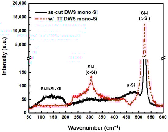
Figure 1.
Raman spectra before and after thermal treatment (TT) of as-cut monocrystalline Si (mono-Si) wafer manufactured via diamond wire sawing (DWS) method.
3.1.2. Gettering Effect
The results of the QSSPC measurements (Figure 2) showed that the bulk lifetime more than doubled as a result of thermal treatment (TT), increasing from 42.6 µs before the treatment to 93.8 µs after. Additionally, the overall PL lifetime intensity increased and was uniform after thermal treatment.
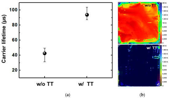
Figure 2.
Measurement of bulk lifetime via saw damage gettering (SDG) before and after TT: (a) QSSPC; (b) PL images.
These results confirmed that the SDG effect of utilizing saw marks on the wafer surface as gettering sites was realized even when the thermal treatment was conducted for only 10 min. Although SDG has been shown to increase the bulk lifetime in a variety of Si wafer materials [13], the process typically entails high temperatures (≥850 °C) and/or long durations of 80–180 h. In the present study, however, the bulk lifetime was improved after thermal treatment at 800 °C for only 10 min; this finding has significant implications for improving solar cell performance.
3.2. Effect of Thermal Treatment (TT) on Texturing of DWS mono-Si Wafers
3.2.1. Uniformity in Texture
The SEM images of the wafer surfaces show that random pyramids were formed on all of the different types of wafers upon texturing (Figure 3). However, the as-cut samples bore saw marks on their surfaces even after texturing (Figure 3c,d) whereas the heat-treated samples clearly exhibited uniform pyramidal textures over large surface areas (Figure 3e,f). The phase transformation layer, generated on the surface of Si wafers as a result of DWS, exhibited a non-uniform shape because the etch rate in this region was lower than that in the regions containing mono-Si wafers [14].
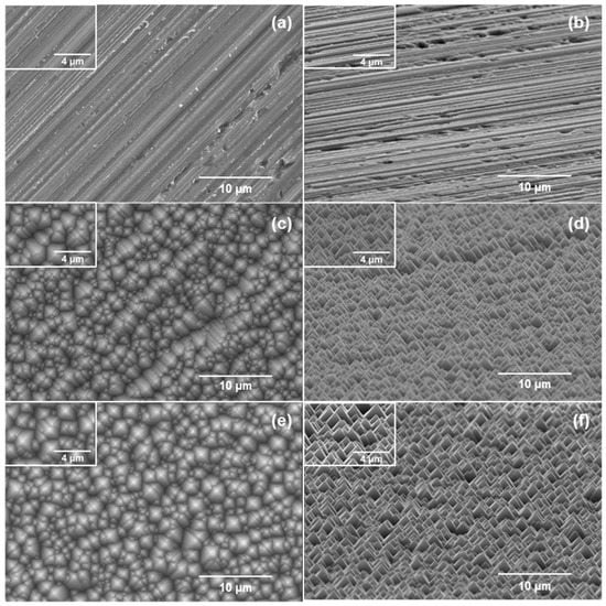
Figure 3.
Scanning electron microscopy (SEM) images of surfaces of DWS as-cut mono-Si wafers subjected to anisotropic texturing with or without TT: (a,b) as-cut samples; (c,d) samples textured without TT; (e,f) samples textured after TT. Images (a,c,e) offer top views. Images (b,d,f) present tilted views.
After texturing, the intercept method was used to define the pyramid size [6]. The intercept method is to draw diagonal lines on the SEM image and count the number of diagonal pyramids. The number of pyramids intersecting the line is counted. The average pyramids are found by dividing the number of intersections by the actual line length.
Figure 4 shows that the scale bar indicates 10 µm, the length of the line is 50 µm. As a result of the measurement, the pyramid size of the textured sample without thermal treatment is 1.6–1.9 µm and 1.8 µm after thermal treatment. After thermal treatment, these results clearly show that the surface condition before texturing affects the formation of the pyramid, and after the thermal treatment, a more uniform pyramid shape can be confirmed.
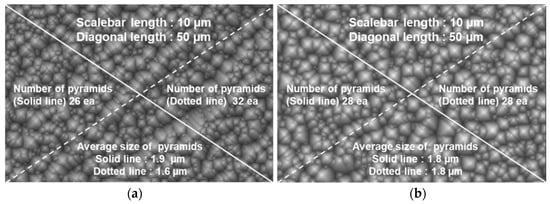
Figure 4.
Intercept method using SEM image: (a) without thermal treatment; (b) with thermal treatment after texturing.
Figure 5 shows that the etching after texturing was more uniform on the heat-treated samples in which the mono-Si phase on the surface was uniformly present than on the other Si wafers, which had a mixture of several layers on their surfaces as a result of DWS. Hence, more etching was performed in the same duration on the heat-treated samples than on the other wafers, and the variation in etching among the heat-treated wafers was low. The etching thickness was calculated using Equation (1) [15].
where is the decrease in wafer weight, is the wafer area, and is the density of silicon.
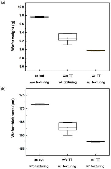
Figure 5.
Weight and thickness values of DWS mono-Si wafers: (a) Weight (g); (b) Thickness (µm).
3.2.2. Variation in Surface Reflectance
Equation (2) was used to calculate the value of weighted average reflectance (Rw) using the reflectance measured via UV–Vis spectroscopy [16,17].
where SAM1.5G is the solar spectral irradiance under an air mass (AM) of 1.5 G and R(λ) is the reflectance of the mono-Si wafer.
Figure 6 shows that the Rw of the mono-Si wafers in the as-cut state was 30.7%, which was slightly high. In the textured samples, this value decreased to 11.9% without thermal treatment and to a lower value of 11.2% when thermal treatment was conducted prior to texturing. This is a reflectance lower than the reference Rw range of 11.4–12.2% of a monocrystalline silicon wafer using anisotropic etching [18]. When SiNx was deposited as an ARC, the Rw of the mono-Si wafers in the as-cut state was 9.9%; this decreased even further to 3.4% in the samples textured without thermal treatment and 3.0% in the heat-treated and textured samples. The lower value of Rw of the heat-treated samples was a result of the ARC being more uniformly deposited on the uniform surface.
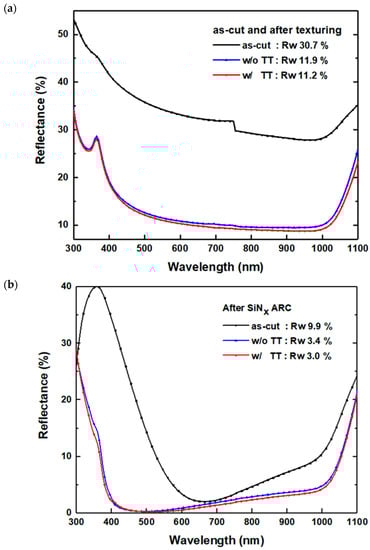
Figure 6.
Reflectance curves of DWS mono-Si wafers: (a) as-cut and textured; (b) after deposition of anti-reflection coating. The values of weighted average reflectance (Rw) in the wavelength range of 300–1100 nm are additionally shown.
In future work, we intend to employ SDG systematically at various temperatures and durations of thermal treatment to determine the optimum values of these operating parameters. Furthermore, we plan to fabricate a solar cell for a comparative analysis of the electrical characteristics of mono-Si wafers with and without saw marks.
4. Conclusions
Herein, we investigated a method for obtaining a uniform pyramidal surface over a large area of the textured surface of the DWS mono-Si wafer to increase its light absorption rate. Unlike conventional SDR, which entails significant consumption of chemical solution and several process steps, an effective and environment-friendly single-step process of thermal treatment was applied at 800 °C for 10 min. Thereafter, anisotropic texturing using DI water, KOH, and additive solutions was performed. The SEM measurements revealed that the saw marks present alongside the random pyramidal texture on the wafer surface were eliminated via thermal treatment, which converted the a-Si phase transformation layer on the wafer surface into the Si I (c-Si) phase. This ensured uniform etching rate and, hence, a uniform pyramidal texture was formed on the wafer surface. The Rw values of the textured DWS mono-Si wafers, with and without thermal treatment, were 11.2% and 11.9%, respectively, compared with that (30.7%) of the as-cut specimens, and decreased further to 3% and 3.4%, respectively, when ARCs were applied (Rw = 9.9% in as-cut state). Additionally, the SDG effect was realized using the saw marks on the DWS wafer surface as gettering sites during thermal treatment and, consequently, the bulk lifetime of the mono-Si wafer was more than doubled. The method developed in this study can be applied directly on an industrial scale without necessitating additional process equipment and will contribute to improvement in solar cell efficiency by enabling effective anisotropic texturing and improved wafer quality. In future work, we plan to employ SDG systematically to optimize the temperature and duration of thermal treatment as well as fabricate a solar cell to compare and analyze the electrical characteristics of wafers with and without saw marks.
Author Contributions
Conceptualization, Y.J.; data curation, Y.J.; formal analysis, Y.J.; experimentation, Y.J., K.M. and M.S.; writing–original draft, Y.J.; writing–review and editing, S.B.; supervision, Y.K. and H.L.; supervision, D.K. All authors have read and agreed to the published version of the manuscript.
Funding
This work was supported by the New & Renewable Energy Core Technology Program and Human Resources Program in Energy Technology of the Korea Institute of Energy Technology Evaluation and Planning (KETEP), and granted financial resources by the Ministry of Trade, Industry & Energy, Republic of Korea (Nos. 20193091010240 and 20204010600470). This work was also supported by the KU-KIST Graduate School Project.
Acknowledgments
The authors are grateful to the reviewers and editors for their helpful comments and suggestions.
Conflicts of Interest
The authors declare no conflict of interest.
References
- Lee, J.H.; Lim, D.K.; Lee, J.S. Principle of Solar Cell; Seoul Hong Reung Science Publish: Seoul, Korea, 2005. [Google Scholar]
- International Technology Roadmap for Photovoltaic (ITRPV) 11th ed. 2020. Available online: https://itrpv.vdma.org/web/itrpv/download (accessed on 13 April 2020).
- Basu, P.K.; Sreejith, K.P.; Yadav, T.S.; Kottanthariyil, A.; Sharma, A.K. Novel low-cost alkaline texturing process for diamond-wire-sawn industrial monocrystalline silicon wafers. Sol. Energy Mater. Sol. Cells. 2018, 185, 406–414. [Google Scholar] [CrossRef]
- Alasfour, A.; Yu, Z.J.; Weigand, W.; Quispe, D.; Holman, Z.C. Sub-micrometer random-pyramid texturing of silicon solar wafers with excellent surface passivation and low reflectance. Sol. Energy Mater. Sol. Cells. 2020, 218, 110761. [Google Scholar] [CrossRef]
- Verlinden, P.; Evrard, O.; Mazy, E.; Crahay, A. The surface texturization of solar cells: A new method using V-grooves with controllable sidewall angles. Sol. Energy Mater. Sol. Cells. 1992, 26, 71–78. [Google Scholar] [CrossRef]
- Park, H.; Kwon, S.; Lee, J.S.; Lim, H.J.; Yoon, S.; Kim, D. Improvement on surface texturing of single crystalline silicon for solar cells by saw-damage etching using an acidic solution. Sol. Energy Mater. Sol. Cells. 2009, 93, 1773–1778. [Google Scholar] [CrossRef]
- Costa, E.C.; Xavier, F.A.; Knoblauch, R.; Binder, C.; Weingaertner, W.L. Effect of cutting parameters on surface integrity of monocrystalline silicon sawn with an endless diamond wire saw. Sol. Energy 2020, 207, 640–650. [Google Scholar] [CrossRef]
- Kawasegi, N.; Morita, N.; Yamada, S.; Takano, N.; Oyama, T.; Ashida, K. Etch stop of silicon surface induced by tribo-nanolithography. Nanotechnology 2005, 16, 1411–1414. [Google Scholar] [CrossRef]
- Chen, K.; Liu, Y.; Wang, X.; Zhang, L.; Su, X. Novel texturing process for diamond-wire-sawn single-crystalline silicon solar cell. Sol. Energy Mater. Sol. Cells. 2015, 133, 148–155. [Google Scholar] [CrossRef]
- Stapf, A.; Honeit, F.; Gondek, C.; Kroke, E. Texturing of monocrystalline silicon wafers by HF-HCl-H2O2 mixtures: Generation of random inverted pyramids and simulation of light trapping in PERC solar cells. Sol. Energy Mater. Sol. Cells. 2017, 159, 112–120. [Google Scholar] [CrossRef]
- Acker, J.; Koschwitz, T.; Meinel, B.; Heinemann, R.; Blocks, C. HF/HNO3 etching of the saw damage. Energy Procedia 2013, 38, 223–233. [Google Scholar] [CrossRef][Green Version]
- Strapf, A.; Gondek, C.; Lippold, M.; Kroke, E. HF-(NH4)2S2O8-HCl mixtures for HNO3- and NOx-free etching of diamond wire- and SiC-slurry-sawn silicon wafers: Reactivity studies, surface chemistry, and unexpected pyramidal surface morphologies. ACS Appl. Mater. Interfaces 2015, 7, 8733–8742. [Google Scholar] [CrossRef] [PubMed]
- Shaw, E.C.; Hamer, P.; Collett, K.A.; Bourrett-Sicotte, G.; Bonilla, R.S.; Wilshaw, P.R. Saw damage gettering for industrially relevant mc-Si feedstock. Phys. Status Solidi A 2017, 214, 1700373. [Google Scholar] [CrossRef]
- Rao, R.; Bradby, J.E.; Williams, J.S. Patterning of silicon by indentation and chemical etching. Appl. Phys. Lett. 2007, 91, 123113. [Google Scholar] [CrossRef]
- Jung, Y.; Bae, S.; Lee, H.-S.; Kang, Y.; Kim, D. Effective Additive-Free Acidic-Solution Texturing for Surface-Damage-Free Kerfless Silicon Wafers. IEEE J. Photovolt. 2020, 10, 431–437. [Google Scholar] [CrossRef]
- Zhao, J.; Green, M.A. Optimized antireflection coatings for high-efficiency silicon solar cells. IEEE Trans. Electron. Dev. 1991, 38, 1925–1934. [Google Scholar] [CrossRef]
- Jung, Y.; Bae, S.; Lee, H.-S.; Kim, D.; Kang, Y. Novel double acidic texturing process for saw-damage-free kerfless multicrystalline silicon wafers. IEEE J. Photovolt. 2020, 10, 1545–1551. [Google Scholar] [CrossRef]
- Basu, P.K. Liquid silicate additive for alkaline texturing of mono-Si wafers to improve process bath lifetime and reduce IPA consumption. Sol. Energy Mater. Sol. Cells 2013, 113, 37–43. [Google Scholar] [CrossRef]


Publisher’s Note: MDPI stays neutral with regard to jurisdictional claims in published maps and institutional affiliations. |
© 2020 by the authors. Licensee MDPI, Basel, Switzerland. This article is an open access article distributed under the terms and conditions of the Creative Commons Attribution (CC BY) license (http://creativecommons.org/licenses/by/4.0/).