Article

SiC-Based High Efficiency High Isolation Dual Active Bridge Converter for a Power Electronic Transformer

Department of Electrical Engineering, University of Oviedo, 33204 Asturias, Spain
*
Author to whom correspondence should be addressed.
Energies 2020, 13(5), 1198; https://doi.org/10.3390/en13051198
Submission received: 30 January 2020 / Revised: 18 February 2020 / Accepted: 1 March 2020 / Published: 5 March 2020
(This article belongs to the Special Issue Design and Control of Power Converters 2020)

Abstract

:
This paper discusses the benefits of using silicon carbide (SiC) devices in a three-stage modular power electronic transformer. According to the requirements to be fulfilled by each stage, the second one (the DC/DC isolation converter) presents the most estimable improvements to be gained from the use of SiC devices. Therefore, this paper is focused on this second stage, implemented with a SiC-based dual active bridge. Selection of the SiC devices is detailed tackling the efficiency improvement which can be obtained when they are co-packed with SiC antiparallel Schottky diodes in addition to their intrinsic body diode. This efficiency improvement is dependent on the dual active bridge operation point. Hence, a simple device loss model is presented to assess the efficiency improvement and understand the reasons for this dependence. Experimental results from a 5-kW Dual Active Bridge prototype have been obtained to validate the model. The dual active bridge converter is also tested as part of the full PET module operating at rated power.

1. Introduction

A line-frequency transformer (LFT) is a key element in transmission and distribution for traditional centralized generation-based systems. Their main functionality is to interface different voltage levels in the grid [1]. LFTs are a well-established, relatively cheap, and reliable technology. However, they fail to cope with modern grid demands, such as the integration of distributed resources and energy storage systems, as well as power flow control.
The power electronic transformer (PET), also called a solid-state transformer (SST), was introduced in 1970 [2]. It is considered an alternative to LFT, as it connects two AC voltage ports while providing galvanic isolation [1]. PET is a semiconductor-based energy conversion system based on fast-switching devices, which potentially enables a significant reduction in volume and weight [3]. Moreover, thanks to the controllability of the power devices, the PET provides additional functionalities, such as reactive power, harmonics and imbalances compensation, ride-through capabilities, and smart protections.
The power semiconductor technology used in PETs has been traditionally based on Silicon (Si). However, the fast advances in wide-band-gap (WBG), specially the Silicon Carbide (SiC), power semiconductors has attracted the attention to their use in the medium voltage (MV) modular three-stage PETs [4], mainly due to their high blocking voltage along with their superior switching behavior [5,6].
Several examples of using SiC devices in different PET topologies exist in literature [7,8,9,10,11,12,13]. In the majority of applications, 1.2/1.7 kV commercial SiC MOSFETs are used for LV side devices, while for HV side, 10 kV non-commercial MOSFETs are used [6,8]. In some works, SiC was used in all the PET stages, such as in the TIPS (transformer-less intelligent power substation), which is an all-SiC three-stage PET topology [12]. In [14], a detailed comparison was carried out between two cases: (1) using 10 kV and 3.3 kV SiC MOSFETs and, (2) using 10 kV and 3.3 kV Si IGBTs, for different PET topologies. Authors concluded the importance of further research into the combined use of Si IGBT with SiC MOSFETs for three-stage PETs. Moreover, authors hinted at the importance of analyzing the relevance of including a SiC antiparallel diode to justify its additional cost implication.
Accordingly, the contribution of this paper is thought in two aspects:
  • Studying the requirements of the devices in each of the PET stages to assess the benefit of integrating SiC and, consequently, identifying the stages making best use of it.
  • Selection of the SiC devices for the second PET stage, based on a dual active bridge converter (DAB). As will be explained, this stage presents the most benefits from using SiC devices. Special attention will be paid to the device operation intrinsic to the converter topology. The use of SiC MOSFETs co-packaged with an additional SiC antiparallel diode is also investigated. A loss model is developed to estimate the potential efficiency improvement in this case. Both devices (i.e., with only intrinsic body diode and with additional SiC diode) are experimentally compared at rated power to validate the proposed model.
The paper is organized as follows: Section 2 describes the selected PET topology. Section 3 studies the integration of SiC devices in the different stages of the PET and identifies the practical limitations to the enhancements introduced by the use of these devices. Section 4 discusses the DAB converter development where the selection of the devices is detailed and the improvements introduced by using a SiC antiparallel diode is studied. Experimental results are provided in Section 5.

2. PET Topology

The selected PET topology is shown in Figure 1, and was previously discussed in [15,16,17,18,19,20]. It is a three-stage modular PET, with a Cascaded H-Bridge (CHB) converter acting as the front end AC/DC converter providing a HVAC link (VacHV). Each CHB cell integrates a DAB converter to provide the isolation between the HV and LV sides. Moreover, the integration of the DAB to the CHB cell provides the capability of bidirectional power transfer at the cell level [18,19]. The LV outputs of all DABs are connected in parallel to provide a high-current LVDC link (VdcLV), which is connected to a three-phase four-leg (3P4L) converter providing the LVAC link (VacLV).
As is clear in Figure 1, the structure is fully modular as it is formed by several identically-stacked cells. Thanks to this modular structure, the number of cells of the CHB is chosen in such a way that the cell voltage (Vcell) is equal to the required VdcLV. In this way the design of this DAB is, to some extent, simplified using a unity transformation ratio (i.e., no step-up/down).
This PET topology requires high galvanic isolation between HV and LV sides. The isolation is provided by the DAB high frequency transformer (HFT). Table 1 shows the characteristics of the developed PET.

3. Use of WBG for PET

The superior material properties of WBG semiconductors allow power devices to operate at higher temperatures, voltages and switching frequency in comparison to Si counterparts [4,21]. Among WBG materials, SiC presents the most mature technology for high voltage devices [4]. Both 1.2 kV and 1.7 kV SiC MOSFETs are already available on the market with a wide range of current ratings [5,22,23]. The use of SiC MOSFETs not only introduces a relevant improvement to the efficiency of fast switching power converters, but also enables going to higher switching frequencies at high blocking voltage which cannot be achieved using available Si IGBTs. However, at limited switching frequency requirements (<10 kHz), especially for high power (>100 A), Si IGBTs are still the preferred choice due to cost-effectivity and reliability in addition to SiC MOSFET higher dv/dt, di/dt, and EMI issues [24].
Accordingly, to analyze the merits of integrating SiC devices in the PET, the device requirements for each of the three stages of the PET are identified below.

3.1. Device Requirements per PET Stage

In the addressed PET topology, since no step-up/down is needed, the power devices employed on both transformer sides (i.e., HV and LV sides) have the same voltage rating. These include devices of the CHB full bridge (FB), the two DAB full bridges (FB1, FB2), and the DC/AC converter devices (see Figure 1). While this is true, the specifications in terms of current ratings and commutation requirements differ significantly.
CHB: its power devices do not need to commutate fast due to the multilevel nature of the topology [25,26]. Moreover, Ccell size is not determined by the cell switching frequency. Therefore, SiC switching devices are not of special merit here, even when going to higher Vcell (i.e., to reduce the number of stacked modules), still Si IGBT would be the selected option [14]. On the other hand, SiC free-wheeling antiparallel diodes are quite interesting in this case since the CHB full bridge is required to handle positive and negative currents (i.e., not only during the dead time). Therefore, SiC diodes can effectively improve the CHB efficiency due to their reduced conduction forward voltage drop as well as lower reverse recovery time compared to Si diodes [27].
DAB: high switching frequencies can provide significant reduction of the size and weight of the converter magnetics and the input and output capacitors. Additionally, going to higher PET module voltage is not achievable using Si devices, unless the switching frequency is reduced to few kHz. Regarding the antiparallel diode, the advantages of using SiC are still a controversial issue [14,28] and, therefore, will be analyzed in this work.
3P4L DC/AC: commutation requirements are not high (in the range of few kHz [29]), and since it interfaces the LVAC grid, high blocking voltages are not required. Therefore, Si devices are a good candidate for this stage.
Considering the above discussion, for this PET, 1.7 kV Si IGBT devices with SiC freewheeling diodes are used for the CHB FB. As for the DAB, 1.2 kV SiC MOSFETs are used and possible enhancements introduced by a SiC antiparallel diode will be discussed in detail in Section 4. Finally, 1.7 kV Si IGBTs are used for the 3P4L converter.
In the next section, the possible achievable enhancements gained by employing SiC in the DAB are discussed highlighting the practical limitations intrinsic to this PET topology.

3.2. Benefits and Practical Limitations of Using SiC MOSFETs for the DAB Converter

The use of SiC MOSFETs for the DAB converter in this PET structure has two main benefits:
  • It enables increasing the switching frequency of the DAB and, therefore, decreasing the size of the HFT [30,31].
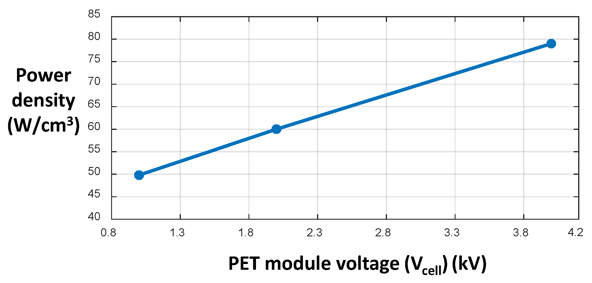
  • The high blocking voltages enable increasing Vcell and, therefore, for a given VacHV, the number of stacked PET modules can be reduced (see Figure 1) [7,17]. This is also advantageous for the HFT. Since each module handles more power, this leads to a higher transformer power density. In order to see clearly the effect of this, Figure 2 shows the HFT power density as a function of the cell voltage where the PET total power and VacHV are fixed (i.e., the number of PET modules vary). A comparative analysis regarding this relation is previously presented in [17] showing an improvement in the HFT power density as Vcell increases.
However, these SiC potential benefits may be compromised by certain practical implementation constraints.
On one hand, increasing Vcell has several adverse effects. High DC link voltages create practical problems for feeding the control circuitry in each cell. As commercial auxiliary power supplies (APS) do not provide the required isolation [29], each module circuitry has to be supplied from its DC link, where the HV and LV sides have separate APSs [32]. Commercial APSs can be used for voltages under 1 kV, otherwise, custom solutions must be implemented, such as the modular ISOP topology proposed in [29]. Consequently, various aspects must be considered for the selection of Vcell.
On the other hand, the size reduction of the HFT, in this particular case, is constrained by the high isolation required by the PET. This isolation imposes minimum clearance distances between windings, which compromises the window utilization factor resulting in a physical limit on further size reduction.

4. SiC-Based DAB Converter

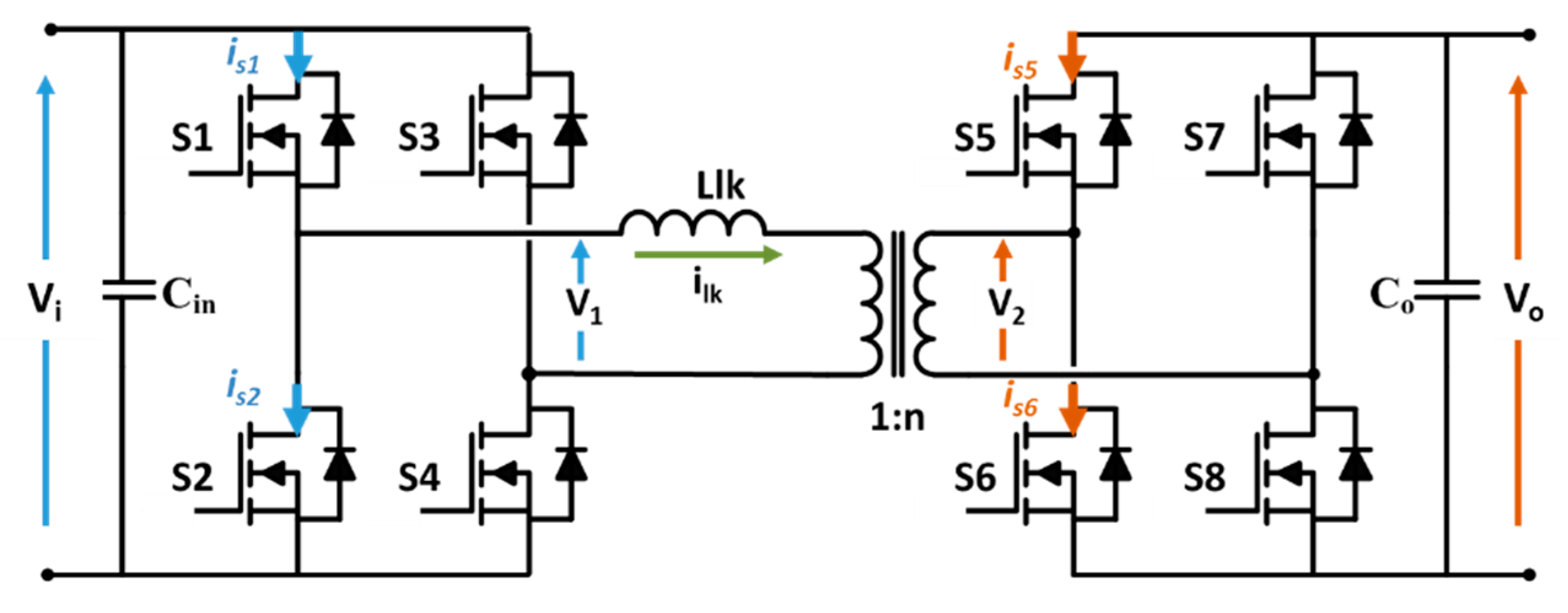
The DAB (see Figure 3) is selected for the intermediate stage of the PET, as it provides galvanic isolation as well as bidirectional power flow [33,34]. The DAB is based on two active bridges interfaced through an HFT, which provides the required galvanic isolation. This converter provides bidirectional operation by controlling the phase shift between the AC voltages generated by both bridges (V1 and V2). Also, this converter can have relatively high efficiency due to the soft-switching operation of all the devices at nominal conditions (zero-voltage switching, ZVS) [35,36].

4.1. SiC Device Selection

Regarding the selection of the SiC devices for the DAB, 6.5, 10, and 15 kV SiC MOSFETs have been reported for laboratory prototypes [37,38,39,40,41,42], but are far from being a viable commercial alternative yet. Current ratings offered in commercially available 1.7 kV SiC MOSFETs are still limited [23], and their commutation characteristic must be improved. The 1.2 kV SiC devices remain as the most mature technology available in the SiC device market. Consequently, these devices have been selected for the DAB. The DC link voltage is, therefore, set to 800 V.
Seven 1.2 kV SiC commercial MOSFETs were selected; two power modules and five discrete N-channel SiC MOSFETs. A comparative analysis of these devices was carried out in a boost converter operating in continuous conduction mode (CCM) (see Figure 4).
The boost converter was chosen as a preliminary test bench due to its simplicity and rapid prototyping, but foremost, due to its similar operation to a DAB converter as it has two switching devices in a leg with an inductance connected to the middle point. However, the differences in operation between a CCM boost and a DAB are well understood and, therefore, perspective devices resulting from the first selection stage are then tested in a DAB converter prototype.
The test bench used commercial driver boards from CREE and a commercial FPGA-based controller platform (BASYS2). Tests in the boost converter were done at 2 kW 400/800 V for switching frequencies of 30, 50, and 100 kHz and a dead time of 500 ns. Table 2 summarizes the results. The efficiency is calculated using the input and output DC voltages and currents of the converter measured using digital multimeters. It is observed that all the devices show a high efficiency barely affected by the increase in switching frequency which was increased by a factor of more than three.
Since the performance of all seven MOSFETs is comparable, the selection of the adequate option was mainly based on the size and the price. The specifications for the DAB converter are shown in Table 1. Accordingly, the peak current handled by the devices can be calculated from Equation (1) [35], where T is half the switching period, d is the phase shift, Llk is the leakage inductance, vo is the output voltage, vi is the input voltage and n is the HFT turns ratio:
I p _ l k = T 2 L l k ( 2 v o n d + v i v o n )
The current peak is calculated for the maximum phase-shift, this is selected to be 0.35 according to [35]. Based on Equation (1), this current is approximately equal to 11 A. The device current rating is selected to be twice the magnitude of the peak current handled by the devices to keep a safety margin. Therefore, the minimum required current rating is 22 A. This eliminates the two modules, and the CREE 60 A discrete, as the size and price are not justified in this case. The remaining four discrete devices are almost equally favored except for the ROHM SCH2080KE, as it includes a SiC Schottky barrier diode (SBD) co-packaged with the MOSFET.

4.2. Antiparallel SBD for a DAB Converter

Observing the efficiency of the boost converter using ROHM SCH2080KE versus for example ROHM SCT2080KE (without an additional SBD), it is consistently higher without SiC SBD. For the boost converter, this is logical as an additional antiparallel diode increases the output capacitance (see Table 2) and since hard-switching occurs, this increases the switching losses. Although, this makes sense and is simple to understand for the boost, for the DAB, it is more complicated as ZVS is implemented. That being the case, it is not valid to make a selection between both devices unless the additional diode behavior is studied for the DAB operation to identify if it improves or worsens its efficiency. This issue is addressed as follows, including: (1) understanding the potential effects introduced by a SiC antiparallel diode in a DAB converter, (2) developing a simple analytical loss model to estimate the possible efficiency improvement introduced by the SiC diode at a certain DAB operating point, and (3) validation of the proposed model using experimental results in a DAB prototype.
The two devices used in the analysis are the ROHM devices (i.e., SCH2080KE and SCT2080KE) as it is the same die but one packed with a SiC antiparallel SBD [22]. Characteristics of both devices are provided in Table 3. The diode forward voltage, VF-diode, is obtained from the datasheet at the value of Ip_lk (see Equation (1)) where the employed phase shift is that corresponding to 5 kW.

4.2.1. Advantages and Disadvantages of an Additional SBD

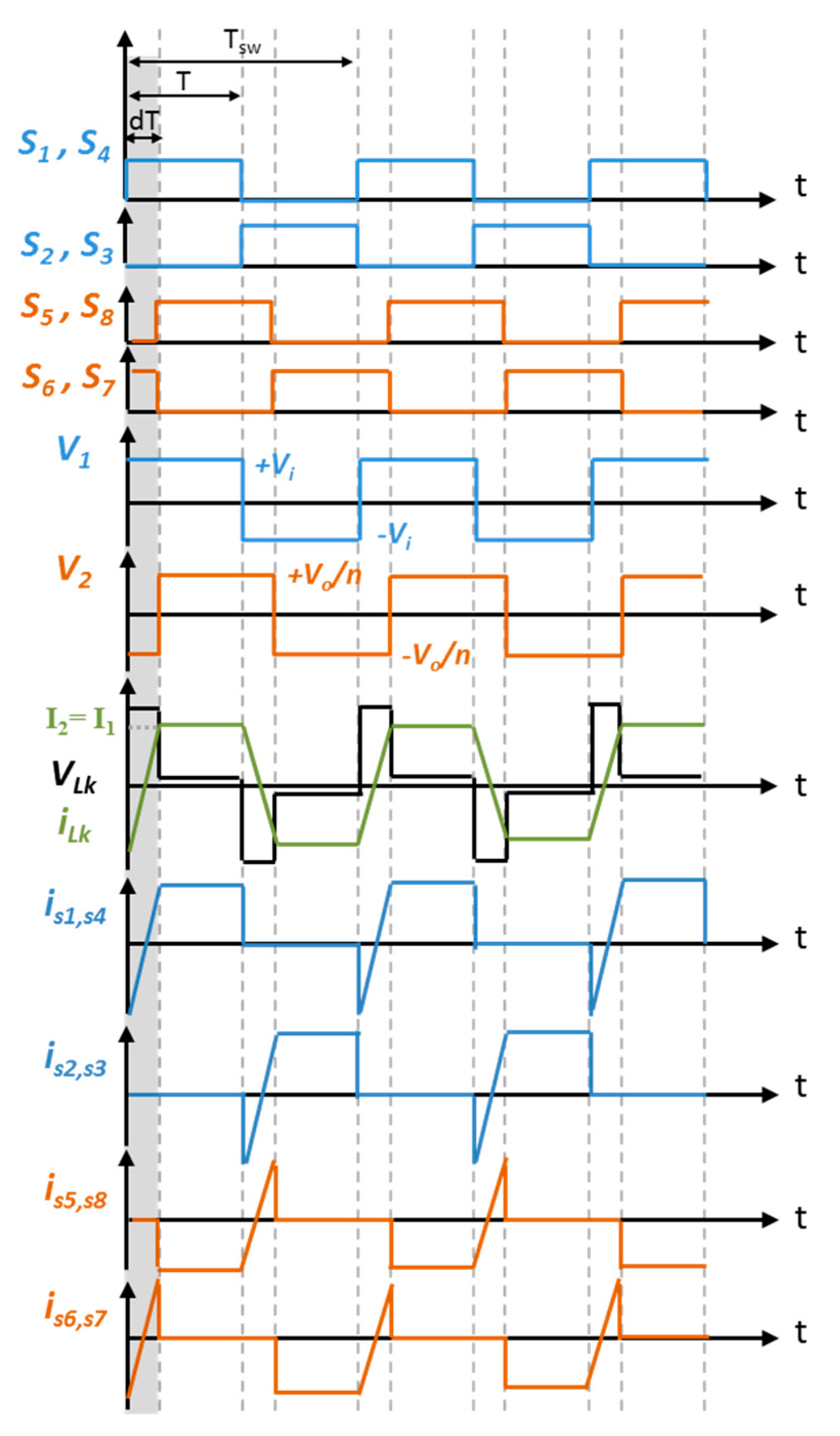
In order to provide a qualitative preliminary understanding of the possible effects of the SiC SBD on the DAB efficiency, the waveforms of the DAB are shown in Figure 5.
The potential advantages of using SCH2080KE +SBD in comparison to SCT2080KE are analyzed as follows:
  • Since VF-Diode of the additional SiC SBD is more than three times lower than that of the body diode (see Table 3), the power losses due to diode conduction during the dead times are lower using SCH2080KE +SBD.
  • The diode can enter into conduction while the MOSFET is ON. This can be seen from Figure 5, when the current through the MOSFET is negative (i.e., source to drain), a forward voltage drop, VF-MOSFET, is applied to the diode. If VF-MOSFET is higher than the diode knee voltage (Vknee), then the diode conducts. If this case is true, current is shared between the MOSFET and the diode and, therefore, conduction losses are reduced.
  • Unlike boost converter operation, soft switching is adopted in DAB devices at turn ON and, therefore, the additional output capacitance introduced by the additional SiC diode, illustrated in Figure 4, does not significantly penalize the switching losses (see Table 2).
However, these advantages can be compromised by several situations resulting in almost no advantages of having a SiC SBD, these cases are summarized as follows:
  • From Figure 6, diodes do not operate during the whole period of the dead time. During (A), the output parasitic capacitances of the MOSFETs (see Figure 4) in one leg are exchanging the voltage (i.e., one is discharging while the other is charging) and during (B), diodes conduct due to circulating currents. In some cases, (B) can tend to zero depending on the value of the current charging/discharging the parasitic capacitors and on the dead time.
  • If the current through the MOSFETs is not high enough to produce a VF-MOSFET > Vknee, then the diode will never conduct during MOSFET ON time.
  • The turn OFF switching losses should be analyzed as the enhancement introduced by the SiC SBD in the conduction losses can, in some cases, be compromised by the increase in turn OFF switching losses (due to the extra capacitance).
As a conclusion to the previous discussion, it is important to develop a simple model to determine, for a certain DAB operation point, if an extra antiparallel SiC diode co-packed with the SiC MOSFET is worthy or avoiding it is better. This is introduced in the next section.

4.2.2. Model to Assess the Efficiency Improvement Using a SiC Diode

Diode Conduction Intervals

Regarding diode conduction interval during the dead time, in order to estimate the time duration (B) (see Figure 6), the capacitor charging time during (A) is estimated using Equation (2), where Co(er) is the MOSFET effective output capacitance given by the data sheet and V1 = Vi = Vo. Accordingly, ilk is considered flat (I1 = I2 in Figure 5) and, therefore, as an approximation, the peak current (Ip_lk) is considered to be equal during all the switching transitions.
t ( A ) = 2 V 1   C o ( e r ) I p _ l k
Since t(B) = dead time − t(A), therefore diode operates for 570 ns for the case of the SiC SBD and 588 ns for the body diode. This time represents around 95% of the total dead time (600 ns) and, therefore, the reduction in conduction losses during diode operation is relevant to consider.
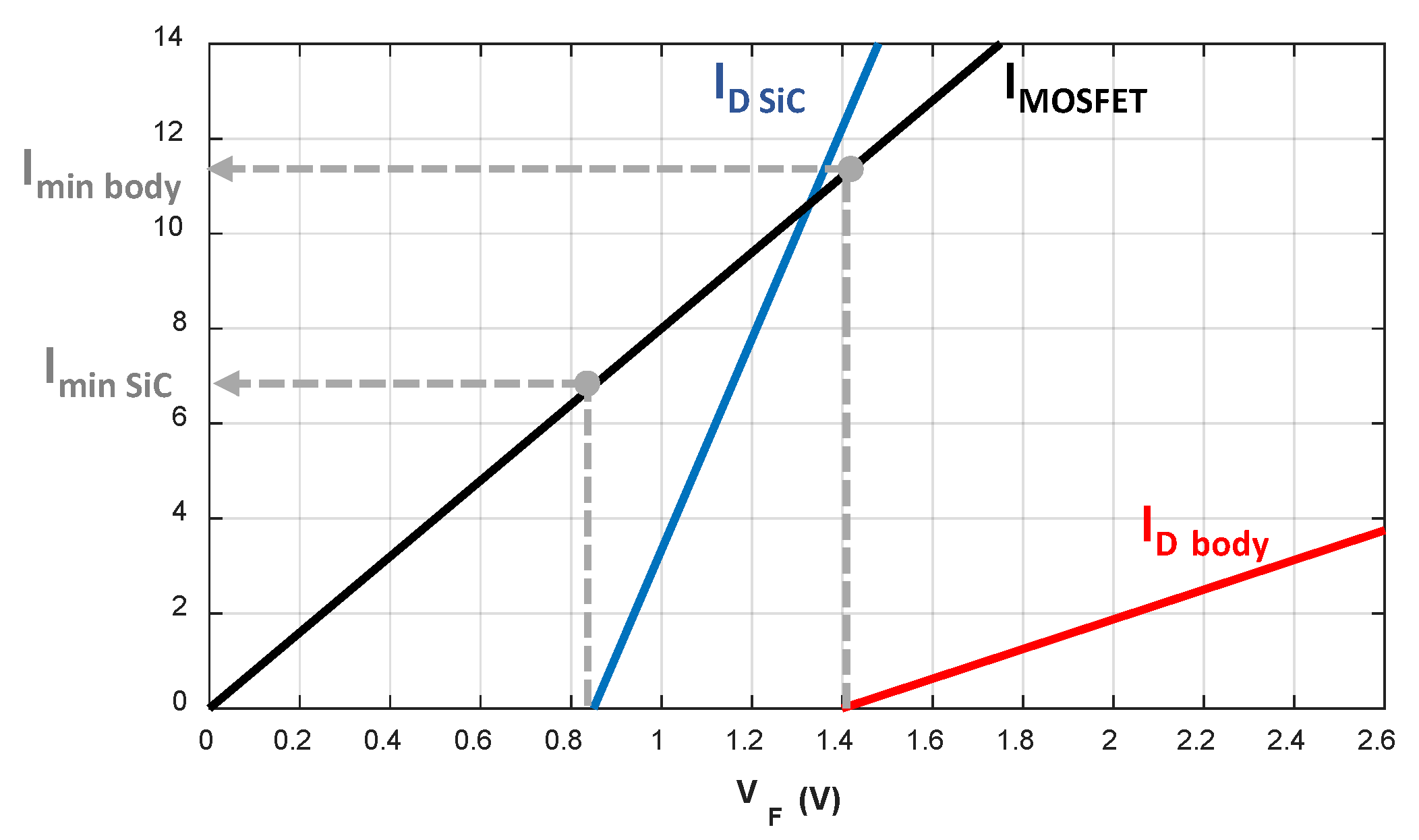
Regarding the diode conduction interval during MOSFET ON time, first, the diode characteristics are identified from the MOSFET datasheet (see Table 3). Figure 7 shows the forward voltage drop for both diodes (VF-Diode) as a function of the current through the diode. Additionally, the voltage drop on the MOSFET due to its ON resistance (VF-MOSFET) as a function of the current it is conducting is illustrated.
It is possible to see that each diode conducts when the current through the MOSFET is above a certain minimum value. It is clearly lower in the case of the SiC SBD. This can be estimated from Equation (3), where RON-MOSFET stands for ON-state drain-to-source MOSFET resistance:
I m i n = V k n e e R O N - M O S F E T
Based on the data in Table 3, Imin SiC is 6.8 A while Imin body is 11.2 A. Since the theoretical calculated Ip_lk = 9 A, therefore it is not possible that the body diode enters into conduction while the MOSFET is ON. On the other hand, the SiC diode would conduct when the current exceeds 6.8 A.

Estimation of the Power Losses

Power losses are estimated for both cases of the DAB using MOSFETs with a SiC antiparallel diode (SCH2080KE) and with only the body diode (SCT2080KE). Theoretical power loss estimation will be compared to the experimental efficiency results presented in the next section.
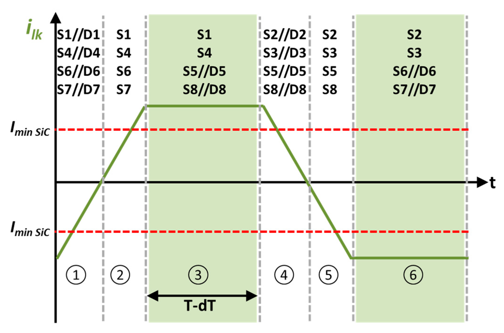
First, the periods where the diode can conduct (when it is forward biased) are identified as shown in Figure 8. It can be seen that, the diodes of all the ON MOSFETs can conduct during (1) and (4) as the current through all the devices is negative (see Figure 5), while during (3) and (6) only the diodes of the secondary bridge can conduct.
Accordingly, to simplify the power loss estimation the following assumptions are made:
  • As Imin SiC is around 75% of Ipk-lk, therefore, it is assumed that the diode operates only during period (3) and (6) when the peak current is passing through the devices (periods (1) and (4) are neglected).
  • The power loss estimation is performed only during the periods with different operation for the case of the SiC SBD and the body diode. In other words, only the difference in losses between both cases is considered. These intervals are: (3), (6) and the dead times.
During intervals (3) and (6), the conduction and switching losses of all the devices are estimated, while during the dead times, only the diodes conduction losses are estimated.
(a)Losses during dead time:
During one switching period (Tsw), four intervals of dead time take place. During each interval two diodes conduct. Accordingly, the diodes total conduction losses are estimated using Equation (4), where VF-Diode is the diode forward voltage at Ip_lk obtained from the diode characteristic curve given by the datasheet (linearized in Figure 7).
P d e a d t i m e = 8 · V F - D i o d e · I p _ l k · t ( B ) T s w
(b)Losses during interval (3) and (6) (Figure 8):
Losses during these two intervals are divided into: (1) turn OFF switching losses (Psw) and (2) MOSFET and diode conduction losses (PMOSFET and PDiode). The switching losses are straightforward, estimated from MOSFET EOFF using Equation (5).
P s w = 8 · E O F F · f s w
On the other hand, conduction losses are not straight forward. As noticed from Figure 8, in both (3) and (6) intervals, the primary bridge devices are different from the secondary ones. For example, during (3), for the primary, only the MOSFETs conduct (i.e., all the current flows through the MOSFETs, S1 & S4). In this case, four MOSFETs of the primary bridge conduct during (3) and (6) (two in each interval). Therefore, the total primary conduction losses can be easily estimated using Equation (6).
P M O S F E T - p r i m = 4 · I p _ l k 2 · R O N - M O S F E T · T d T T s w
However, for the secondary, the current is shared between the diode and the MOSFET (S5, D5 and S8, D8). Accordingly, the current conducted by each element has to be estimated. Since the voltage drop on the MOSFET is equal to the diode VF-Diode, then:
I M · R O N - M O S F E T = V k n e e + I D · R D
where IM and ID are the currents through the MOSFET and the diode respectively and RD is the diode dynamic resistance.
Since the current is shared by both elements, then, IM and ID can be obtained from Equations (7) and (8):
I M + I D = I p _ l k
Finally, the total conduction losses of the secondary bridge during Tsw can be calculated from Equations (9) and (10):
P M O S F E T - s e c = 4 · I M 2 · R O N - M O S F E T · T d T T s w
P D i o d e - s e c = 4 · I D · V F - D i o d e | I D · T d T T s w
The values of the power loss components estimated in this section are summarized in Table 4 where the enhancement to the DAB efficiency is estimated to be approximately 0.22% given the rated power is 5 kW.

4.2.3. Experimental Validation of the Proposed Loss Model

A DAB test bench was constructed and tests were performed at the nominal operation defined in Table 1 and the results are summarized in Table 5.
It was observed that the measured efficiency of the DAB converter composed of MOSFETs with an additional SiC antiparallel SBD is higher than that with only the body diode. The enhancement observed from the experimental results is around 0.3%, which validates the calculation introduced previously resulting in 0.22%. These results validate the proposed hypothesis and approach.

5. Experimental Results of the PET Module

The developed full-scale PET module is shown in Figure 9. Its structure is that schematically shown in Figure 1b. Table 6 summarize the main components of the PET module.

5.1. Developed HFT

One of the key aspects in the design of this HFT is the high galvanic isolation required between its primary and secondary sides, being 24 kV in this PET. This presents significant challenges compared to the ones considered in literature [43,44]. Moreover, the DAB power transfer inductance (Llk) is magnetically integrated in the HFT by making use of its series leakage inductance [43]. This reduces size and cost but, on the other hand, imposes additional constrains on the HFT design due to the required accuracy of Llk.
The HFT design is, therefore, a tradeoff between four variables: transferred power capability, temperature rise (i.e., losses), size and cost. Several design iterations are performed to achieve the required isolation with an acceptable tradeoff between these variables. The HFT design was previously presented in [45]. The main experimental validation tests are provided in this work for completeness.
Figure 10a shows laboratory developed HFT for test purposes and Figure 10b shows the final factory encapsulated HFT. A UU core structure is used typically selected in literature for separate winding [46,47]. The core ferrite material is selected to be Ferroxcube® 3C90 based on the DAB switching frequency [43]. An epoxy resin providing 15 kV/mm and exhibiting acceptable thermal conductance of 3 W/mK was used for encapsulation.
Figure 11 shows a schematic representation of the HFT design from ANSYS PEmag® software (Canonsburg, PA, USA).
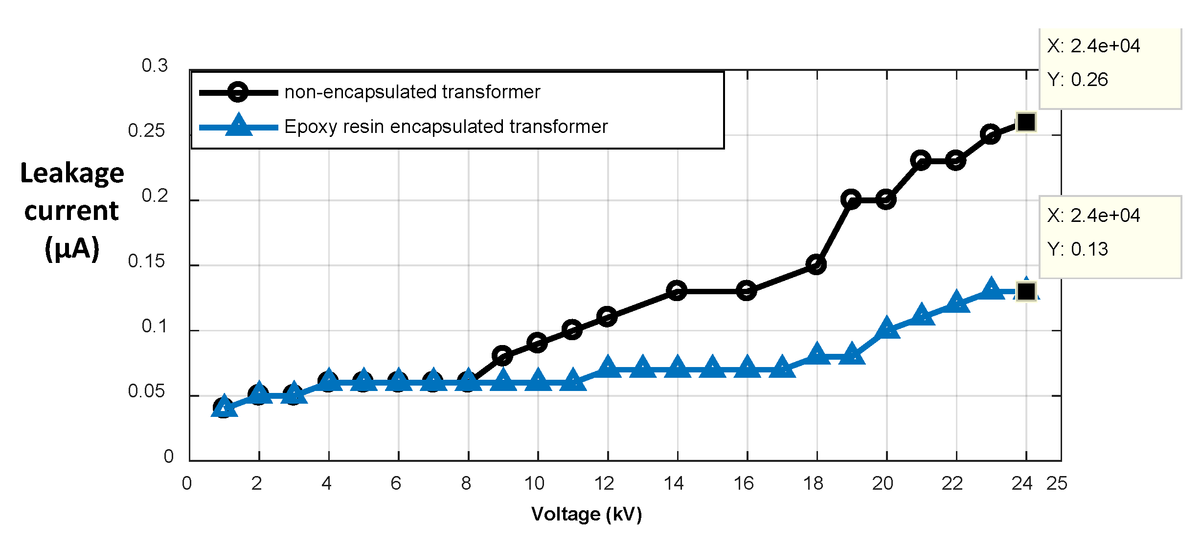
To verify the achieved isolation, a high potential test is done for both porotypes and results are compared. A Hipot tester is used to apply a voltage potential of up to 24 kV between both windings. The leakage current flowing from the winding with the higher potential, through air/resin, is recorded and shown in Figure 12. A significant diversion between both prototypes is clear at higher voltage potentials. Having lower leakage currents means that successive partial discharge due to high dv/dt is avoided which would lead to eventual insulation breakdown [48].
To locate the hottest spot and verify its temperature rise, five NTC sensors were mounted inside the HFT (see Figure 11). The location of this spot differs in encapsulated (NTC 1) and non-encapsulated prototypes (NTC 4). The temperature profile of the encapsulated HFT hottest spot during a four-hour DAB test at rated operation is shown in Figure 13. The steady state temperature, under natural convection, was recorded to be 60 °C.
A summary of the final HFT design is shown in Table 7.

5.2. Experimental Validation

Figure 14 shows the performed test connection diagram. A DC power supply is connected to the LVDC side to provide VdcLV and the power is transferred from FB2 to FB1. The DAB current control regulates the transferred power using single phase shift (SPS) modulation while the CHB full bridge regulates the cell capacitor voltage (Vcell).
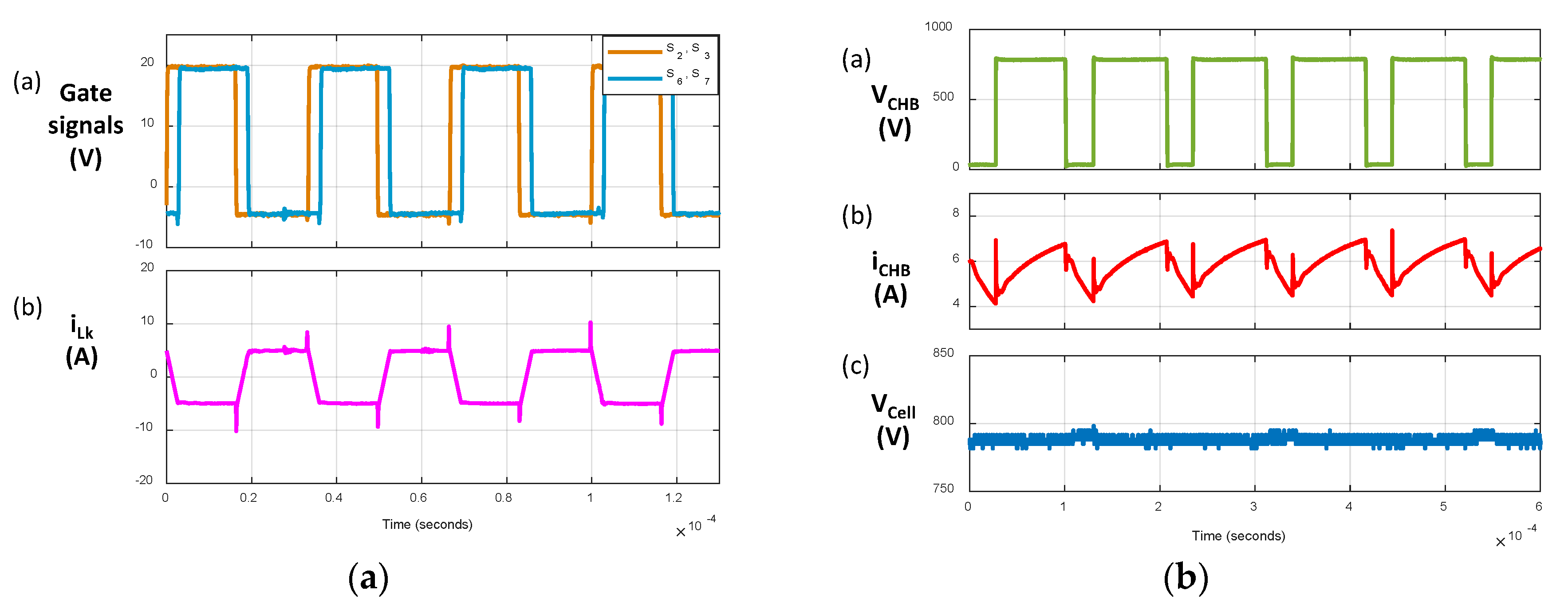
Figure 15 shows the experimental results for the PET module nominal operation (described in Table 1). Figure 15a shows the DAB waveforms, where FB2 gates are leading FB1 gates and the phase shift between both controls the magnitude of the transferred power [35].
Figure 15b shows the CHB waveforms, where VCHB and iCHB are the CHB full-bridge output voltage and current respectively. Vcell is regulated at 800 V by the CHB voltage control.

6. Conclusions

This paper analyzes the use of SiC devices in three-stage modular PETs. It has been shown that SiC MOSFETs can be especially advantageous in the isolation stage, as they combine high blocking voltage and high switching frequencies, leading to higher efficiency, size reduction of the isolation transformer, and higher power density. On the other hand, limited merit is achieved using SiC in the front end AC/DC and the LV side DC/AC converters. However, this partially depends on the application of the PET and the selected topology.
The paper details the selection of SiC MOSFETs for the DAB DC/DC isolation stage experimentally comparing different commercial devices. The benefits of a SiC antiparallel SBD is investigated. It is concluded that the SiC diode improves the efficiency of the DAB as it reduces the total conduction losses of the device. However, this improvement strongly depends on two critical design aspects: the employed dead time interval and the time interval during which the current is driven by both the MOSFET and the diode at the same time (due to the voltage drop in the MOSFET on resistance directly biasing the diode). Generally, the efficiency improvement can be more relevant for a flatter inductor current shape and when the DAB is working around its nominal operation point. A loss model was presented to assess the introduced efficiency improvement and was experimentally validated.
Experimental results showing the operation of the full-scale DAB converter at rated conditions as part of the PET module are provided.

Author Contributions

Conceptualization, A.R., M.A. and F.B.; methodology, A.R., M.A. and F.B.; software, M.S.; validation, M.S. and M.R.R.; formal analysis, M.S. and M.R.R.; investigation, M.S. and M.R.R.; writing—review and editing, M.S., M.R.R., A.R., M.A. and F.B.; supervision, A.R., M.A. and F.B.; funding acquisition, A.R., M.A. and F.B. All authors have read and agreed to the published version of the manuscript.

Funding

This work was supported by the Spanish Government under projects MCIU-19-RTI2018-099682-A-I00, FC-GRUPIN-IDI/2018/000179, and PAPI-18-PF-10 and by the European Commission FP7 Large Project NMP3-LA-2013-604057, under grant UE-14-SPEED-604057.

Conflicts of Interest

The authors declare no conflict of interest.

Nomenclature

VacHVHVAC grid voltage
VacLVLVAC grid voltage
VdcLVLVDC link voltage
CdcLVLVDC link capacitor
VcellCell capacitor voltage
CcellCell capacitor
fswSwitching frequency
THalf the switching period of the DAB
dPhase shift of the DAB represented as a ratio of T
LlkDAB leakage inductance
VkneeDiode knee voltage
VF-diodeDiode forward voltage
Ipk-lkPeak current through the leakage inductance
RON-MOSFETMOSFET ON resistance
Co(er)MOSFET effective output capacitance

References

  1. van der Merwe, J.W.; Mouton, H.d.T. The solid-state transformer concept: A new era in power distribution. In Proceedings of the AFRICON 2009, Nairobi, Kenya, 23–25 September 2009; pp. 1–6. [Google Scholar]
  2. McMurray, W. Power Converter Circuits Having a High-Frequency Link. U.S. Patent 3517300, 23 June 1970. [Google Scholar]
  3. Ronan, E.R.; Sudhoff, S.D.; Glover, S.F.; Galloway, D.L. A power electronic-based distribution transformer. IEEE Trans. Power Del. 2002, 17, 537–543. [Google Scholar] [CrossRef]
  4. Rothmund, D.; Ortiz, G.; Guillod, T.; Kolar, J.W. 10kV SiC-based isolated DC-DC converter for medium voltage-connected Solid-State Transformers. In Proceedings of the IEEE Applied Power Electronics Conference and Exposition (APEC), Charlotte, NC, USA, 15–19 March 2015; pp. 1096–1103. [Google Scholar]
  5. Millán, J.; Godignon, P.; Perpiñà, X.; Pérez-Tomás, A.; Rebollo, J. A Survey of Wide Bandgap Power Semiconductor Devices. IEEE Trans. Power Electron. 2014, 29, 2155–2163. [Google Scholar] [CrossRef]
  6. Millán, J.; Friedrichs, P.; Mihaila, A.; Soler, V.; Rebollo, J.; Banu, V.; Godignon, P. High-voltage SiC devices: Diodes and MOSFETs. In Proceedings of the International Semiconductor Conference (CAS), Sinaia, Romania, 12–14 October 2015; pp. 11–18. [Google Scholar]
  7. Dong, D.; Agamy, M.; Bebic, J.Z.; Chen, Q.; Mandrusiak, G. A Modular SiC High-Frequency Solid-State Transformer for Medium-Voltage Applications: Design, Implementation, and Testing. IEEE J. Emerg. Sel. Top. Power Electron. 2019, 7, 768–778. [Google Scholar] [CrossRef]
  8. Raju, R.; Dame, M.; Steigerwald, R. Solid-state transformer using silicon carbide-based modular building blocks. In Proceedings of the IEEE International Conference of Power Electronics and Drive Systems (PEDS), Honolulu, HI, USA, 12–15 December 2017; pp. 1–7. [Google Scholar]
  9. Yao, R.; Zheng, Z. Design and control of a SiC-based three-stage AC to DC power electronic transformer for electric traction applications. J. Eng. 2019, 2019, 2947–2952. [Google Scholar] [CrossRef]
  10. Wang, G.; Huang, X.; Wang, J.; Zhao, T.; Bhattacharya, S.; Huang, A.Q. Comparisons of 6.5kV 25A Si IGBT and 10-kV SiC MOSFET in Solid-State Transformer application. In Proceedings of the IEEE Energy Conversion Congress and Exposition (ECCE), Atlanta, GA, USA, 12–16 September 2010; pp. 100–104. [Google Scholar]
  11. Madhusoodhanan, S.; Tripathi, A.; Patel, D.; Mainali, K.; Kadavelugu, A.; Hazra, S.; Bhattacharya, S.; Hatua, K. Solid-State Transformer and MV Grid Tie Applications Enabled by 15 kV SiC IGBTs and 10 kV SiC MOSFETs Based Multilevel Converters. IEEE Trans. Ind. Appl. 2015, 51, 3343–3360. [Google Scholar] [CrossRef]
  12. Hatua, K.; Dutta, S.; Tripathi, A.; Baek, S.; Karimi, G.; Bhattacharya, S. Transformerless intelligent power substation design with 15 kV SiC IGBT for grid interconnection. In Proceedings of the IEEE Energy Conversion Congress and Exposition (ECCE), Phoenix, AZ, USA, 17–22 September 2011; pp. 4225–4232. [Google Scholar]
  13. Abu-Siada, A.; Budiri, J.; Abdou, A.F. Solid State Transformers Topologies, Controllers, and Applications: State-of-the-Art Literature Review. Electronics 2018, 7, 298. [Google Scholar] [CrossRef] [Green Version]
  14. Evans, N.M.; Lagier, T.; Pereira, A. A preliminary loss comparison of solid-state transformers in a rail application employing silicon carbide (SiC) MOSFET switches. In Proceedings of the 8th IET International Conference on Power Electronics, Machines and Drives (PEMD), Glasgow, UK, 19 April 2016; pp. 1–6. [Google Scholar]
  15. Lopez, M.; Briz, F.; Zapico, A.; Rodriguez, A.; Diaz-Reigosa, D. Control strategies for MMC using cells with power transfer capability. In Proceedings of the IEEE Energy Conversion Congress and Exposition (ECCE), Montreal, QC, Canada, 20–24 September 2015; pp. 3570–3577. [Google Scholar]
  16. Cuartas, J.M.; de la Cruz, A.; Briz, F.; Lopez, M. Start-up, functionalities and protection issues for CHB-based solid state transformers. In Proceedings of the IEEE International Conference on Environment and Electrical Engineering and IEEE Industrial and Commercial Power Systems Europe (EEEIC/I&CPS Europe), Milan, Italy, 6–9 June 2017; pp. 1–5. [Google Scholar]
  17. López, M.; Briz, F.; Saeed, M.; Arias, M.; Rodríguez, A. Comparative analysis of modular multiport power electronic transformer topologies. In Proceedings of the IEEE Energy Conversion Congress and Exposition (ECCE), Milwaukee, WI, USA, 18–22 September 2016; pp. 1–8. [Google Scholar]
  18. Briz, F.; Lopez, M.; Rodriguez, A.; Arias, M. Modular Power Electronic Transformers: Modular Multilevel Converter versus Cascaded H-Bridge Solutions. IEEE Ind. Electron. Mag. 2016, 10, 6–19. [Google Scholar] [CrossRef]
  19. Briz, F.; López, M.; Zapico, A.; Rodríguez, A.; Díaz-Reigosa, D. Operation and control of MMCs using cells with power transfer capability. In Proceedings of the IEEE Applied Power Electronics Conference and Exposition (APEC), Charlotte, NC, USA, 15–19 March 2015; pp. 980–987. [Google Scholar]
  20. European Union. “Silicon Carbide Power Technology for Energy Efficient Devices (SPEED)”, Ref. FP7-NMP3-LA-2013-604057, EU–FP7, Large Scale Integrating Collaborative Research Project. Available online: https://cordis.europa.eu/project/id/604057 (accessed on 4 March 2020).
  21. Wensong, Y. Wide Band-Gap Devices for Solid State Transformer Applications; Tutorial; FREEDM Systems Center: Raleigh, NC, USA, 2017. [Google Scholar]
  22. ROHM Semiconductor Electronics Industry Company. Available online: www.rohm.com (accessed on 2 March 2020).
  23. Wolfspeed, Inc. Available online: www.wolfspeed.com (accessed on 2 March 2020).
  24. Zhang, L.; Yuan, X.; Wu, X.; Shi, C.; Zhang, J.; Zhang, Y. Performance Evaluation of High-Power SiC MOSFET Modules in Comparison to Si IGBT Modules. IEEE Trans. Power Electron. 2019, 34, 1181–1196. [Google Scholar] [CrossRef]
  25. Malinowski, M.; Gopakumar, K.; Rodriguez, J.; Perez, M.A. A Survey on Cascaded Multilevel Inverters. IEEE Trans. Ind. Electron. 2010, 57, 2197–2206. [Google Scholar] [CrossRef]
  26. Rodriguez, J.; Lai, J.-S.; Peng, F.Z. Multilevel inverters: A survey of topologies, controls, and applications. IEEE Trans. Ind. Electron. 2002, 49, 724–738. [Google Scholar] [CrossRef] [Green Version]
  27. Sahib, A.; Abdulbaqi, I.M.; Ahmed, A.H. Analysis of a Four-Leg Inverter Feeding a Nonlinear Load using SVPWM Technique. In Proceedings of the Second Al-Sadiq International Conference on Multidisciplinary in IT and Communication Science and Applications (AIC-MITCSA), Baghdad, Iraq, 30–31 December 2017; pp. 19–24. [Google Scholar]
  28. Martin, D.; Killeen, P.; Curbow, W.A.; Sparkman, B.; Kegley, L.E.; McNutt, T. Comparing the switching performance of SiC MOSFET intrinsic body diode to additional SiC schottky diodes in SiC power modules. In Proceedings of the IEEE 4th Workshop on Wide Bandgap Power Devices and Applications (WiPDA), Fayetteville, AR, USA, 7–9 November 2016; pp. 242–246. [Google Scholar]
  29. Rodriguez, A.; Rogina, M.R.; Saeed, M.; Lamar, D.G.; Arias, M.; Lopez, M.; Briz, F. Auxiliary power supply based on a modular ISOP flyback configuration with very high input voltage. In Proceedings of the IEEE Energy Conversion Congress and Exposition (ECCE), Milwaukee, WI, USA, 18–22 September 2016; pp. 1–7. [Google Scholar]
  30. Huber, J.E.; Kolar, J.W. Solid-State Transformers: On the Origins and Evolution of Key Concepts. IEEE Ind. Electron. Mag. 2016, 10, 19–28. [Google Scholar] [CrossRef]
  31. McLyman, C.W.T. High Reliability Magnetic Devices: Design and Fabrication; Marcel Dekker: New York, NY, USA, 2002. [Google Scholar]
  32. Saeed, M.; Cuartas, J.M.; Rodriguez, A.; Arias, M.; Briz, F. Energization and Start-Up of CHB-Based Modular Three-Stage Solid-State Transformers. IEEE Trans. Ind. Appl. 2018, 54, 5483–5492. [Google Scholar] [CrossRef]
  33. de Doncker, R.W.; Divan, R.W.; Kheraluwala, M.H. A three-phase soft-switched high power-density dc/dc converter for high-power applications. IEEE Trans. Ind. Appl. 1991, 27, 63–73. [Google Scholar] [CrossRef]
  34. Kheraluwala, M.H.; Gascoigne, R.W.; Divan, D.M.; Baumann, E.D. Performance characterization of a high-power dual active bridge dc-to-dc converter. IEEE Trans. Ind. Appl. 1992, 28, 1294–1301. [Google Scholar] [CrossRef]
  35. Rodríguez, A.; Sebastian, J.; Lamar, D.G.; Hernando, M.M.; Vazquez, A. An overall study of a dual active bridge for bidirectional DC/DC conversion. In Proceedings of the IEEE Energy Conversion Congress & Exposition (ECCE), Atlanta, GA, USA, 12–16 September 2010; pp. 1129–1135. [Google Scholar]
  36. Calderon, C.; Barrado, A.; Rodriguez, A.; Alou, P.; Lazaro, A.; Fernandez, C.; Zumel, P. General Analysis of Switching Modes in a Dual Active Bridge with Triple Phase Shift Modulation. Energies 2018, 11, 2419. [Google Scholar] [CrossRef] [Green Version]
  37. Wang, G.; Huang, A.Q.; Wang, F.; Song, X.; Ni, X.; Ryu, S.H.; Grider, D.; Schupbach, M.; Palmour, J. Static and dynamic performance characterization and comparison of 15 kV SiC MOSFET and 15 kV SiC n-IGBTs. In Proceedings of the IEEE 27th International Symposium on Power Semiconductor Devices & IC’s (ISPSD), Hong Kong, China, 10–14 May 2015; pp. 229–232. [Google Scholar]
  38. Kumar, A.; Parashar, S.; Sabri, S.; van Brunt, E.; Bhattacharya, S.; Veliadis, V. Ruggedness of 6.5 kV, 30 a SiC MOSFETs in extreme transient conditions. In Proceedings of the IEEE 30th International Symposium on Power Semiconductor Devices and ICs (ISPSD), Chicago, IL, USA, 13–17 May 2018; pp. 423–426. [Google Scholar]
  39. Wang, L.; Zhu, Q.; Yu, W.; Huang, A.Q. A medium voltage bidirectional DC-DC converter combining resonant and dual active bridge converters. In Proceedings of the IEEE Applied Power Electronics Conference and Exposition (APEC), Charlotte, NC, USA, 15–19 March 2015; pp. 1104–1111. [Google Scholar]
  40. Wang, F.; Wang, G.; Huang, A.; Yu, W.; Ni, X. Design and operation of A 3.6kV high performance solid state transformer based on 13kV SiC MOSFET and JBS diode. In Proceedings of the IEEE Energy Conversion Congress and Exposition (ECCE), Pittsburgh, PA, USA, 14–18 September 2014; pp. 4553–4560. [Google Scholar]
  41. Pala, V.; Brunt, E.V.; Cheng, L.; O’Loughlin, M.; Richmond, J.; Burk, A.; Allen, S.T.; Grider, D.; Palmour, J.W.; Scozzie, C.J. 10 kV and 15 kV silicon carbide power MOSFETs for next-generation energy conversion and transmission systems. In Proceedings of the IEEE Energy Conversion Congress and Exposition (ECCE), Pittsburgh, PA, USA, 14–18 September 2014; pp. 449–454. [Google Scholar]
  42. Yun, C.-G.; Cho, Y. Active Hybrid Solid State Transformer Based on Multi-Level Converter Using SiC MOSFET. Energies 2019, 12, 66. [Google Scholar] [CrossRef] [Green Version]
  43. Mu, M.; Xue, L.; Boroyevich, D.; Hughes, B.; Mattavelli, P. Design of integrated transformer and inductor for high frequency dual active bridge GaN Charger for PHEV. In Proceedings of the IEEE Applied Power Electronics Conference and Exposition (APEC), Charlotte, NC, USA, 15–19 March 2015; pp. 579–585. [Google Scholar]
  44. Hoang, K.D.; Wang, J. Design optimization of high frequency transformer for dual active bridge DC-DC converter. In Proceedings of the XXth International Conference on Electrical Machines (ICEM), Marseille, France, 2–5 September 2012; pp. 2311–2317. [Google Scholar]
  45. Saeed, M.; Rogina, M.R.; Lopez, M.; Rodriguez, A.; Arias, M.; Briz, F. Design and construction of a DAB using SiC MOSFETs with an isolation of 24 kV for PET applications. In Proceedings of the IEEE 19th European Conference on Power Electronics and Applications (EPE’17 ECCE Europe), Warsaw, Poland, 11–14 September 2017; pp. P.1–P.10. [Google Scholar]
  46. Ortiz, G.; Biela, J.; Kolar, J.W. Optimized design of medium frequency transformers with high isolation requirements. In Proceedings of the IEEE IECON—36th Annual Conference on Industrial Electronics Society, Glendale, AZ, USA, 7–10 November 2010; pp. 631–638. [Google Scholar]
  47. Zhao, S.; Li, Q.; Lee, F.C. High frequency transformer design for modular power conversion from medium voltage AC to 400V DC. In Proceedings of the IEEE Applied Power Electronics Conference and Exposition (APEC), Tampa, FL, USA, 26–30 March 2017; pp. 2894–2901. [Google Scholar]
  48. Chen, Q.; Raju, R.; Dong, D.; Agamy, M. High Frequency Transformer Insulation in Medium Voltage SiC enabled Air-cooled Solid-State Transformers. In Proceedings of the IEEE Energy Conversion Congress and Exposition (ECCE), Portland, OR, USA, 23–27 September 2018; pp. 2436–2443. [Google Scholar]
Figure 1. Selected Power Electronic Transformer (PET) structure: (a) Three-stage modular PET topology based on a Cascaded H-Bridge (CHB) converter [17]. (b) One PET module composed of a Dual Active Bridge (DAB) and the full bridge of the CHB.
Energies 13 01198 g001
Figure 2. Theoretically calculated High Frequency Transformer (HFT) power density for three designs varying the Power Electronic Transformer (PET) module voltage (Vcell) and the handled power [17].
Energies 13 01198 g002
Figure 3. Dual active bridge (DAB) converter schematic.
Energies 13 01198 g003
Figure 4. Boost converter test bench schematic.
Energies 13 01198 g004
Figure 5. Dual Active Bridge (DAB) converter waveforms.
Energies 13 01198 g005
Figure 6. Waveforms of the gates and drain to source voltages of two MOSFETs in one leg during the dead time period.
Energies 13 01198 g006
Figure 7. MOSFET voltage drop and diode characteristic curve for the SiC Schottky Barrier Diode (SBD) and the body diode.
Energies 13 01198 g007
Figure 8. Current through the power transfer inductance of the Dual Active Bridge (DAB) showing periods where the antiparallel diode can enter into conduction mode during MOSFETs conduction.
Energies 13 01198 g008
Figure 9. The developed Power Electronic Transformer (PET) module.
Energies 13 01198 g009
Figure 10. High Frequency Transformer (HFT) prototype. (a) Non-encapsulated laboratory developed using 3D printed bobbins. (b) Encapsulated final HFT.
Energies 13 01198 g010
Figure 11. High Frequency Transformer (HFT) design taken from ANSYS PEmag®.
Energies 13 01198 g011
Figure 12. Experimental results. Leakage current measured between High Frequency Transformer (HFT) windings, as a function of the voltage difference between them.
Energies 13 01198 g012
Figure 13. Experimental results. Hottest spot temperature profile for the encapsulated High Frequency Transformer (HFT) using 3C90 ferrite core measured using a Negative Temperature Coefficient (NTC) sensor.
Energies 13 01198 g013
Figure 14. Schematic of the Power Electronic Transformer (PET) module during the performed experimental test.
Energies 13 01198 g014
Figure 15. Experimental results. (a) Dual Active Bridge (DAB) waveforms. Two gate signals of DAB FB1 and FB2 and leakage inductance current (ilK). (b) Cascaded H-Bridge (CHB) full bridge waveforms. CHB full bridge output voltage (VCHB), CHB full bridge output current (iCHB), and the cell capacitor voltage (Vcell).
Energies 13 01198 g015
Table 1. Main Power Electronic Transformer (PET) characteristics.
ElementParameterValue
PETRated power105 kW
Number of cells21 (7 per phase)
HV/LV grid voltage (L-L)6 kV/400 V
DABRated power5 kW
Switching frequency (fsw)30 kHz
HFT isolation24 kV
Input voltage (Vi = Vcell)800 V
Transformer turns ratio (n)1:1
Leakage inductance (Llk)423 μH
CHBRated power5 kW
Ccell600 µF(film)
Table 2. SiC MOSFET comparative analysis in a boost converter.
ManufacturerReferencePackageRated Current @100 °C (A)RDS (mΩ)Cout (pF)Efficiency (%)Price per Bridge (€)
30 kHz50 kHz100 kHz
STSCT30N120TO-247-334 80 130 97.7798.1697.81100
ROHMSCH2080KE + SBD28 80 175 97.7198.0297.69132
SCT2080KE28 807797.8298.1797.9380
CREEC2M0040120D40 4015097.7698.1097.84128
C2M0025120D60 2522097.5697.8897.42252
CAS120M12BM2 + SBD6-pack
45 mm
59 2540097.4997.5497.50412
CCS050M12CM2 + SBD Half-bridge
62 mm
138 1390096.4495.8-660
Table 3. Specifications of the compared devices.
CharacteristicsSCH2080KE +SBDSCT2080KE
RON-MOSFET125 mΩ
Eoff (Rg = 10 Ω)110 µJ120 µJ
Eon (Rg = 10 Ω)330 µJ275 µJ
Anti-parallel diodeTypeSiC SBDBody diode
RD (Estimated)45 mΩ320 mΩ
Vknee0.85 V1.4 V
VF-Diode (@ Ip_lk)1.2 V4.5 V
Table 4. Theoretically-estimated power losses.
IntervalLossesSCH2080KE +SBDSCT2080KE
Dead time (600 ns)Diode conduction (Pdeadtime)1.6 W6.2 W
(3) & (6)Switching (Psw)26.4 W28.8 W
ConductionPMOSFET-prim17.4 W17.4 W
PMOSFET-sec10.4 W17.4 W
PDiode-sec2.8 W-
Total losses58.6 W69.8 W
Table 5. Experimental results of the Dual Active Bridge (DAB) with and without SiC Schottky Barrier Diode (SBD).
CharacteristicsSCH2080KE +SBDSCT2080KE
Antiparallel diodeSiC SBDBody diode
Efficiency (η)98.1%97.8%
Phase-shift (d)0.29
Dead time600 ns
I p _ l k Calculated from Equation (1): 9 A
Measured (experimental): 9.8 A
Table 6. Main Power Electronic Transformer (PET) module components.
ElementCharacteristicsReference
DABROHM 1.2 kV, 28 A SiC MOSFETSCH2080KE
CREE 2-channel driversCGD15HB62P1
CHBInfineon 1.7 kV Si IGBT + SiC diodeNot commercial
Infineon two-channel drivers2ED300C17-S
ControllerXilinx FPGA (Spartan 3E) custom boardXC3S250E-4TQG144I
Table 7. High Frequency Transformer (HFT) design summary.
QuantityValue
Isolation24 kV
Core structureUU100/57/25
Ferrite materialFerroxcube® 3C90
EncapsulationEpoxy resin (15 kV/mm)
(ROYAPOX 912 THC/2)
BobbinsGPO-3 (20 kV/mm)
Number of turns (N)35
Temperature rise at NTC 440˚C