Article

± 180° Discontinuous PWM for Single-Phase PWM Converter of High-Speed Railway Propulsion System

1
Railroad Test & Certification Division, Korea Railroad Research Institute, Uiwang-si 16105, Korea
2
Smart Electrical & Signaling Division, Korea Railroad Research Institute, Uiwang-si 16105, Korea
3
Department of Railroad Electrical and Electronics Engineering, Korea National University of Transportation, Uiwang-si 16106
*
Author to whom correspondence should be addressed.
Energies 2020, 13(7), 1550; https://doi.org/10.3390/en13071550
Submission received: 26 February 2020 / Revised: 20 March 2020 / Accepted: 24 March 2020 / Published: 26 March 2020
(This article belongs to the Special Issue Design and Analysis of Electric Machines)

Abstract

:
As high-capacity alternating current/direct current (ac/dc) power conversion systems, single-phase pulse-width modulation (PWM) converters used in high-speed railway propulsion systems adopt high-voltage Insulated-Gate Bipolar Transistors (IGBTs) as switching elements. Due to their high breakdown voltage characteristics, the switching dynamics are inferior to those of low-voltage IGBTs and switching losses are more dominant than conduction losses despite operating at relatively low switching frequencies of hundreds to several kHz. To solve this problem, this paper proposes ± 180° discontinuous PWM (DPWM) suitable for a single-phase circuit. With the simple addition of offset voltages, the proposed DPWM method can be implemented easily and switching losses can be reduced by half by clamping the switching legs of the H-bridge converter to the positive or negative dc rail during every half cycle. In addition, temperature deviation between the power stacks can be minimized by using selective application of clamping modes. The validity and effectiveness of the proposed DPWM are verified through simulations and experiments of a prototype converter.

Graphical Abstract

1. Introduction

Recently, the number of personal vehicles globally has been increasing rapidly due to expeditious industrialization and urbanization, causing traffic congestion and environmental pollution. In tandem with efforts to solve this problem, the demand for eco-friendly and energy-efficient railway vehicles is increasing, and among them, high-speed railway (HSR) vehicles capable of high-speed and mass transportation are in the spotlight [1,2,3]. A high-speed railway propulsion system consists of a converter and a variable-voltage variable-frequency (VVVF) inverter to supply electric power to the traction system in the railway vehicles. Bi-directional H-bridge converters are widely used for both a unity power factor and constant direct current (dc)-link voltage controls [4]. They use high-voltage Insulated-Gate Bipolar Transistors (IGBTs) having low switching dynamic characteristics to handle high voltages and currents, resulting in high switching losses [4,5,6]. However, increased losses reduce the overall power conversion efficiency and are a burden on the design of the heat dissipation of the power converter. Therefore, low switching frequencies are used to keep switching losses below reasonable levels, which makes it difficult to expect a quick response to external disturbances including load and source variations. Meanwhile, recent advances in power electronics technology have enabled the use of relatively low breakdown voltage devices using multi-level converter topologies [7,8,9,10]. Multi-level converters have the advantage of having a high-power quality at relatively low switching frequencies due to their natural step-wise voltage waveform as well as the use of low breakdown voltage devices, but there are issues of increased circuit complexity and troublesome voltage balancing control. In the case of railway vehicles, the application of multi-level power systems has not yet become commonplace in the market because it is important to design the propulsion system to be as simple and robust as possible for the system reliability, safety of passengers, overall system cost, and maintenance convenience. On the other hand, a propulsion system using Silicon Carbide (SiC)-IGBT has been reported due to the recent development of power devices [11,12]. SiC-IGBT shows improved characteristics including fast switching dynamics, high breakdown voltage, low switching losses, and high thermal capacity over Si-IGBT. However, due to the low yield and high manufacturing cost, SiC-IGBT still needs more time to expand to the market. Therefore, the switching losses of power systems using simple two-level based high-voltage Si-IGBTs, such as HSR propulsion systems, should be reduced in different ways.
The classical carrier-based sinusoidal pulse-width modulation (CB-SPWM) determines the switching instant of each leg by comparing sinusoidal reference voltages with a triangular carrier [8]. Utilization of higher switching frequency creates more switching pulses, thus improving power quality and easing control of target values. However, it also increases switching losses. On the other hand, in a three-phase PWM inverter, various continuous and discontinuous modulation techniques can be implemented by adding an appropriate offset voltage [13,14,15,16,17,18]. Selecting the appropriate offset voltage can provide advantages such as reduced switching losses, improved waveform quality, and increased linear range. In particular, to reduce switching losses, switching legs can be clamped during one third of the period (120°) by using discontinuous PWM (DPWM) [14]. In general, DPWMs used in three-phase inverters are known to reduce switching losses by about 33% on average [18].
While there are various modulation techniques present for three-phase systems, the classical CB-SPWM is still widely used for single-phase systems due to the relative lack of modulation techniques. The basic idea of a suitable DPWM for a single phase system has been presented in [19]; however, no practical implementation methods or application areas have been described. Recently an application of DPWM for a single-phase PWM converter has been reported [20]. It can reduce switching losses by clamping the leg voltage for one third of a period, like the three-phase inverter, which has the advantage of equally distributed losses among switches and diodes. However, the loss reduction effect is limited, and the implementation is relatively complicated and not intuitive.
In this paper, we propose an effective ± 180° DPWM that is simple to implement and reduces switching loss by 50% compared to the existing CB-SPWM. The proposed method, which clamps either of two switching legs to positive or negative dc rails during a half power cycle, is naturally applicable to single-phase systems with two legs having 180° phase difference with each other. The proposed DPWM aims to generate an appropriate offset voltage to inhibit switching state changes in either of the two legs during the half power cycle, thereby reducing switching losses by half. The proposed method can be implemented in two ways. One is clamping the switching leg to the positive dc rail and the other is clamping it to the negative dc rail. By using these selective applications between two clamping methods, temperature deviation between power stacks can be minimized by the proposed DPWM. In this paper, we explain the basic idea of the proposed method, and suggest an offset voltage addition method that can be implemented easily. The operation characteristics of a single-phase PWM converter using the proposed DPWM and overall controller design were also considered. To verify the validity of the proposed method, a simulation was carried out and its effectiveness was confirmed by a 4 kW prototype circuit.

2. Conventional Carrier-Based Sinusoidal Pulse-Width Modulation (CB-SPWM) for Single-Phase PWM Converter of High-Speed Railway (HSR) Propulsion System

The HSR propulsion system is a power conversion system for driving and controlling a traction motor by receiving power from a catenary power source. It consists of a bi-directional PWM converter for a unity power factor and constant dc-link voltage controls and a VVVF inverter for driving the traction motor, as shown in Figure 1. The PWM converter is normally implemented by a full-bridge circuit capable of bi-directional power conversion during powering and regeneration modes. In HSR propulsion systems, it can also be composed of two interlaced full-bridge circuits for reducing input ripple current and sharing high conduction current. General rules for unity power factor control of the PWM converter are as follows. In the powering mode, a converter input voltage Vc, which is the difference in voltage between two leg voltages of Vuv and Vvy, lags behind the input voltage Vs to generate an input current Is having the same phase as Vs. On the other hand, in the regenerative mode, Vc is controlled to be ahead to Vs to generate Is having an opposite phase with Vs [21].
To generate those appropriate references for converter input voltages Vc*, a typical controller for the PWM converter consists of four parts, as shown in Figure 2. They include a phase-locked loop (PLL) for Vs, a voltage controller for sustaining constant dc-link voltage Vdc including a band rejection filter (BRF) to remove 120 Hz pulsation of the dc output stage, a current controller for shaping Is, and a PWM generator for making PWM switching pulses corresponding to Vc*. Since instantaneous control methods are usually used in the current controller, steady-state errors occur in systems having low control frequency bandwidth. To reduce these errors and improve the control response, the vector control methods in the dq synchronous coordinate system also can be utilized [22].
Figure 3a shows the PWM generation process using CB-SPWM. For the sinusoidal Vc*, two symmetric reference voltages for the switching legs, VUX* and VVY*, are determined as VUX* = Vc*/2 and VVY* = −Vc*/2, respectively, as shown in Equation (1).
V C * = V U X * V V Y * = ( V C * 2 ) ( V C * 2 ) .
In the single-phase PWM converter, the magnitudes of the two reference leg voltages are always the same. Therefore, the switching sequence resulting from CB-SPWM is symmetrical, as shown in Figure 4a. It is similar to the space vector PWM (SVPWM) in a three-phase PWM inverter, and either of two effective voltage vectors (01) and (10) is located symmetrically between two zero voltage vectors (00) and (11) in one switching sequence. Exact duration times for those effective and zero vectors are determined to satisfy the magnitude of Vc* on average during the single switching period Ts. In the switching pattern, “1” means that the upper switch is turned on and the lower switch is turned off in one leg, and “0” vice-versa. In the CB-SPWM method, a total of four switching state changes occur during Ts.

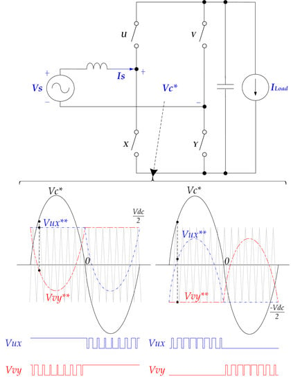
3. Proposed Discontinuous Pulse-Width Modulation (DPWM) for Single-Phase PWM Converter

3.1. Basic Idea for Proposed DPWM

As described above, two-level CB-SPWM uses two kinds of zero vectors (11) and (00), as shown in Figure 5a. This redundancy helps to reduce the ripple current of the inductor, but four switching state changes during the unit switching cycle cause increased switching losses. If only one of the two zero vectors is used, only two switching state changes occur during the same switching cycle, thereby reducing the switching losses by half. This idea can be implemented in two ways. One is called the upper clamping mode (UCM), which uses only the zero vector (11) and clamps Vux or Vvy to the positive dc rail, as shown in Figure 3b and Figure 4b. The general switching pattern of UCM is determined as shown in Figure 5b. The other is called the lower clamping mode (LCM), which utilizes only the zero vector (00) and fixes one of the two reference voltages to the negative dc rail, as shown in Figure 3c and Figure 4c. A typical switching pattern for LCM is shown in Figure 5c. These two clamping modes fix either of two reference voltages to a positive or negative dc rail during a half power cycle and this is referred to as ± 180° DPWM in this paper.
In UCM, as shown in Figure 3b, Vux** is fixed on the positive dc rail when Vc* > 0, and Vvy** is clamped on the positive dc rail when Vc* < 0. On the other hand, in LCM, shown in Figure 3c, Vux** is clamped to the negative dc rail when Vc* < 0 and Vvy** is locked to the negative dc rail when Vc* > 0. Here, Vux** and Vvy** are modified reference voltages for the UX and VY legs, respectively, in the proposed DPWM. As shown in Figure 4, the difference values between the two command voltages Vux* and Vvy* in CB-SPWM and between Vux** and Vvy** in DPWM are both preserved as Vc*. However, in DPWM using UCM, the larger of the two command voltages is clamped to the positive dc rail, and in LCM, the smaller command value is fixed to the negative dc rail. Looking at the switching patterns of the two clamping modes, the switching state change is reduced by half with utilization of only one of two zero vectors of (11) or (00), as shown in Figure 5b,c.

3.2. Implementation Method I: Direct Time Calculation

The proposed DPWM can be implemented in two ways. First, we will look at a direct time calculation method that calculates the dwelling times of adjacent vectors according to the position of the command voltage, similar to SVPWM applied to a three-phase inverter [23,24]. Given the converter command voltage Vc*, two adjacent vectors exist depending on the position of Vc*. When Vc* is positive, the adjacent vector is selected as a zero vector (11) or (00) located to the left of Vc* and an effective vector (10) located to the right of Vc*. The dwelling times T1 and T2 corresponding to the left vector V1 and the right vector V2, respectively, are determined to, on average, satisfy the magnitude of Vc* during one switching period. Equation (2) shows the calculation results of adjacent vectors dwelling times when Vc* is in region ①. On the other hand, when Vc* is located in the region ②, V1 becomes (01) and V2 becomes (11) or (00). When applying DPWM, either (11) or (00) is selected as a zero vector, according to the applied clamping modes. Table 1 shows the results of calculated dwelling times of adjacent vectors according to the position of Vc* and the PWM methods. The duration times of the switches U and V are equal to the sum of the dwelling times of adjacent vectors representing “1” in the switching pattern during Ts.
V C * T S = V 1 T 1 + V 2 T 2 , V 1 = 0 , V 2 = V d c , T 1 = V d c V C * V d c T S , T 2 = V C * V d c T S .

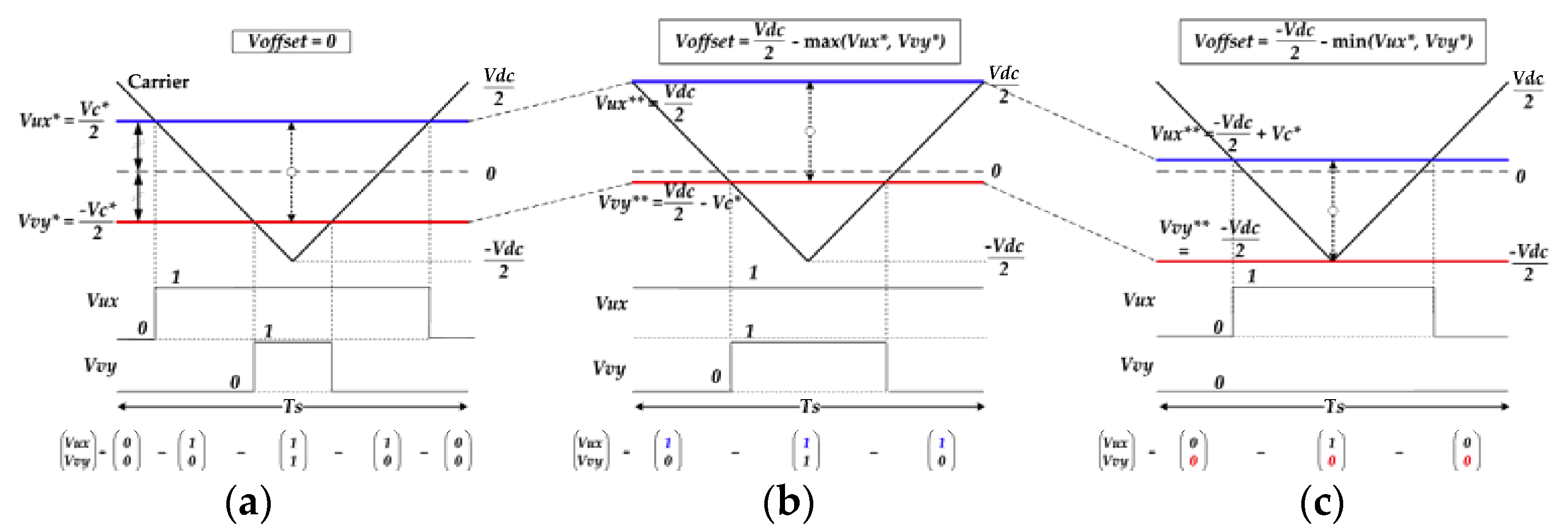
3.3. Implementation Method II: Offset Voltage Addition

The second method to implement the proposed DPWM is to apply the appropriate offset voltage to two leg command voltages Vux* and Vvy*. Equation (3) describes an offset voltage addition method.
V C * = V U X * V V Y * = ( V C * 2 ) ( V C * 2 ) = ( V C * 2 + V o f f s e t ) ( V C * 2 + V o f f s e t ) = V U X * * V V Y * * = upper   clamping   mode : { ( V d c 2 ) ¯ ( V d c 2 V C * ) ,    w h e n   V C * > 0   &   V o f f s e t = V d c 2 V C * 2 , ( V d c 2 + V C * ) ( V d c 2 ) ¯ ,    w h e n   V C * < 0   &   V o f f s e t = V d c 2 + V C * 2 , lower   clamping   mode : { ( V d c 2 + V C * ) ( V d c 2 ) _ ,    w h e n   V C * > 0   &   V o f f s e t = V d c 2 + V C * 2 , ( V d c 2 ) _ ( V d c 2 V C * ) ,    w h e n   V C * < 0   &   V o f f s e t = V d c 2 V C * 2 .
For a given reference voltage Vc*, the original UX and VY leg command voltages are determined as Vux* and Vvy* having equal magnitude and opposite sign for the symmetry of the single-phase system. Here, the modified reference voltages obtained by adding the appropriate offset voltage Voffset to Vux* and Vvy* are called Vux** and Vvy**, respectively. Since we added the same Voffset to Vux* and Vvy*, the difference between Vux** and Vvy** is the same as the original value Vc*. Depending on the type of Voffset, Vux and Vvy can be clamped to the positive or negative dc rail. Meanwhile, Vux** and Vvy** must be within the linear modulation range so that their magnitudes are limited as -Vdc/2 <|Vux(vy)**| < Vdc/2. Therefore, the possible applications of Voffset are limited to four cases, as shown in Equation (3), according to the polarity of Vc* while maintaining linear modulation.
To summarize these results, the maximum of Vux* and Vvy* can only be clamped to Vdc/2 and the minimum can only be clamped to −Vdc/2. Attempting to lock the maximum to −Vdc/2 or the minimum to Vdc/2 causes one of the Vux** and Vvy ** to fall outside the range of linear modulation. Thus, the suitable Voffset for clamping the switching leg to the positive or negative dc rails is simply determined by Equation (4). In the case of Voffset = Vdc/2-max(Vux*, Vvy*), it operates in UCM and if Voffset = −Vdc/2-min(Vux*, Vvy*), it is determined as LCM.
V o f f s e t = { V d c 2 max ( V U X * ,   V V Y * ) , V d c 2 min ( V U X * ,   V V Y * ) .
As expected, the results of the two implementation methods, the direct time calculation and the offset voltage addition methods, are the same. For example, when Vc* > 0 and UCM is applied, the effective duty of the switch V, dV, by the offset voltage addition method is calculated as Equation (5). The duty extraction process involves dividing the original reference value by Vdc for normalization and a + 0.5 level shift for positioning duty from 0 to 1. This is the same value of T1/Ts, where T1 is the corresponding value in Table 1. Therefore, in the following, the proposed DPWM will be described based on the offset voltage addition method, which is easier to implement.
d V = ( V d c 2 V C * V d c + 0.5 ) = 1 V C * V d c .

3.4. Mode Analysis

The circuit analysis of the proposed DPWM is the same as for the conventional two-leg PWM converter except that either of two switching legs is fixed to a positive or negative dc rail for every half power cycle. Figure 6 shows the main operation waveforms of the single-phase PWM converter using the proposed DPWM. With unity power factor control, the phase of Is equals to that of Vs, and Vc* lags to Vs. When UCM is applied, Vux** is clamped to Vdc/2 and Vvy** swings downward with a sinusoidal waveform in the range of Vux* > Vvy*. On the other hand, when Vux* < Vvy*, Vvy** is clamped to Vdc/2, Vux** swings downward. Meanwhile, when LCM is applied, Vvy** is clamped to −Vdc/2, Vux** swings upwards in the range where Vux* > Vvy*. On the other hand, when Vux* < Vvy*, Vux** is clamped at −Vdc/2, Vvy** swings upwards.
Figure 7 shows the equivalent circuits for each operation mode of the single-phase PWM converter using the proposed DPWM. Figure 7a–d show equivalent circuits operating in UCM, where the switches U or V are clamped to the positive dc rail during the single power cycle and the opposite non-clamped leg switches are switched in a PWM manner. In boosting mode, the inductor voltage VL becomes |Vs|, and thus the inductor current increases. In powering mode, VL becomes |Vs| − Vdc, which is negative, and thus the inductor current decreases to the contrary. In Figure 7e–h, equivalent circuits in LCM, the switches X or Y are clamped to the negative dc rail during a unit power cycle period, and the opposite leg switches are PWM-switched.

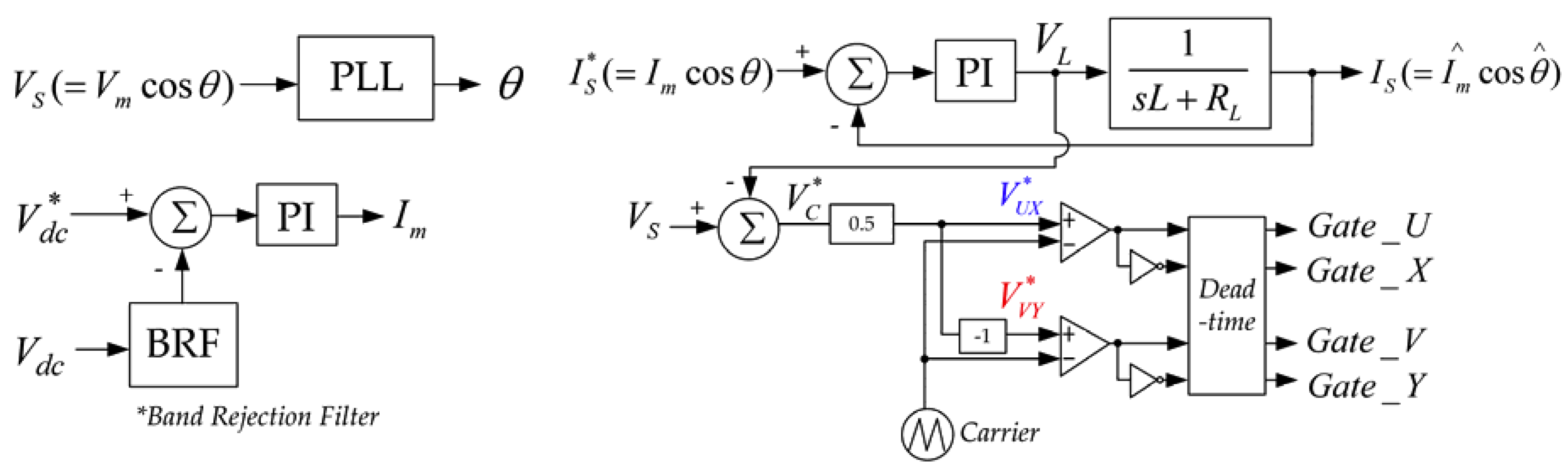
3.5. Controller Design for Proposed DPWM

Figure 8 shows the overall control block diagram for the single-phase PWM converter with the proposed DPWM. PLL of Vs for power factor control, constant voltage controller including BRF, all pass filters, and coordinate rotation conversion for vector current control in dq synchronous coordinate system are included. When the propulsion system is operated in powering mode, the output of the voltage controller becomes the d-axis current command of the current controller, which is positive, and the q-axis current command value is 0 for unity power factor control. In contrast, if it is operated in regenerative mode, the output of the voltage controller becomes negative to make Is have opposite phase with Vs. The output of the current controller Vc*, together with Vs and VL, is determined by Kirchhoff’s voltage law to satisfy the inductor voltage loop equation, as shown in Equation (6).
V d C e * = V d S e V d L e + ω L I q S e , V q C e * = V q S e V q L e ω L I d S e .
Here, the superscript e denotes a synchronous frame and the subscripts d and q represent d- and q-axis elements, respectively. ± ω L I q d S e are the cross coupling terms resulting from the rotation of the axis, ω is the angular frequency of Vs, and L is boost inductance. When Vc* is generated from the current controller, the appropriate Voffset for switching suppression is determined by the proposed DPWM technique, and the final leg command voltages Vux** and Vvy** are compared with the triangular carrier to output the gate signals Gate_U, Gate_X, Gate_V, and Gate_Y for PWM switching.

4. Simulation

4.1. Operation and Performance Verification

A Piecewise Linear Electrical Circuit Simulation (PLECS) simulation was performed to verify the operation of the proposed DPWM [25]. The circuit used in the simulation is the same as the single-phase PWM converter in Figure 1. In order to compare the performance and losses with the existing CB-SPWM, the actual datasheet-based IGBT thermal module provided in the PLECS software package was used [26]. Using the datasheet provided by the IGBT manufacturer, the conduction and switching losses of switching devices under actual operating conditions can be calculated [27]. The main characteristics of the IGBT used are the maximum allowable voltage Vce,max = 4500 V, the maximum allowable current Ic,max = 1200 A, and the maximum allowable junction temperature Tj,max = 125 °C. The main simulation parameters are shown in Table 2, which are based on the specifications of a PWM converter used in a propulsion system for a Korea power-concentrated HSR. The input inductance was selected considering both the ripple current at the rated power and the linear modulation range, and the dc-link capacitance was selected so that the voltage ripple at the rating is within ± 100 V. When implemented in DPWM, the switching frequency fsw of 1.08 kHz was chosen so that 18 pulses are produced within one cycle of the fundamental wave of 60 Hz.
Figure 9 compares the simulation results using DPWM and CB-SPWM. In both PWM schemes, the power factors of Vs and Is are more than 0.99. The total harmonic distortion of Is is 10.9% for DPWM and 5.6% for CB-SPWM. Vdc is well regulated at 2800 ± 100 V in both methods. In CB-SPWM, the final leg command voltages Vux** and Vvy** swing in a sinusoidal manner with the same magnitude and opposite phases to each other. On the other hand, in DPWM, Vux** and Vvy** are clamped to Vdc/2 or −Vdc/2 due to the addition of the Voffset voltage alternated between Vdc/2-max(Vux*, Vvy*) and −Vdc/2-min(Vux*, Vvy*) per every power cycle. The converter input voltage Vc shows 18 pulses during a half period in the SPWM and nine pulses in the DPWM. From the waveform shapes of Iu, Iv, Ix, and Iy, which are currents flowing through the switches U, V, X, and Y, respectively, when the DPWM is applied, two clamped switches are completely turned off or on per every power cycle period. The proposed DPWM alternates Voffset per every power cycle to reduce the deviation of conduction and switching losses of all switches. On the other hand, the clamping mode can be changed every half cycle, and the advantages resulting from the freedom of the clamping mode selection will be described in detail later. From the above results, the normal operation of the proposed DPWM method is verified.
Psw_igbt and Psw_diode mean summed switching losses of all IGBT switches and their body diodes, respectively, and Pcond_igbt and Pcond_diode are summed conduction losses of all IGBT switches and their body diodes, respectively. Psw_igbt includes turn-on and -off losses of IGBTs, and Psw_diode means reverse recovery losses of the body diodes. These results are summarized in Table 3. As expected, when operating at the same switching frequency, the switching losses of DPWM are reduced by half compared to CB-SPWM. Due to the characteristics of high-voltage IGBTs, switching losses account for an absolute portion of the total losses, which leads to a 45% reduction in total switches’ losses.

4.2. Ability to Reduce Temperature Deviations between Power Stacks

In large-power propulsion systems, the amount of power to be handled per unit power stack is very large, and thus separate heat-sinks or heat pipes are installed for each power stack for efficient heat-dissipation design. Therefore, the operating characteristics of the power stack may vary due to operating conditions or other external environmental factors. This difference in power stack characteristics results in unbalanced loss generation and temperature deviation between power stacks, which in turn affects the device lifetime, which is a key aspect of railway propulsion systems.
In conventional CB-SPWM PWM converters, this temperature imbalance cannot be controlled due to the symmetric operation between power stacks. In DPWM, on the other hand, there is redundancy in the clamping mode, as described above, and it can utilize the discriminative selection of the clamping mode to reduce the temperature deviation between the power stacks. The operating mode is alternated between UCM and LCM during every half power cycle; in other words, UCM is selected when Vc* > 0 and LCM when Vc* < 0. Switch U is fully conducting in UCM, and at the same time, switch X is completely off. On the other hand, U is completely turned off and X is completely conducting during LCM. As a result, U and X have minimal switching, while the switches V and Y must be switched continuously. Therefore, the temperature of the power stack including the U and X legs is lowered and that of the V and Y legs is relatively increased. Of course, the opposite clamping mode selection can be used to reverse the temperature changing pattern between the two power stacks.
By selecting the clamping mode every half cycle based on the temperature deviation, the temperature difference between the two power stacks can be minimized. Figure 10 is a flow chart showing the procedure for selecting different clamping modes based on temperature differences between power stacks. To suppress the excessive clamping mode change, the clamping mode is updated at the moment of Vc* crossing zero, i.e., every half cycle. Figure 11 shows the simulation results comparing the temperature deviation management capability. The simulation was performed by setting the initial temperature of V and Y stack, Temp_VY, to be 40 °C and that of U and X stack, Temp_UX, to be 25 °C. As can be seen from the results, the CB-SPWM cannot reduce the temperature deviation, while the DPWM reduces the temperature deviation rapidly by applying the selective clamping mode. When the proposed DPWM is applied, even in a steady state with little temperature deviation, the half of all IGBTs are clamped and stop switching during one cycle, and the clamped IGBTs cool down briefly. At the end of that clamped period, the temperature of the power stack containing those clamped IGBTs rises again by revived PWM switching. This temperature rising and falling phenomenon is repeated every two cycles, resulting in low-frequency thermal cycling of 30 Hz. Since such low frequency thermal cycling can shorten the lifetime of the IGBTs, thermal capacitance of the device junction to case, case to sink and heat-sink to ambient must be designed sufficiently large to withstand such low-frequency thermal cycling.

5. Experiment

Figure 12 shows the experimental prototype set of the single-phase PWM converter for verifying the normal operation of the proposed DPWM and compares its performance with CB-SPWM. The power stack is configured separately for each switch leg and the specific circuit configuration is equivalent to that of the PWM converter in Figure 1. An oscilloscope for observing Vs, Is, and bottom side gate signals Gate_X and Gate_Y, and a multi-meter for measuring output dc voltage are prepared. The actual load of the PWM converter for the railway vehicle is a traction motor driven by a VVVF inverter, but a suitable inverter and motor load for prototype testing are not prepared, thus a resistive load was used instead in this experiment. LeCroy’s MDA810 used in the experiment is a high-performance oscilloscope with bandwidth of 1 GHz, resolution of 12-bit, and sample rate of 2.5 GS/s, which outperforms existing 8-bit resolution products. However, it should be noted that the measurement accuracy is normally within ± 1%. The model name of used multi-meter is Fluke 177, which can measure from 30.0 mV to 1000 V with a resolution of 6000 counts, and the measurable ac frequency ranges from 2 Hz to 99.99 kHz. The load is a wound-type resistor with a fixed resistance value, including a cooling fan, which may contain a small inductance component that can affect in the kHz band, but the effect is negligible due to the high-frequency filtering of the filter capacitor. The test conditions are as follows: Vs is 220 V (ac rms), Vdc is 400 V (dc), L is 3.16 mH with series equivalent resistor, RL is 60 mΩ, Cdc is 3.06 mF. Switching frequency fsw is 5.4/2.7/1.8 kHz and the output power Po is 4 kW. Switches used in the experiments are Fuji Corporation’s high-voltage IGBT, 1MBI1200UE-330, having 3300 V/1200 A class.
Figure 13 shows the measured Vs, Is, Gate_Y, and Gate_X by varying fsw to 5.4 kHz, 2.7 kHz, and 1.8 kHz. The red, yellow, blue, and green lines denote Vs, Is, Gate_Y, and Gate_X, respectively. In the CB-SPWM, the PWM gate waveform changes sinusoidally, whereas in the DPWM, the UX or VY legs are clamped upward or downward every half power cycle. In all the results, the power factor of Vs and Is was over 0.96. The power conversion efficiency ƞ was calculated by the following Equation (7):
η = ( V d c , r m s ) 2 / R L o a d 1 T S < T S > ( V S · I S ) d t .
Here, Vdc,rms is rms value of Vdc and RLoad is the load resistance. The input power was calculated using the embedded function of the oscilloscope as the average value during one period of the product of the input voltage and current, and the output power was calculated as dividing the square of Vdc,rms by RLoad. As shown in Figure 14, the efficiency differences between CB-SPWM and DPWM were about 6.6% at fsw = 5.4 kHz (ƞ = 87.33% for CB-SPWM, 93.93% for DPWM), 2.98% at fsw = 2.7 kHz (ƞ = 94.14% for CB-SPWM, 97.12% for DPWM), 1.87% at fsw = 1.8 kHz (ƞ = 96.01% for CB-SPWM, 97.88% for DPWM). Due to the low dynamics of the high-voltage IGBTs, the efficiency decreases rapidly as fsw increases. In addition, since switching losses are more dominant than conduction losses in those IGBTs, the overall losses are reduced by almost half when DPWM is applied.

6. Conclusions

In this paper, a novel ± 180° DPWM is proposed to reduce switching losses of single-phase PWM converters used in HSR propulsion systems. The conventional PWM converter for railway application has large switching losses due to the use of a high voltage-rated IGBT device despite using relatively low switching frequency. To solve this problem, we modified the DPWM used in the three-phase inverter to devise a ± 180° DPWM suitable for a single-phase converter. By using the proposed modulation method, the switching state change can be reduced by half per every power cycle, and the switching losses can be reduced by half compared to the conventional CB-SPWM when operated at the same switching frequency. In addition, it has been shown that the offset voltage can be selectively applied every half power cycle to solve the temperature unbalance problem between the power stacks. Simulation and experiments confirmed normal operation of the proposed DPWM and it has been found that the total power conversion losses including switching losses can be greatly reduced by utilizing the proposed DPWM. The DPWM proposed in this paper is expected to be widely used in high power systems using high-voltage IGBTs as switching devices.

Author Contributions

Conceptualization, M.-S.S.; methodology, M.-S.S., I.-H.C., and J.-B.L.; software, J.-B.L.; validation, M.-S.S., I.-H.C., and J.-B.L.; formal analysis, M.-S.S.; experiments, M.-S.S., I.-H.C, and J.-B.L.; writing—original draft preparation, M.-S.S; writing—review and editing, M.-S.S. and I.-H.C. All authors have read and agreed to the published version of the manuscript.

Funding

This research was supported by a grant from the R&D program of the Korea Railroad Research Institute, Republic of Korea.

Conflicts of Interest

The authors declare no conflict of interest.

References

  1. Ronanki, D.; Singh, S.A.; Williamson, S.S. Comprehensive Topological overview of rolling stock architectures and recent trends in electric railway traction systems. IEEE Trans. Transp. Electr. 2017, 3, 724–738. [Google Scholar] [CrossRef]
  2. Lin, Y. Travel costs and urban specialization patterns: Evidence from China’s high speed railway system. J. Urban Econ. 2017, 98, 98–123. [Google Scholar] [CrossRef]
  3. Shao, Z.-Z.; Ma, Z.-J.; Sheu, J.-B.; Gao, H.O. Evaluation of large-scale transnational high-speed railway construction priority in the belt and road region. Transp. Res. Part E Logist. Transp. Rev. 2018, 117, 40–57. [Google Scholar] [CrossRef]
  4. Norrga, S. A soft-switched bi-directional isolated AC/DC converter for AC-fed railway propulsion applications. In Proceedings of the 2002 International Conference on Power Electronics, Machines and Drives (Conf. Publ. No. 487), Sante Fe, NM, USA, 4–7 June 2002. [Google Scholar]
  5. Uno, M.; Inoue, M.; Sato, Y.; Nagata, H. Bidirectional Interleaved PWM Converter with High Voltage-Conversion Ratio and Automatic Current Balancing Capability for Single-Cell Battery Power System in Small Scientific Satellites. Energies 2018, 11, 2702. [Google Scholar] [CrossRef] [Green Version]
  6. Kono, Y.; Ito, K.; Okawara, H.; Fukuma, T. Power electronics technologies for railway traction systems. Hitachi Rev. 2012, 61, 306–311. [Google Scholar]
  7. Feloups, C.E.S.; Ali, A.I.M.; Mohamed, E.E.M. Single-phase seven-level PWM inverter for PV systems employing multi-level boost converter. In Proceedings of the International Conference on Innovative Trends in Computer Engineering (ITCE), Aswan, Egypt, 19–21 March 2018. [Google Scholar]
  8. Akagi, H. Multilevel converters: Fundamental circuits and systems. Proc. IEEE 2017, 105, 2048–2065. [Google Scholar] [CrossRef]
  9. Akagi, H. Classification, terminology, and application of the modular multilevel cascade converter (MMCC). IEEE Trans. Power Electron. 2011, 26, 3119–3130. [Google Scholar] [CrossRef]
  10. Choudhury, A.; Pillay, P.; Williamson, S.S. Comparative analysis between two-level and three-level DC/AC electric vehicle traction inverters using a novel DC-link voltage balancing algorithm. IEEE J. Emerg. Sel. Top. Power Electron. 2014, 2, 529–540. [Google Scholar] [CrossRef]
  11. Ishikawa, K.; Yukutake, S.; Kono, Y.; Ogawa, K.; Kameshiro, N. Traction inverter that applies compact 3.3 kV/1200 A SiC hybrid module. In Proceedings of the 2014 International Power Electronics Conference (IPEC-Hiroshima 2014—ECCE ASIA), Hiroshima, Japan, 18–21 May 2014. [Google Scholar]
  12. Zhang, H.; Tolbert, L.M.; Ozpineci, B. Impact of SiC devices on hybrid electric and plug-in hybrid electric vehicles. IEEE Trans. Ind. Appl. 2011, 47, 912–921. [Google Scholar] [CrossRef]
  13. Holtz, J. Pulsewidth modulation—A survey. IEEE Trans. Ind. Electron. 1992, 39, 410–420. [Google Scholar] [CrossRef]
  14. Ojo, O. The generalized discontinuous PWM scheme for three-phase voltage source inverter. IEEE Trans. Ind. Electron. 2004, 51, 1280–1289. [Google Scholar] [CrossRef]
  15. Chung, D.W.; Kim, J.S.; Sul, S.K. Unified voltage modulation technique for real-time three-phase power conversion. IEEE Trans. Ind. Appl. 1998, 34, 374–380. [Google Scholar] [CrossRef]
  16. Hren, A.; Mihalic, F. An improved SPWM-based control with over-modulation strategy of the third harmonic elimination for a single-phase inverter. Energies 2018, 11, 881. [Google Scholar] [CrossRef] [Green Version]
  17. Blasko, V. Analysis of a hybrid PWM based on modified space-vector and triangle-comparison methods. IEEE Trans. Ind. Appl. 1997, 33, 756–764. [Google Scholar] [CrossRef]
  18. Hava, A.; Kerkman, R.; Lipo, T. A high performance generalized discontinuous PWM algorithm. IEEE Trans. Ind. Appl. 1998, 34, 1059–1071. [Google Scholar] [CrossRef]
  19. Holmes, D.G.; Lipo, T. Pulse Width Modulation for Power Converter: Principles and Practice, 1st ed.; John Wiley & Sons: New York, NY, USA, 2003; pp. 186–207. [Google Scholar]
  20. Yang, X.-J.; Qu, H.; Tang, H.J.; Yao, C.; Zhang, N.-Y.; Blaabjerg, F. Research on discontinuous pulse width modulation algorithm for single-phase voltage source rectifier. J. Int. Conf. Electr. Mach. Syst. 2014, 3, 433–445. [Google Scholar] [CrossRef] [Green Version]
  21. Mohan, N.; Undeland, T.M.; Robbins, W.P. Power Electronics-Converters, Applicaitons and Design; John Wiley & Sons: New York, NY, USA, 2003; pp. 243–244. [Google Scholar]
  22. Teodorescu, R.; Blaabjerg, F.; Liserre, M.; Loh, P.C. Proportional-resonant controllers and filters for grid-connected voltage-source converters. IEEE Proc. Electr. Power Appl. 2006, 153, 750–762. [Google Scholar] [CrossRef] [Green Version]
  23. Leon, J.I.; Portillo, R.; Franquelo, L.G.; Vazquez, S.; Carrasco, J.M.; Dominguez, E. New space vector modulation techniques for single-phase multilevel converters. In Proceedings of the 2007 IEEE International Symposium on Industrial Electronics, Vigo, Spain, 4–7 June 2007. [Google Scholar]
  24. Song, M.-S. Single-phase PWM converter for high-speed railway propulsion system using discontinuous PWM. J. Korean Soc. Railw. 2017, 20, 448–457. [Google Scholar] [CrossRef]
  25. The Simulation Platform for Power Electronic Systems. Available online: https://www.plexim.com/plecs (accessed on 30 January 2020).
  26. Thermal Simulation. Available online: https://www.plexim.com/plecs/thermal (accessed on 30 January 2020).
  27. Isidori, A.; Rossi, F.M.; Blaabjerg, F.; Ma, K. Thermal loading and reliability of 10-MW multilevel wind power converter at different wind roughness classes. IEEE Trans. Ind. Appl. 2014, 50, 484–494. [Google Scholar] [CrossRef]
Figure 1. Circuit diagram of conventional single-phase pulse-width modulation (PWM) converter for high-speed railway (HSR) propulsion system.
Energies 13 01550 g001
Figure 2. Control block diagram of conventional PWM converter using instantaneous current controller including phase-locked loop (PLL), voltage controller, and PWM generator.
Energies 13 01550 g002
Figure 3. Switching references according to the PWM methods: (a) conventional carrier-based sinusoidal pulse-width modulation (CB-SPWM), (b) proposed discontinuous PWM (DPWM) with upper clamping mode (UCM), and (c) proposed DPWM with lower clamping mode (LCM).
Energies 13 01550 g003
Figure 4. Typical switching sequence according to the PWM methods: (a) conventional CB-SPWM, (b) proposed DPWM with UCM, and (c) proposed DPWM with LCM.
Energies 13 01550 g004
Figure 5. Typical switching patterns according to the utilization of zero vectors: (a) two zero vectors are used, (b) only (11) zero vector is used in UCM, and (c) only (00) zero vector is used in LCM.
Energies 13 01550 g005
Figure 6. Main waveforms of single-phase PWM converter using proposed DPWM (from Top, Vs, Is; Carrier, Vux*, Vvy*, Voffset; Carrier, Vux**, Vvy**; Vux, Vvy).
Energies 13 01550 g006
Figure 7. Equivalent circuits for DPWM based single-phase PWM converter during one power cycle when adopting UCM (ad), and LCM (eh).
Energies 13 01550 g007aEnergies 13 01550 g007b
Figure 8. Overall control diagram of single-phase PWM converter using proposed DPWM.
Energies 13 01550 g008
Figure 9. Simulation waveforms of single-phase PWM converter using (a) proposed DPWM and (b) conventional CB-SPWM (from top, Vs, Is; Vdc; Vux*, Vvy*, Voffset; Vux**, Vvy**, Carrier; Vux, Vvy; Vc; Iu, Ix; Iv, Iy; Psw_igbt, Psw_diode, Pcond_igbt, Pcond_diode).
Energies 13 01550 g009
Figure 10. Clamping mode selection procedure according to power stack temperatures.
Energies 13 01550 g010
Figure 11. Comparison of temperature variation reduction ability between (a) proposed DPWM and (b) conventional CB-SPWM (from top, Vs, Is; Vux, Vvy; Temp_UX, Temp_VY).
Energies 13 01550 g011
Figure 12. Prototype circuit of single-phase PWM converter.
Energies 13 01550 g012
Figure 13. Comparisons of experimental main waveforms utilizing CB-SPWM (ac) and proposed DPWM (df).
Energies 13 01550 g013
Figure 14. Efficiency comparisons according to PWM methods and switching frequencies.
Energies 13 01550 g014
Table 1. Adjacent vectors and their dwelling times for CB-SPWM and DPWM.
Regions
Adjacent VectorsLeft: V1
Right: V2
0
Vdc
Vdc
0
Dwelling TimeT1
T2
(VdcVC*)/Vdc·TS
VC*/Vdc·TS
VC*/Vdc·TS
(Vdc + VC*)/Vdc·TS
PWM duration time for U
PWM duration time for V
(0 ~ TS)
CB-SPWMT1/2 + T2
T1/2
T2/2
T1 + T2/2
DPWMUpper clampingTS
T1
T2
TS
Lower clampingT2
0
0
T1
Table 2. Parameters used in simulation.
Main Parameters
Input voltage, Vs1400 V ac(rms)/60 HzOutput voltage, Vdc2800 V
Input inductance, L2 mHDC-link capacitance, Cdc6.26 mF
Output power, Po1 MWSwitching frequency, fsw1.08 kHz
Table 3. Comparison of switches’ losses between DPWM and CB-SPWM.
DPWMCB-SPWM
Psw_igbt [kW]6.3712.88
Psw_diode [kW]2.044.51
Pcond_igbt [kW]0.640.68
Pcond_diode [kW]2.152.12
Total loss [kW]11.0119.76

