Design Method of Dual Active Bridge Converters for Photovoltaic Systems with High Voltage Gain

 , , and
Abstract
:1. Introduction
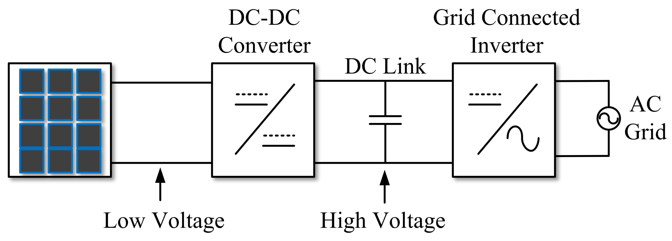
2. Analyses and Methods
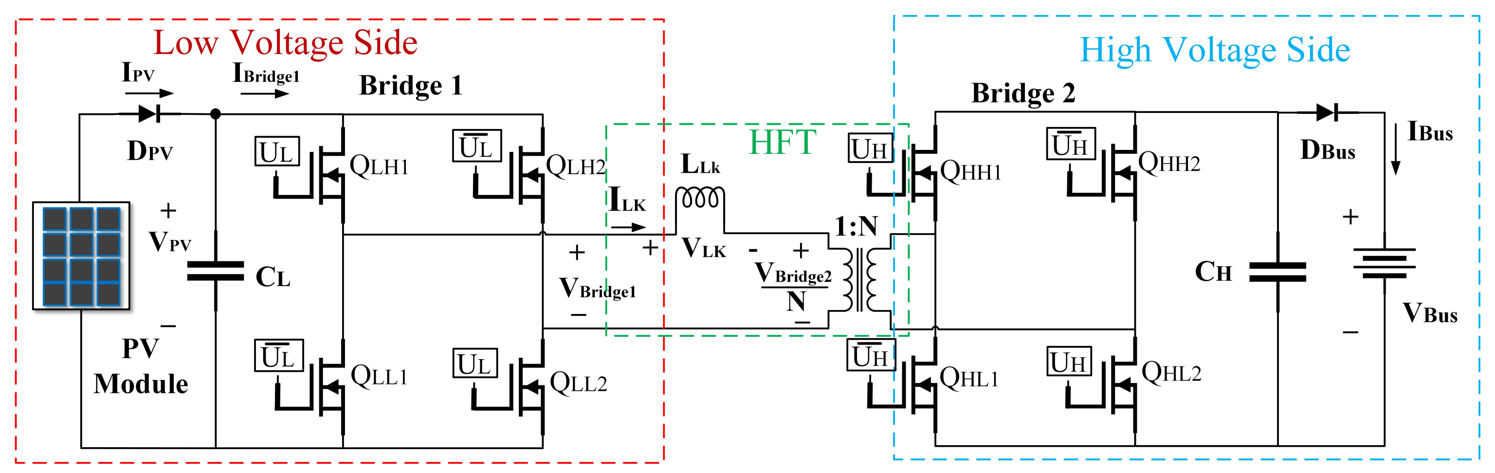
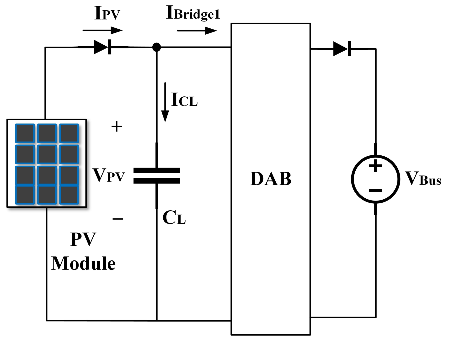
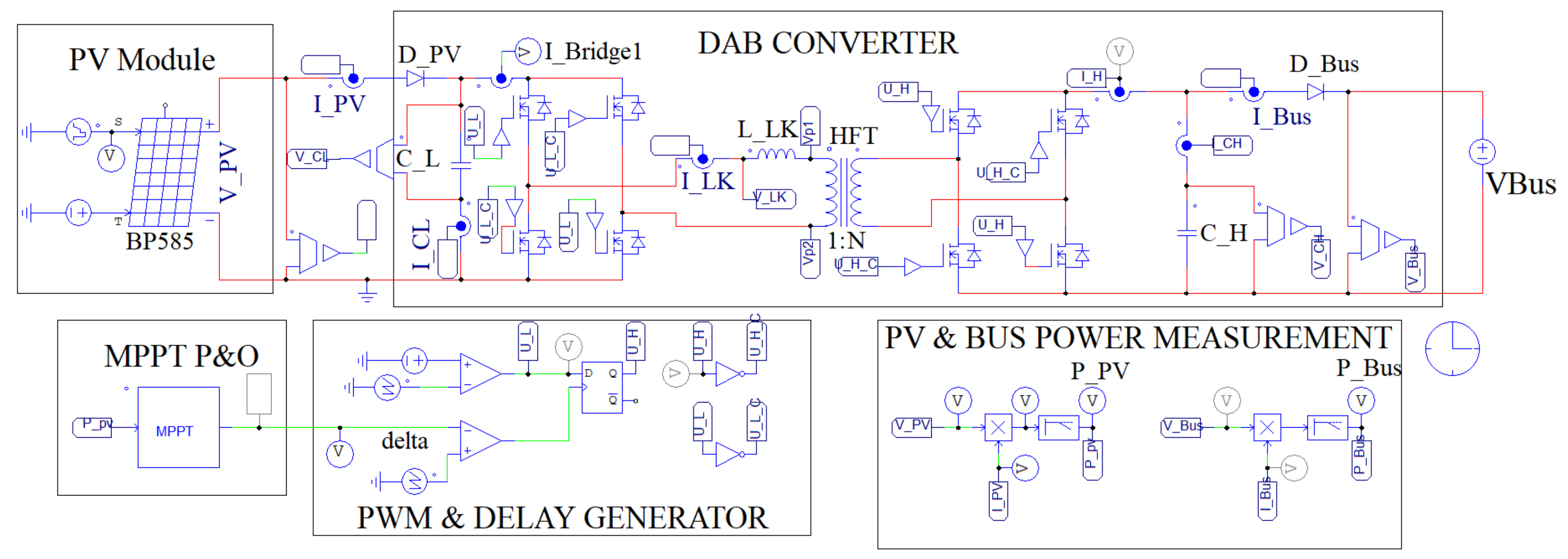
2.1. Analysis of the DAB Circuit
2.2. Analysis of the PV Module and DAB Connection
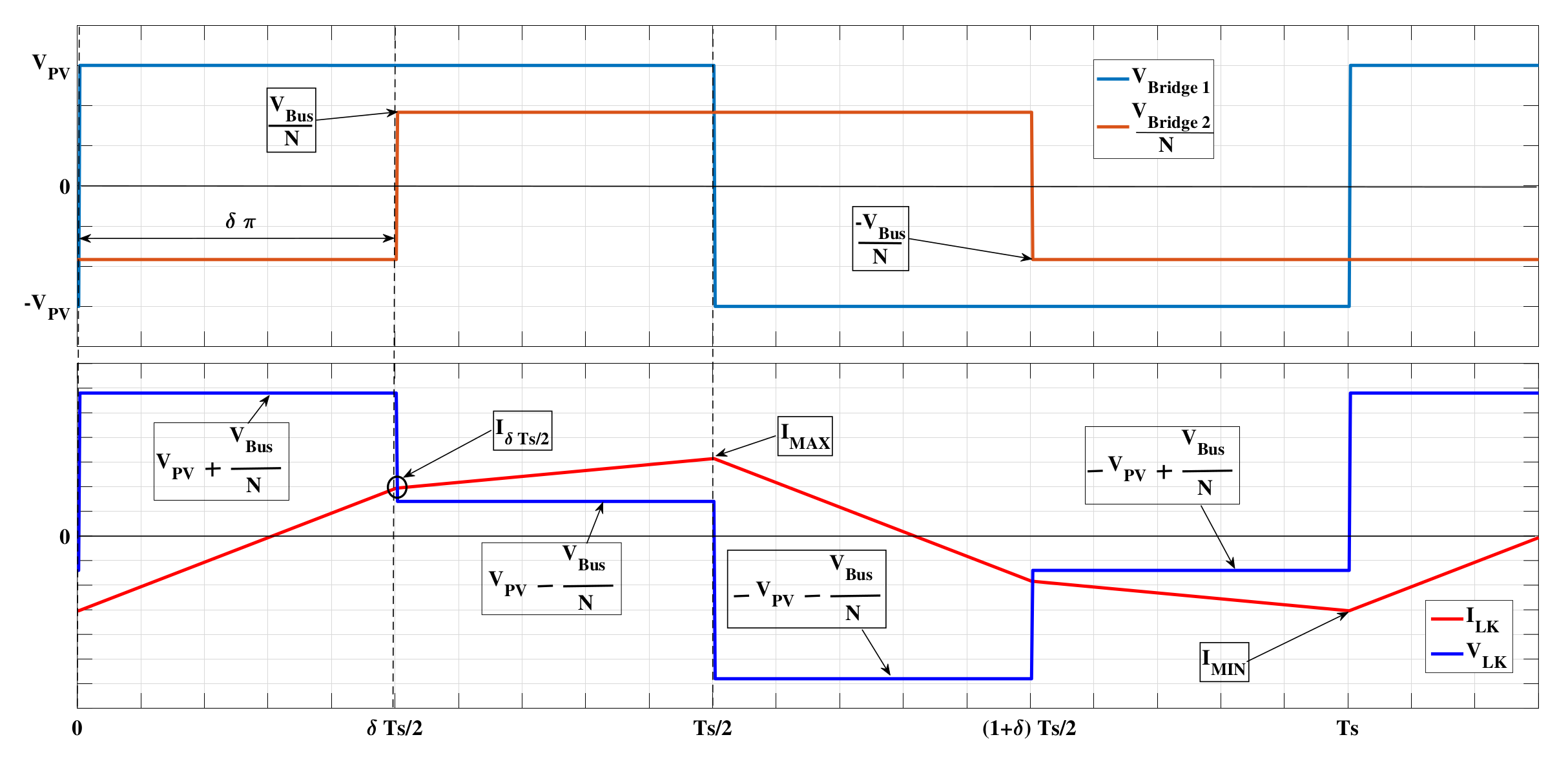
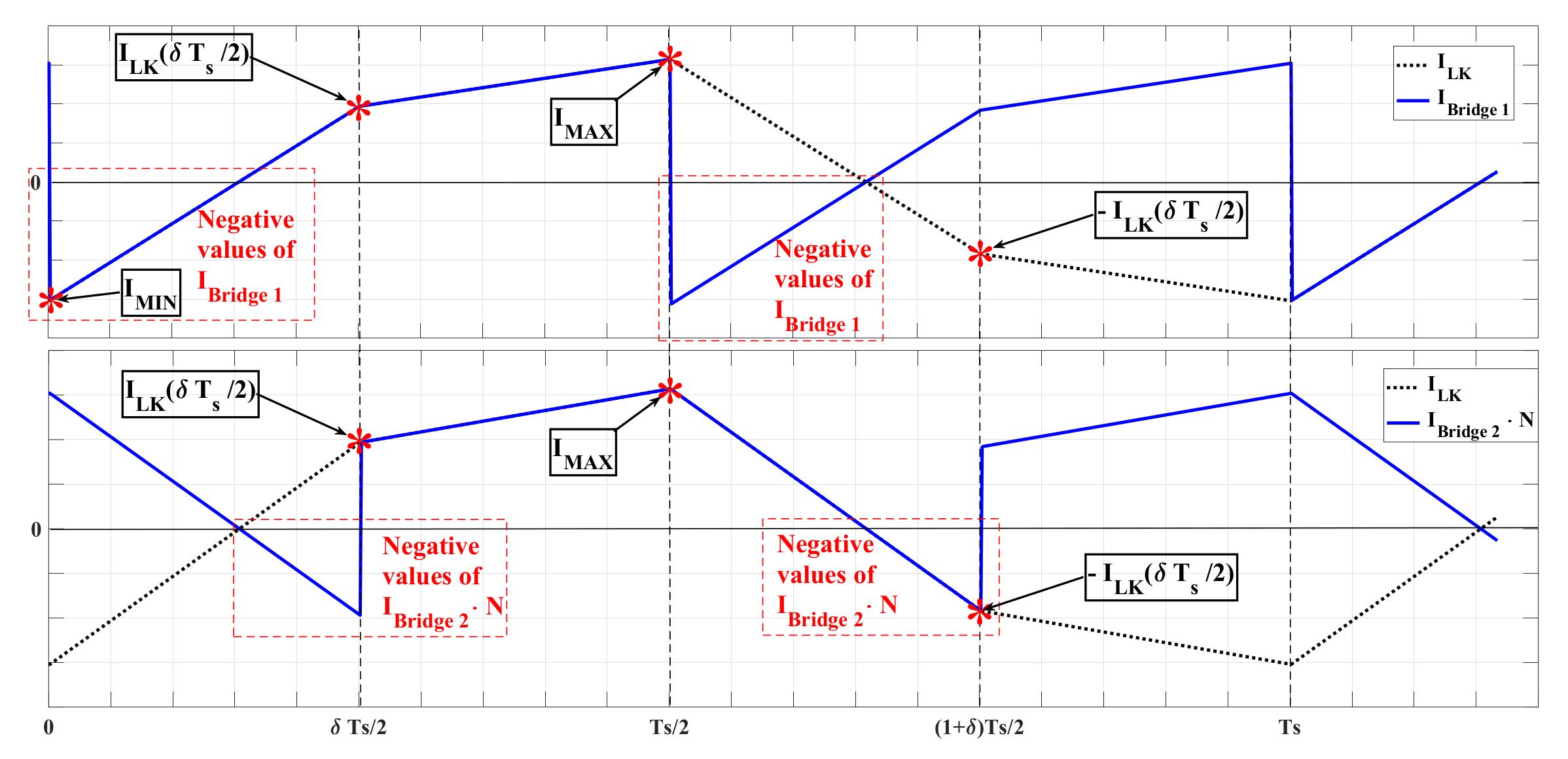
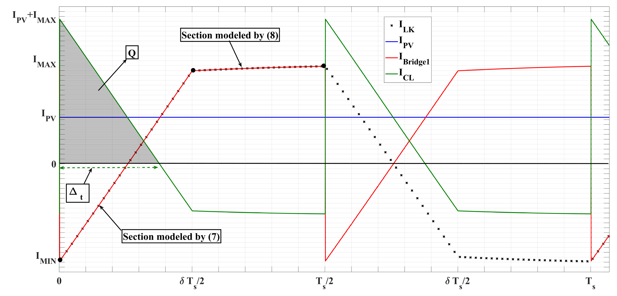
2.2.1. Leakage Inductor Current Analysis
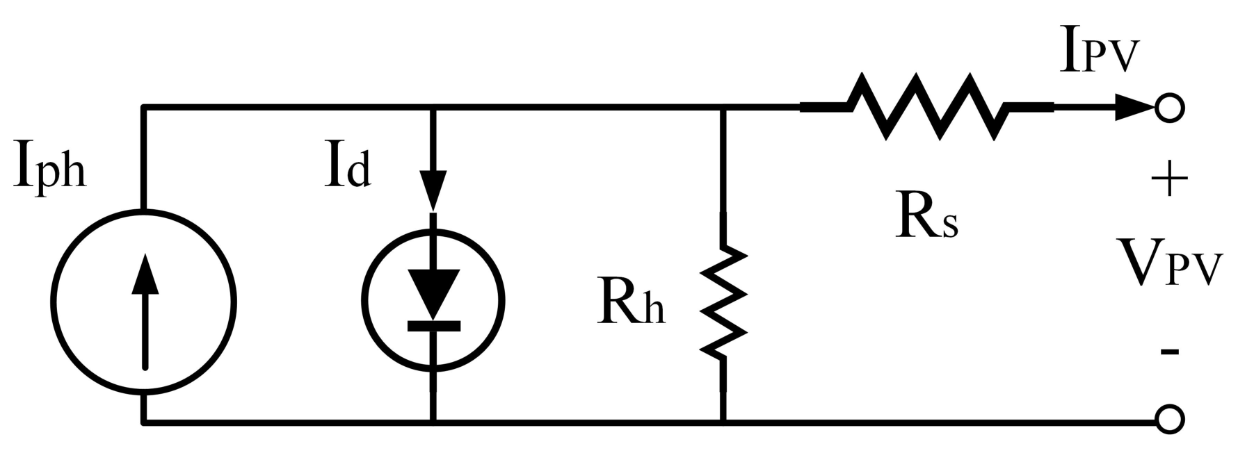
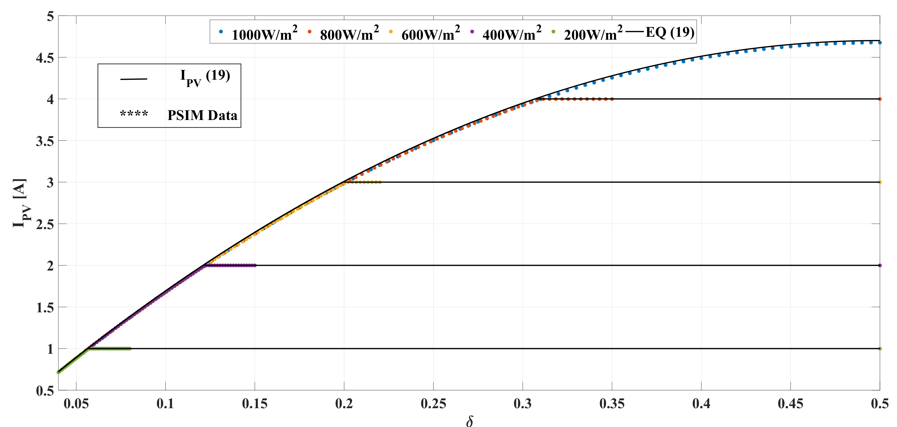
2.2.2. PV Current Analysis
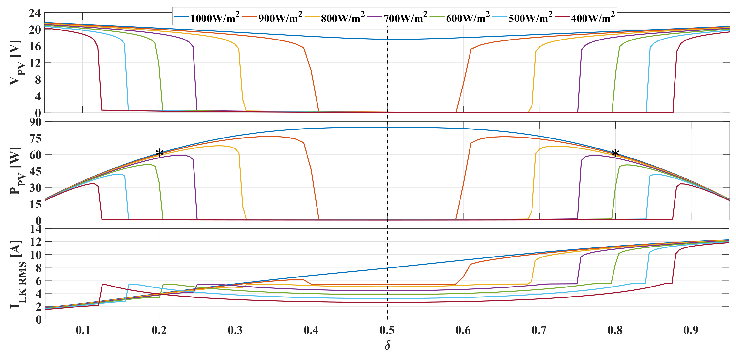
2.2.3. Range of Operation for the Phase Shift
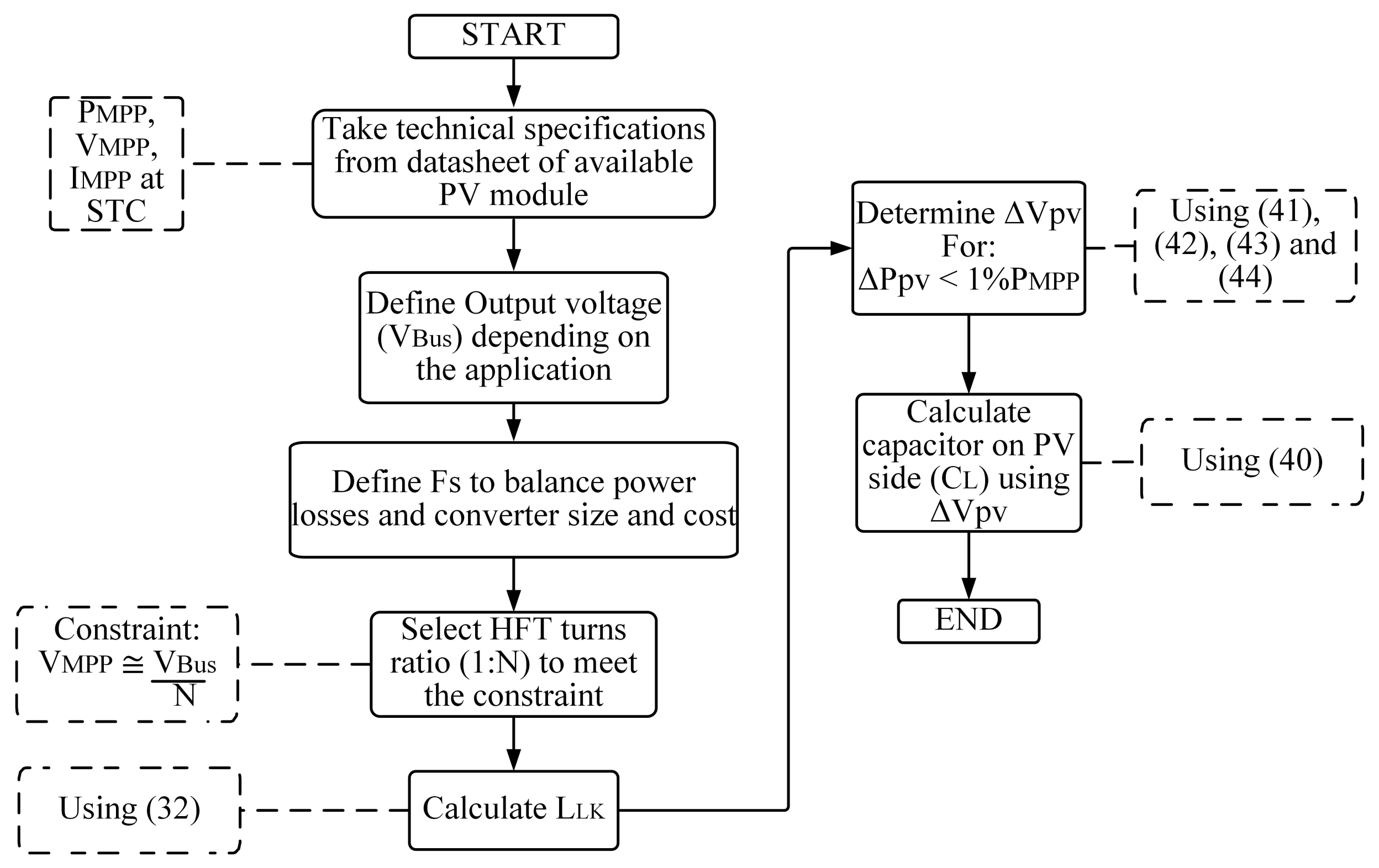
2.3. Design of the DAB Converter for PV Applications
2.3.1. Design of the HFT Equivalent Leakage Inductor
2.3.2. Design of the PV Side Capacitor
3. Results and Discussion
3.1. Design Example
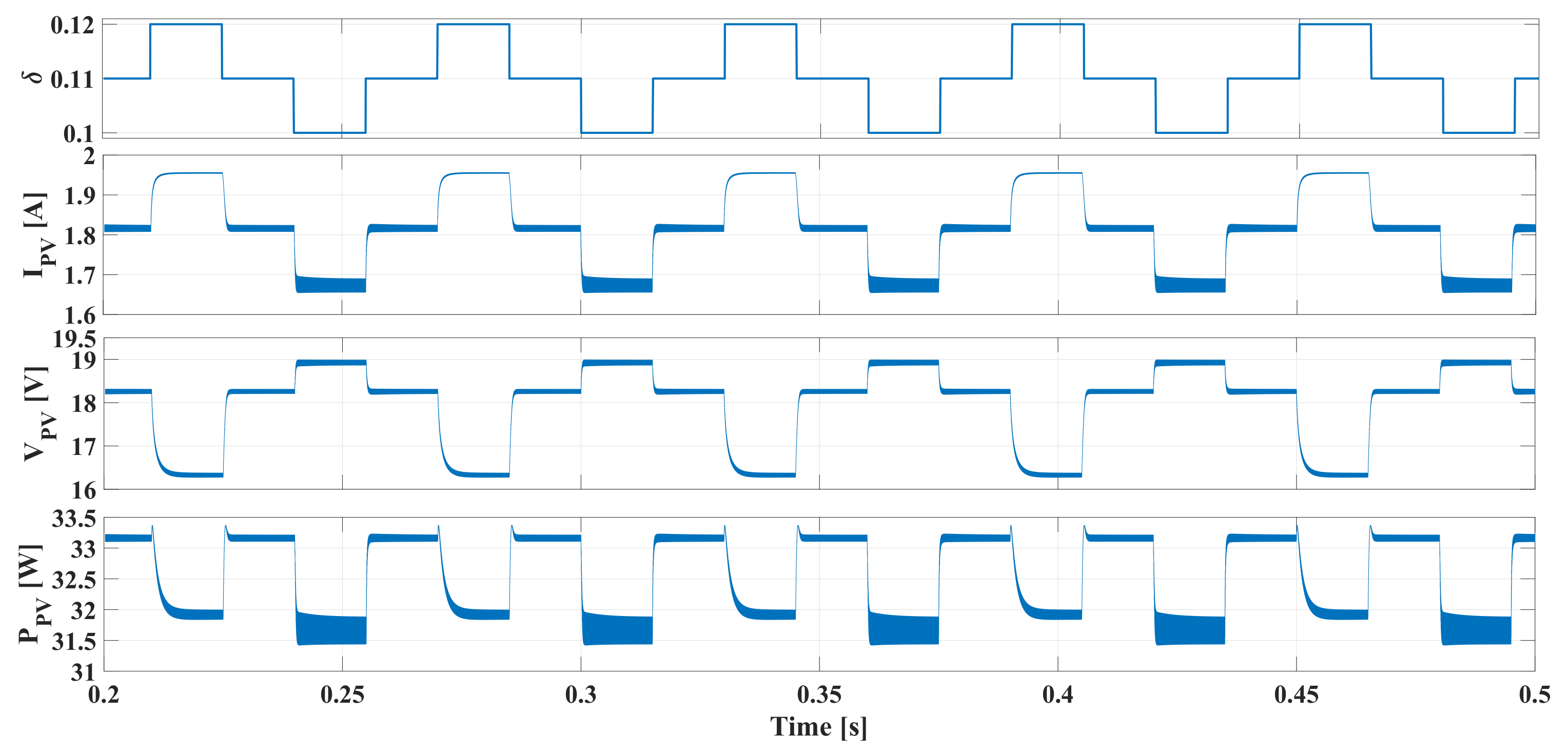
3.2. Verification of the Phase Shift () Optimal Range
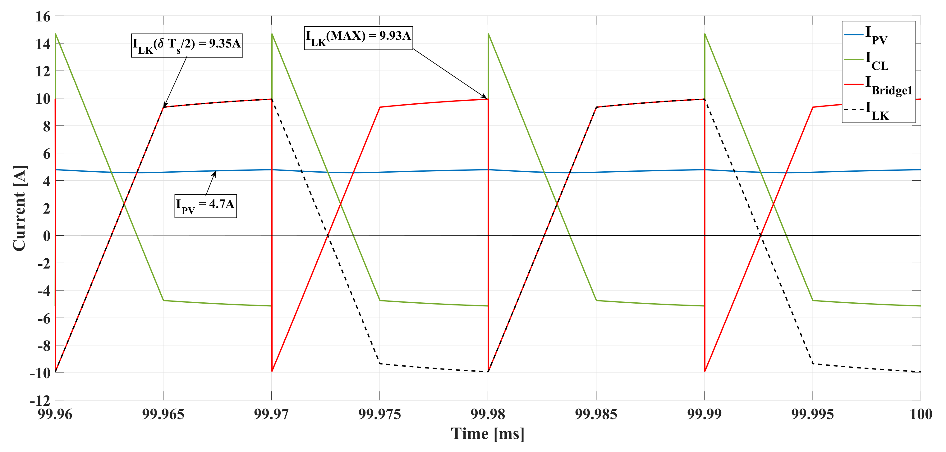
3.3. Verification of the PV Current Equation
3.4. Verification of the Design Equation
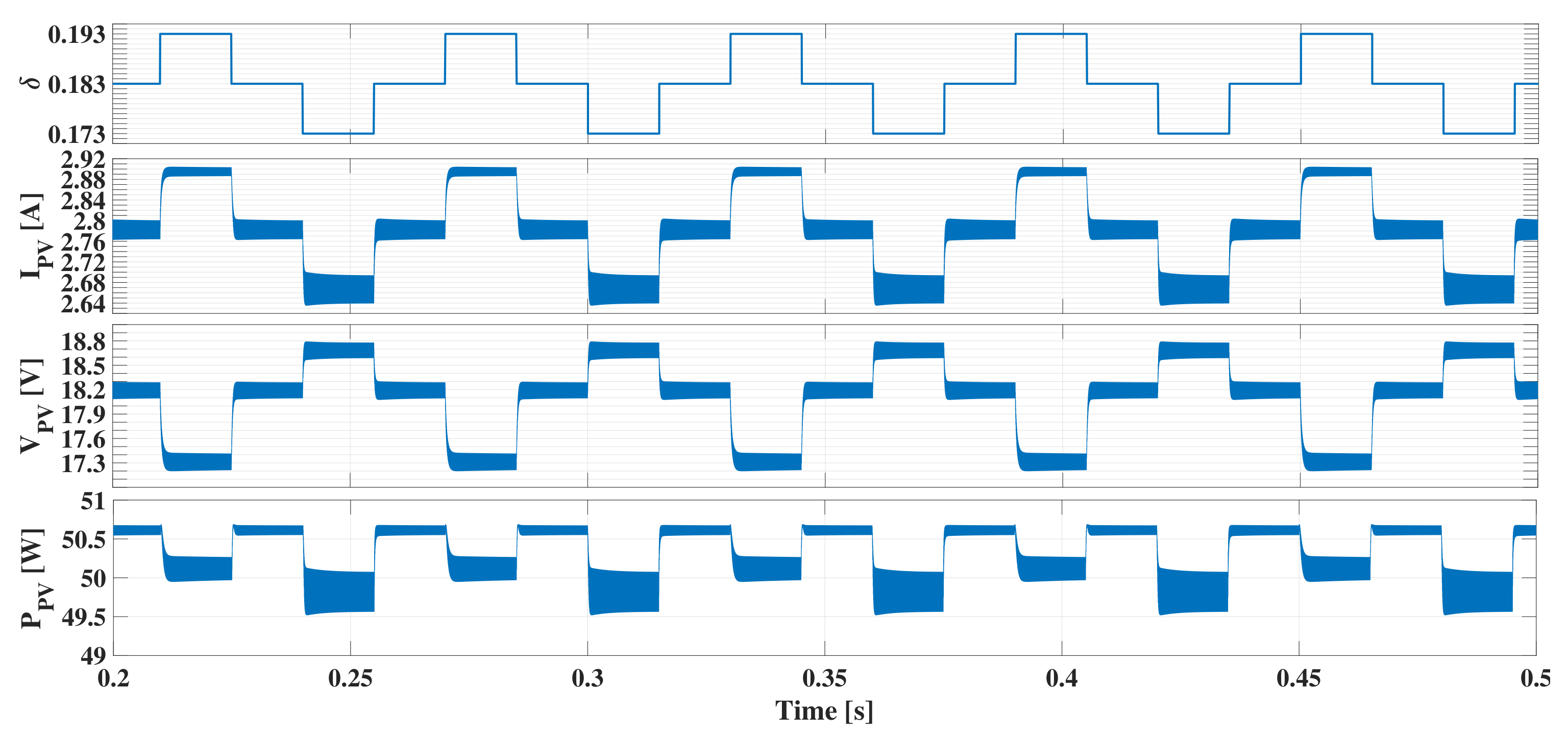
3.5. Verification of the Design Equation
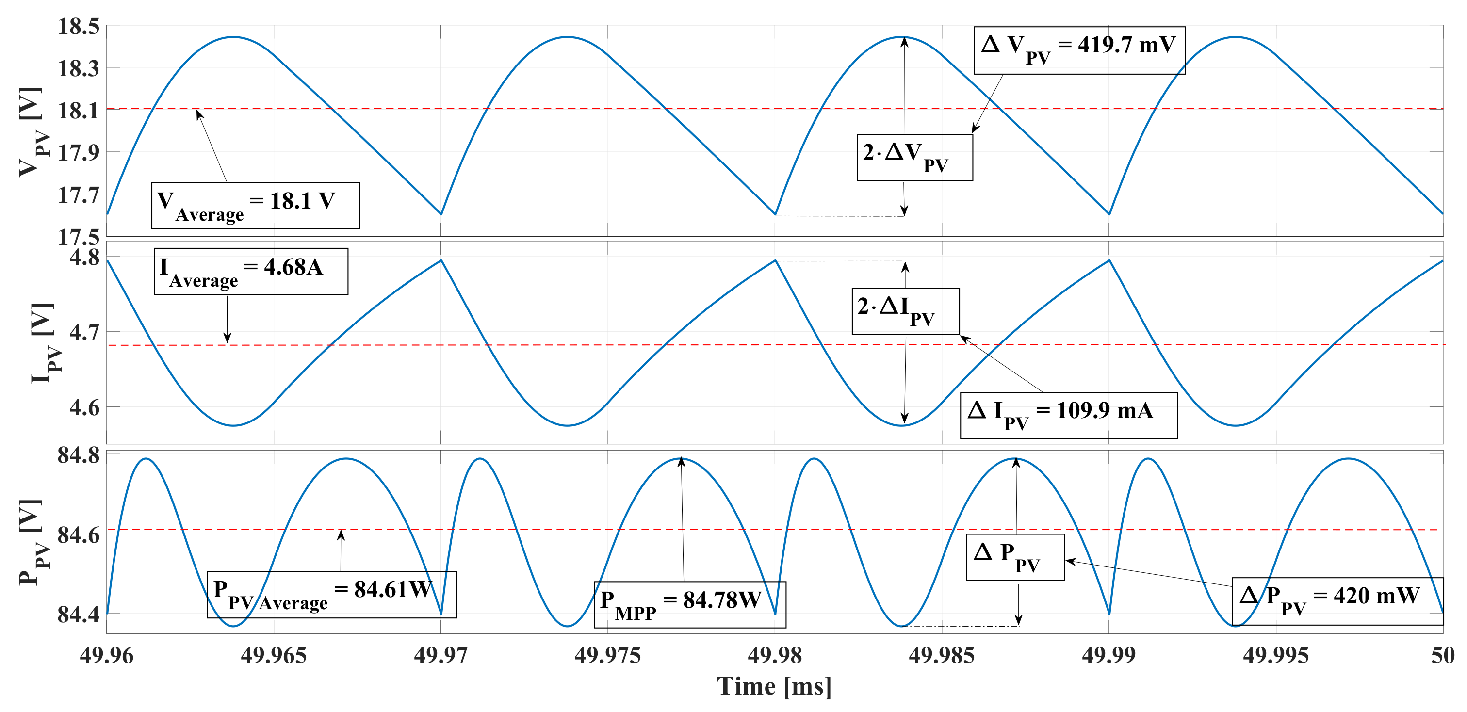
3.6. Verification of the Steady-State Operation
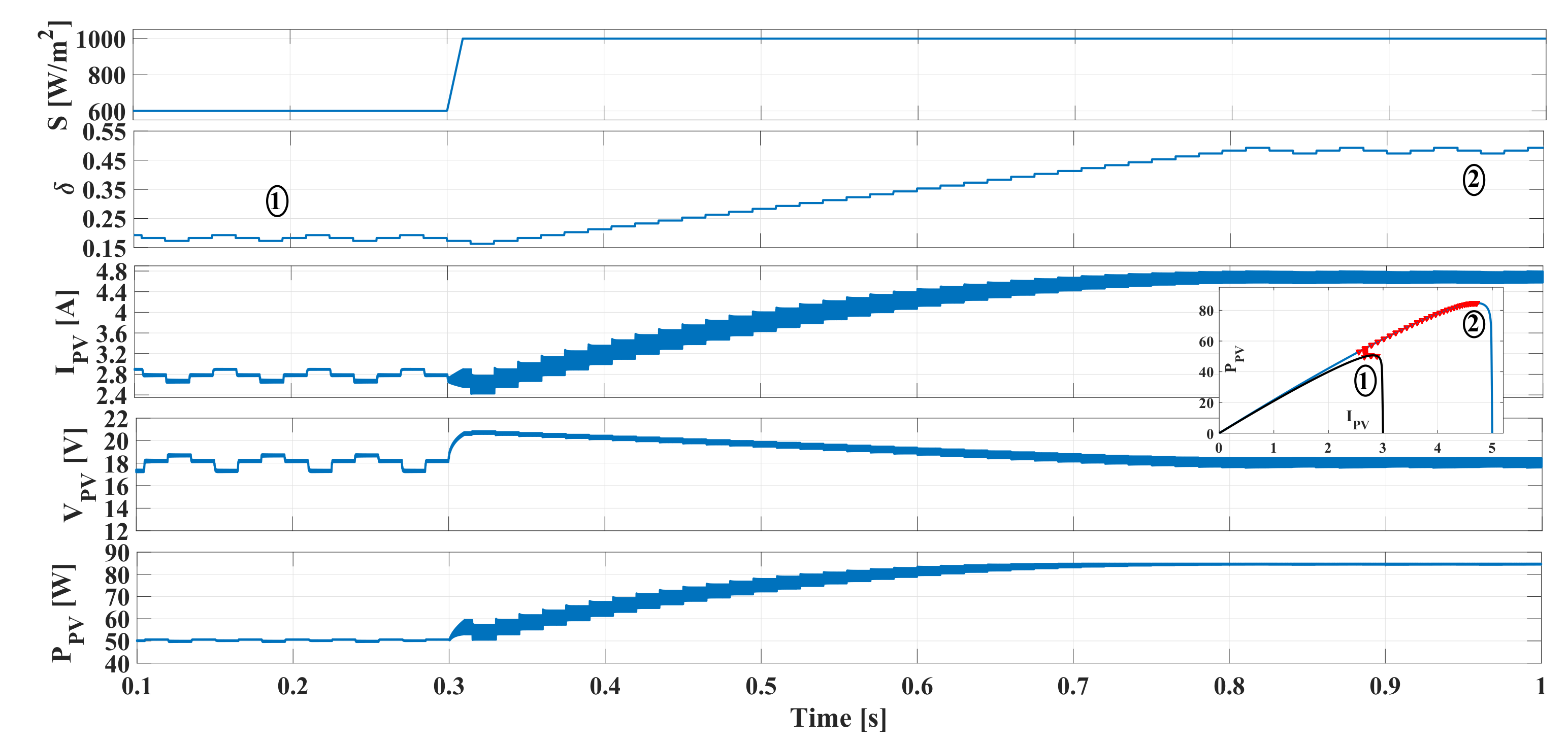
3.7. Verification of the Dynamic Operation with a MPPT Algorithm
4. Conclusions
Author Contributions
Funding
Conflicts of Interest
Abbreviations
| 1:N | HFT turns ratio |
| AC | Alternating current |
| ANN | Artificial neural network |
| Represents a power factor [W] | |
| Temperature coefficient of [%/C] | |
| Temperature coefficient of voltage [V/C] | |
| Phase shift angle between the diagonal switches on bridge 1 [Radians] | |
| B | Constant term of the linear equation [A] |
| BESS | Battery energy storage systems |
| Phase shift angle between the diagonal switches on bridge 2 [Radians] | |
| Output capacitor of the DAB converter [F] | |
| PV side capacitor of the DAB converter [F] | |
| CLK | Clock signal |
| D | Duty cycle |
| DAB | Dual active bridge |
| Output diode of the DAB converter | |
| DC | Direct current |
| DMPPT | distributed MPPT |
| DMMPT-U | DMPPT unit |
| Input diode of the DAB converter | |
| Phase shift factor | |
| Phase shift [Radians] | |
| step of the MPPT | |
| Ripple of the PV current [A] | |
| Ripple of the PV power [W] | |
| Time interval in which is positive [s] | |
| Ripple of the PV voltage [V] | |
| Switching frequency [Hz] | |
| HFT | High-frequency transformer |
| HVS | High-voltage side |
| Input current to bridge one [A] | |
| Output current from bridge two [A] | |
| Current in CL [A] | |
| Leakage inductor current [A] | |
| First straight-line section of [A] | |
| Second straight-line section of [A] | |
| RMS value of the leakage inductor current [A] | |
| Peak value on the positive section of [A] | |
| Peak value on the negative section of [A] | |
| PV current at MPP [A] | |
| Photo induced current of the single-diode model [A] | |
| PV current [A] | |
| Diode saturation current of the single-diode model [A] | |
| Short-circuit current of the PV module [A] | |
| Equivalent leakage inductance of HFT [H] | |
| Critical value [H] | |
| LVS | Low-voltage side |
| MPP | Maximum power point |
| MPPT | Maximum power point tracking |
| n | Harmonic number |
| Ideality factor of the single-diode model | |
| Active power on bridge one [W] | |
| Power delivered to the DC bus [W] | |
| Maximum power of the PV module [W] | |
| PV power at MPP [W] | |
| Fourier components of [W] | |
| Perturb-and-observe | |
| PV power [W] | |
| PSIM | Power electronics simulator |
| Instantaneous power flowing through [W] | |
| PV | Photovoltaic |
| PWM | Pulse-width modulation |
| Q | Electrical charge accumulated during the capacitor charging process [C] |
| HVS bridge (H), high transistor(H), leg one (1) | |
| HVS bridge (H), high transistor(H), leg two (2) | |
| HVS bridge (H), low transistor(L), leg one (1) | |
| HVS bridge (H), low transistor(L), leg two (2) | |
| LVS bridge (L), high transistor(H), leg one (1) | |
| LVS bridge (L), high transistor(H), leg two (2) | |
| LVS bridge (L), low transistor(L), leg one (1) | |
| LVS bridge (L), low transistor(L), leg two (2) | |
| Parallel resistance of the single-diode model | |
| Series resistance of the single-diode model | |
| S | Irradiation [W/m] |
| Switching function | |
| SPS | Single-phase shift |
| STC | Standard test conditions |
| t | Time [s] |
| Perturbation time of the MPPT algorithm [s] | |
| Switching period [s] | |
| PWM signal used to activate and | |
| Complementary PWM signal used to activate and | |
| PWM signal used to activate and | |
| Complementary PWM signal used to activate and | |
| Load voltage at HVS [V] | |
| Square voltage source [V], models the behavior of both PV module and bridge 1 | |
| Square voltage source [V], models the behavior of both DC bus and bridge 2 referred to the primary side | |
| Leakage inductor voltage [V] | |
| PV voltage at MPP [V] | |
| Open-Circuit voltage [V] | |
| PV voltage [V] | |
| VSI | Voltage source inverter |
| Thermal voltage of the PN junction in the PV cell [V] | |
| Lambert W function | |
| Angular switching frequency [Radians/s] | |
| X | Auxiliary variable to represent [V] |
| Y | Auxiliary variable to represent [V] |
| ZVS | Zero voltage switching |
References
- REN21. Renewables 2018 Global Status Report; Technical Report, Renewable Energy Policy Network for the 21st Century; REN21 Secretariat: Paris, France, 2018. [Google Scholar]
- Spagnuolo, G.; Kouro, S.; Vinnikov, D. Photovoltaic Module and Submodule Level Power Electronics and Control. IEEE Trans. Ind. Electron. 2019, 66, 3856–3859. [Google Scholar] [CrossRef]
- Romero-Cadaval, E.; Spagnuolo, G.; Franquelo, L.G.; Ramos-Paja, C.A.; Suntio, T.; Xiao, W.M. Grid-connected photovoltaic generation plants: Components and operation. IEEE Ind. Electron. Mag. 2013, 7, 6–20. [Google Scholar] [CrossRef] [Green Version]
- de Morais, J.C.d.S.; de Morais, J.L.d.S.; Gules, R. Photovoltaic AC Module Based on a Cuk Converter with a Switched-Inductor Structure. IEEE Trans. Ind. Electron. 2019, 66, 3881–3890. [Google Scholar] [CrossRef]
- Ardi, H.; Ajami, A.; Sabahi, M. A Novel High Step-Up DC–DC Converter with Continuous Input Current Integrating Coupled Inductor for Renewable Energy Applications. IEEE Trans. Ind. Electron. 2018, 65, 1306–1315. [Google Scholar] [CrossRef]
- Andrade, A.M.S.S.; Schuch, L.; da Silva Martins, M.L. Analysis and design of high-efficiency hybrid high step-Up DC-DC converter for distributed PV generation systems. IEEE Trans. Ind. Electron. 2019, 66, 3860–3868. [Google Scholar] [CrossRef]
- Messenger, R.A.; Ventre, J. Photovoltaic Systems Engineering, 2nd ed.; Taylor & Francis e-Library: Boca Raton, FL, USA, 2003; p. 480. [Google Scholar]
- Rajaei, A.; Khazan, R.; Mahmoudian, M.; Mardaneh, M.; Gitizadeh, M. A Dual Inductor High Step-Up DC/DC Converter Based on the Cockcroft–Walton Multiplier. IEEE Trans. Power Electron. 2018, 33, 9699–9709. [Google Scholar] [CrossRef]
- Velez-Sanchez, J.; Bastidas-Rodriguez, J.D.; Ramos-Paja, C.A.; Gonzalez-Montoya, D.; Trejos-Grisales, L.A. A Non-Invasive Procedure for Estimating the Exponential Model Parameters of Bypass Diodes in Photovoltaic Modules. Energies 2019, 12, 303. [Google Scholar] [CrossRef] [Green Version]
- Basoglu, M.E. An Improved 0.8 V OC Model Based GMPPT Technique for Module Level Photovoltaic Power Optimizers. IEEE Trans. Ind. Appl. 2019, 55, 1913–1921. [Google Scholar] [CrossRef]
- Hosseini, S.; Taheri, S.; Farzaneh, M.; Taheri, H. A High-Performance Shade-Tolerant MPPT Based on Current-Mode Control. IEEE Trans. Power Electron. 2019, 34, 10327–10340. [Google Scholar] [CrossRef]
- Bataineh, K. Improved hybrid algorithms-based MPPT algorithm for PV system operating under severe weather conditions. IET Power Electron. 2019, 12, 703–711. [Google Scholar] [CrossRef]
- Bastidas-Rodriguez, J.D.; Franco, E.; Petrone, G.; Ramos-Paja, C.A.; Spagnuolo, G. Maximum power point tracking architectures for photovoltaic systems in mismatching conditions: A review. IET Power Electron. 2014, 7, 1396–1413. [Google Scholar] [CrossRef]
- Vinnikov, D.; Chub, A.; Liivik, E.; Kosenko, R.; Korkh, O. Solar optiverter—A novel hybrid approach to the photovoltaic module level power electronics. IEEE Trans. Ind. Electron. 2019, 66, 3869–3880. [Google Scholar] [CrossRef]
- Huang, Q.; Huang, A.; Yu, R.; Liu, P.; Yu, W. High-Efficiency and High-Density Single-Phase Dual-Mode Cascaded Buck-Boost Multilevel Transformerless PV Inverter with GaN AC Switches. IEEE Trans. Power Electron. 2018, 34, 7474–7488. [Google Scholar] [CrossRef]
- Lee, H.S.; Yun, J.J. Quasi-Resonant Voltage Doubler with Snubber Capacitor for Boost Half-Bridge DC-DC Converter in Photovoltaic Micro-Inverter. IEEE Trans. Power Electron. 2018, 34, 8377–8388. [Google Scholar] [CrossRef]
- Roy, J.; Xia, Y.; Ayyanar, R. High Step-Up Transformerless Inverter for AC Module Applications with Active Power Decoupling. IEEE Trans. Ind. Electron. 2019, 66, 3891–3901. [Google Scholar] [CrossRef]
- Mohan, N.; Undeland, T.M.; Robbins, W.P. Power Electronics. Converters, Applications and Design, 3rd ed.; John Wiley and Sons, Inc.: Hoboken, NJ, USA, 2002; p. 824. [Google Scholar]
- Ravishankar, J.; Binu Ben Jose, D.; Ammasai Gounden, N. Simple power electronic controller for photovoltaic fed grid-tied systems using line commutated inverter with fixed firing angle. IET Power Electron. 2014, 7, 1424–1434. [Google Scholar] [CrossRef]
- Li, K.; Hu, Y.; Ioinovici, A. Generation of the Large DC Gain Step-Up Nonisolated Converters in Conjunction With Renewable Energy Sources Starting From a Proposed Geometric Structure. IEEE Trans. Power Electron. 2017, 32, 5323–5340. [Google Scholar] [CrossRef]
- Surapaneni, R.K.; Das, P. A Z-Source-Derived Coupled-Inductor-Based High Voltage Gain Microinverter. IEEE Trans. Ind. Electron. 2018, 65, 5114–5124. [Google Scholar] [CrossRef]
- Gautam, V.; Sensarma, P. Design of Ćuk-Derived Transformerless Common-Grounded PV Microinverter in CCM. IEEE Trans. Ind. Electron. 2017, 64, 6245–6254. [Google Scholar] [CrossRef]
- Kan, J.; Wu, Y.; Tang, Y.; Xie, S.; Jiang, L. Hybrid Control Scheme for Photovoltaic Micro-Inverter with Adaptive Inductor. IEEE Trans. Power Electron. 2018, 34, 8762–8774. [Google Scholar] [CrossRef]
- Sukesh, N.; Pahlevaninezhad, M.; Jain, P.K. Analysis and Implementation of a Single-Stage Flyback PV Microinverter With Soft Switching. IEEE Trans. Ind. Electron. 2014, 61, 1819–1833. [Google Scholar] [CrossRef]
- Surapaneni, R.K.; Rathore, A.K. A Single-Stage CCM Zeta Microinverter for Solar Photovoltaic AC Module. IEEE J. Emerg. Sel. Top. Power Electron. 2015, 3, 892–900. [Google Scholar] [CrossRef]
- Meneses, D.; Garcia, O.; Alou, P.; Oliver, J.A.; Cobos, J.A. Grid-Connected Forward Microinverter With Primary-Parallel Secondary-Series Transformer. IEEE Trans. Power Electron. 2015, 30, 4819–4830. [Google Scholar] [CrossRef] [Green Version]
- Lee, S.H.; Cha, W.J.; Kwon, J.M.; Kwon, B.H. Control Strategy of Flyback Microinverter With Hybrid Mode for PV AC Modules. IEEE Trans. Ind. Electron. 2016, 63, 995–1002. [Google Scholar] [CrossRef]
- Lee, S.H.; Cha, W.J.; Kwon, B.H.; Kim, M. Discrete-Time Repetitive Control of Flyback CCM Inverter for PV Power Applications. IEEE Trans. Ind. Electron. 2016, 63, 976–984. [Google Scholar] [CrossRef]
- Chub, A.; Vinnikov, D.; Blaabjerg, F.; Peng, F.Z. A review of galvanically isolated impedance-source DC-DC converters. IEEE Trans. Power Electron. 2016. [Google Scholar] [CrossRef]
- Junior, L.G.; De Brito, M.A.; Sampaio, L.P.; Canesin, C.A. Single stage converters for low power stand-alone and grid-connected PV systems. In Proceedings of the ISIE 2011: 2011 IEEE International Symposium on Industrial Electronics, Gdansk, Poland, 27–30 June 2011; pp. 1112–1117. [Google Scholar] [CrossRef]
- Zhao, B.; Song, Q.; Liu, W.; Sun, Y. Overview of dual-active-bridge isolated bidirectional DC-DC converter for high-frequency-link power-conversion system. IEEE Trans. Power Electron. 2014, 29, 4091–4106. [Google Scholar] [CrossRef]
- Yazdani, F.; Zolghadri, M. Design of dual active bridge isolated bi-directional DC converter based on current stress optimization. In Proceedings of the 2017 8th Power Electronics, Drive Systems & Technologies Conference (PEDSTC), Mashhad, Iran, 14–16 February 2017; pp. 247–252. [Google Scholar] [CrossRef]
- Segaran, D.S. Dynamic Modelling and Control of Dual Active Bridge Bi-directional DC-DC Converters for Smart Grid Applications. Ph.D. Thesis, Royal Melbourne Institute of Technology University, Melbourne, VIC, Australia, 2013. [Google Scholar]
- Jeung, Y.C.; Lee, D.C. Voltage and current regulations of bidirectional isolated dual-active-bridge DC-DC converters based on a double-integral sliding mode control. IEEE Trans. Power Electron. 2019, 34, 6937–6946. [Google Scholar] [CrossRef]
- Wang, D.; Nahid-Mobarakeh, B.; Emadi, A. Second Harmonic Current Reduction for a Battery-Driven Grid Interface With Three-Phase Dual Active Bridge DC–DC Converter. IEEE Trans. Ind. Electron. 2019, 66, 9056–9064. [Google Scholar] [CrossRef]
- Bayat, H.; Yazdani, A. A Hybrid MMC-Based Photovoltaic and Battery Energy Storage System. IEEE Power Energy Technol. Syst. J. 2019, 6, 32–40. [Google Scholar] [CrossRef]
- Gonzalez-Agudelo, D.; Escobar-Mejia, A.; Ramirez-Murrillo, H. Dynamic model of a dual active bridge suitable for solid state transformers. In Proceedings of the International Power Electronics Congress—CIEP, Guanajuato, Mexico, 20–23 June 2016; pp. 350–355. [Google Scholar] [CrossRef]
- Agrawal, A.; Nalamati, C.S.; Gupta, R. Hybrid DC–AC Zonal Microgrid Enabled by Solid-State Transformer and Centralized ESD Integration. IEEE Trans. Ind. Electron. 2019, 66, 9097–9107. [Google Scholar] [CrossRef]
- Parreiras, T.M.; MacHado, A.P.; Amaral, F.V.; Lobato, G.C.; Brito, J.A.; Filho, B.C. Forward Dual-Active-Bridge Solid-State Transformer for a SiC-Based Cascaded Multilevel Converter Cell in Solar Applications. IEEE Trans. Ind. Appl. 2018, 54, 6353–6363. [Google Scholar] [CrossRef]
- Mansour, A.; Faouzi, B.; Jamel, G.; Ismahen, E. Design and analysis of a high frequency DC–DC converters for fuel cell and super-capacitor used in electrical vehicle. Int. J. Hydrogen Energy 2014, 39, 1580–1592. [Google Scholar] [CrossRef]
- Marei, M.I.; El-Helw, H.; Al-Hasheem, M. A grid-connected PV interface system based on the DAB-converter. In Proceedings of the 2015 IEEE 15th International Conference on Environment and Electrical Engineering (EEEIC), Rome, Italy, 10–13 June 2015; pp. 161–165. [Google Scholar] [CrossRef]
- El-Helw, H.M.; Al-Hasheem, M.; Marei, M.I. Control strategies for the DAB based PV interface system. PLoS ONE 2016, 11, e0161856. [Google Scholar] [CrossRef] [PubMed]
- Hu, J.; Joebges, P.; Pasupuleti, G.C.; Averous, N.R.; De Doncker, R.W. A Maximum-Output-Power-Point-Tracking Controlled Dual-Active Bridge Converter for Photovoltaic Energy Integration into MVDC Grids. IEEE Trans. Energy Convers. 2018, 34, 170–180. [Google Scholar] [CrossRef]
- Shi, Y.; Li, R.; Xue, Y.; Li, H. High-frequency-link-based grid-tied PV system with small DC-link capacitor and low-frequency ripple-free maximum power point tracking. IEEE Trans. Power Electron. 2016, 31, 328–339. [Google Scholar] [CrossRef]
- Liu, T.; Yang, X.; Chen, W.; Li, Y.; Xuan, Y.; Huang, L.; Hao, X. Design and Implementation of High Efficiency Control Scheme of Dual Active Bridge Based 10 kV/1 MW Solid State Transformer for PV Application. IEEE Trans. Power Electron. 2019, 34, 4223–4238. [Google Scholar] [CrossRef]
- Xu, G.; Sha, D.; Xu, Y.; Liao, X. Dual-Transformer-Based DAB Converter with Wide ZVS Range for Wide Voltage Conversion Gain Application. IEEE Trans. Ind. Electron. 2018, 65, 3306–3316. [Google Scholar] [CrossRef]
- Wang, H.; Wei, T.; Sun, X.; Wan, X.; Wang, F.; Zhuo, F. The application of cascade power electronic transformer in large-scale photovoltaic power generation system. In Proceedings of the PEDG 2019—2019 IEEE 10th International Symposium on Power Electronics for Distributed Generation Systems, Xi’an, China, 3–6 June 2019; Institute of Electrical and Electronics Engineers Inc.: Xi’an, China, 2019; pp. 425–428. [Google Scholar] [CrossRef]
- Aguirre, M.; Yazdani, A. A single-phase dc-ac dual-active-bridge based resonant converter for grid-connected Photovoltaic (PV) applications. In Proceedings of the 2019 21st European Conference on Power Electronics and Applications, EPE 2019 ECCE Europe, Genova, Italy, 3–5 September 2019; Institute of Electrical and Electronics Engineers Inc.: Genova, Italy, 2019. [Google Scholar] [CrossRef]
- Rodriguez, A.; Vazquez, A.; Lamar, D.G.; Hernando, M.M.; Sebastian, J. Different purpose design strategies and techniques to improve the performance of a Dual Active Bridge with phase-shift control. IEEE Trans. Power Electron. 2015, 30, 790–804. [Google Scholar] [CrossRef]
- Kim, K.S.; Jeong, S.G.; Kwon, B.H. Single power-conversion DAB microinverter with safe commutation and high efficiency for PV power applications. Sol. Energy 2019, 193, 676–683. [Google Scholar] [CrossRef]
- Zhao, B.; Song, Q.; Liu, W.; Liu, G.; Zhao, Y. Universal High-Frequency-Link Characterization and Practical Fundamental-Optimal Strategy for Dual-Active-Bridge DC-DC Converter under PWM Plus Phase-Shift Control. IEEE Trans. Power Electron. 2015, 30, 6488–6494. [Google Scholar] [CrossRef]
- Erickson, R.W.; Maksimovic, D.; Erickson, R.W.; Maksimovic, D. Fundamentals of Power Electronics, 2nd ed.; Springer: New York, NY, USA, 2005; p. 883. [Google Scholar]
- Ferreira, C.; Lopez, J.L. Asymptotic expansions of the Hurwitz–Lerch zeta function. J. Math. Anal. Appl. 2004, 298, 210–224. [Google Scholar] [CrossRef]
- Petrone, G.; Ramos-Paja, C.A.; Spagnuolo, G. Photovoltaic Sources Modeling, 1st ed.; Wiley: Pondicherry, India, 2017; Volume 1, p. 196. [Google Scholar]
- Femia, N.; Petrone, G.; Spagnuolo, G.; Vitelli, M. Optimization of perturb and observe maximum power point tracking method. IEEE Trans. Power Electron. 2005, 20, 963–973. [Google Scholar] [CrossRef]
- Ahmed, J.; Salam, Z. An improved perturb and observe (P&O) maximum power point tracking (MPPT) algorithm for higher efficiency. Appl. Energy 2015, 150, 97–108. [Google Scholar] [CrossRef]
- Mamarelis, E.; Petrone, G.; Spagnuolo, G. A two-steps algorithm improving the P&O steady state MPPT efficiency. Appl. Energy 2014, 113, 414–421. [Google Scholar] [CrossRef]
- Valentini, M.; Raducu, A.; Sera, D.; Teodorescu, R. PV inverter test setup for european efficiency, static and dynamic MPPT efficiency evaluation. In Proceedings of the 11th International Conference on Optimization of Electrical and Electronic Equipment, OPTIM 2008, Brasov, Romania, 22–24 May 2008; IEEE: Piscataway, NJ, USA, 2008; pp. 433–438. [Google Scholar] [CrossRef]
- Sera, D.; Kerekes, T.; Teodorescu, R.; Blaabjerg, F. Improved MPPT Algorithms for Rapidly Changing Environmental Conditions. In Proceedings of the 12th International Power Electronics and Motion Control Conference, Portoroz, Slovenia, 30 August–1 September 2006; IEEE: Piscataway, NJ, USA, 2006; pp. 1614–1619. [Google Scholar] [CrossRef]
- BP Solar. BP585 Solar Modules; BP Solar: Madrid, Spain, 2003. [Google Scholar]
- Accarino, J.; Petrone, G.; Ramos-Paja, C.A.; Spagnuolo, G. Symbolic algebra for the calculation of the series and parallel resistances in PV module model. In Proceedings of the 4th International Conference on Clean Electrical Power: Renewable Energy Resources Impact (ICCEP 2013), Alghero, Italy, 11–13 June 2013; pp. 62–66. [Google Scholar] [CrossRef]
- de Souza, I.D.; de Almeida, P.M.; Barbosa, P.G.; Duque, C.A.; Ribeiro, P.F. Digital single voltage loop control of a VSI with LC output filter. Sustain. Energy Grids Netw. 2018, 16, 145–155. [Google Scholar] [CrossRef]
- Sechilariu, M.; Wang, B.; Locment, F. Building-integrated microgrid: Advanced local energy management for forthcoming smart power grid communication. Energy Build. 2013, 59, 236–243. [Google Scholar] [CrossRef]
- Ting, Y.; de Haan, S.; Ferreira, J.A. Elimination of switching losses in the single active bridge over a wide voltage and load range at constant frequency. In Proceedings of the 2013 15th European Conference on Power Electronics and Applications (EPE), Lille, France, 2–6 September 2013; pp. 1–10. [Google Scholar] [CrossRef]
- Liu, F.; Sun, X.; Feng, J.; Wu, J.; Li, X. The improved dual active bridge converter with a modified phase shift and variable frequency control. In Proceedings of the 2018 IEEE Applied Power Electronics Conference and Exposition (APEC), San Antonio, TX, USA, 4–8 March 2018; pp. 814–819. [Google Scholar] [CrossRef]
- Li, J.; Chen, Z.; Shen, Z.; Mattavelli, P.; Liu, J.; Boroyevich, D. An adaptive dead-time control scheme for high-switching-frequency dual-active-bridge converter. In Proceedings of the 2012 Twenty-Seventh Annual IEEE Applied Power Electronics Conference and Exposition (APEC), Orlando, FL, USA, 5–9 February 2012; pp. 1355–1361. [Google Scholar] [CrossRef]
- Han, X.; Tan, Y.; Ma, H. The switching frequency optimization of dual phase shift control for dual active bridge DC-DC converter. In Proceedings of the IECON 2017—43rd Annual Conference of the IEEE Industrial Electronics Society, Beijing, China, 29 October–1 November 2017; pp. 1610–1615. [Google Scholar] [CrossRef]
- Aganza-Torres, A.; Cárdenas, V.; Pacas, M. Generalized average model for a high-frequency link grid-connected DC/AC converter. Int. J. Electr. Power Energy Syst. 2019, 107, 344–351. [Google Scholar] [CrossRef]
- Evangelou, S.A.; Rehman-Shaikh, M. Hybrid electric vehicle fuel minimization by DC-DC converter dual-phase-shift control. Control Eng. Pract. 2017, 64, 44–60. [Google Scholar] [CrossRef]
- Monika, M.; Rane, M.; Wagh, S.; Stanković, A.; Singh, N. Development of dynamic phasor based higher index model for performance enhancement of dual active bridge. Electr. Power Syst. Res. 2019, 168, 305–312. [Google Scholar] [CrossRef]
- Li, J.; Wang, D.; Wang, W.; Jiang, J. Minimize Current Stress of Dual-Active-Bridge DC-DC Converters for Electric Vehicles Based on Lagrange Multipliers Method. Energy Procedia 2017, 105, 2733–2738. [Google Scholar] [CrossRef]
- Nguyen, D.D.; Nguyen, D.H.; Ta, M.C.; Fujita, G. Sensorless Feedforward Current Control of Dual-Active-Bridge DC/DC Converter for Micro-Grid Applications. IFAC-PapersOnLine 2018, 51, 333–338. [Google Scholar] [CrossRef]


| Solar Panel Parameters at STC | ||
|---|---|---|
| Maximum power | 85 W | |
| Voltage at Pmax | 18 V | |
| Current at Pmax | 4.72 A | |
| Short-circuit current | 5 A | |
| Open-Circuit voltage | 22.1 V | |
| Temperature coefficient of | 0.065 %/C | |
| Temperature coefficient of voltage | −80 mV/C | |
| DAB Converter parameters | ||
| Input capacitor | 33 F | |
| Output capacitor | 88 F | |
| Leakage inductor | 9 H | |
| Transformer turns ratio | ||
| Switching Frequency | 50 kHz | |
| DC BUS parameters | ||
| DC Bus voltage | 220 V | |
© 2020 by the authors. Licensee MDPI, Basel, Switzerland. This article is an open access article distributed under the terms and conditions of the Creative Commons Attribution (CC BY) license (http://creativecommons.org/licenses/by/4.0/).
Share and Cite
Henao-Bravo, E.E.; Ramos-Paja, C.A.; Saavedra-Montes, A.J.; González-Montoya, D.; Sierra-Pérez, J. Design Method of Dual Active Bridge Converters for Photovoltaic Systems with High Voltage Gain. Energies 2020, 13, 1711. https://doi.org/10.3390/en13071711
Henao-Bravo EE, Ramos-Paja CA, Saavedra-Montes AJ, González-Montoya D, Sierra-Pérez J. Design Method of Dual Active Bridge Converters for Photovoltaic Systems with High Voltage Gain. Energies. 2020; 13(7):1711. https://doi.org/10.3390/en13071711
Chicago/Turabian StyleHenao-Bravo, Elkin Edilberto, Carlos Andrés Ramos-Paja, Andrés Julián Saavedra-Montes, Daniel González-Montoya, and Julián Sierra-Pérez. 2020. "Design Method of Dual Active Bridge Converters for Photovoltaic Systems with High Voltage Gain" Energies 13, no. 7: 1711. https://doi.org/10.3390/en13071711