Article

Design and Implementation a Single-Switch Step-Up DC-DC Converter Based on Cascaded Boost and Luo Converters

by
Hossein Gholizadeh
1,
Reza Sharifi Shahrivar
2,
Mir Reza Hashemi
1,
Ebrahim Afjei
1 and
Saman A. Gorji
3,4,*
1
Faculty of Electrical Engineering, Shahid Beheshti University, Tehran 25529, Iran
2
Faculty of Electrical Engineering, Islamic Azad University, Tehran 25529, Iran
3
Science and Engineering Faculty, Queensland University of Technology, Brisbane 4001, Australia
4
Centre for Clean Energy Technologies and Practices, Queensland University of Technology, Brisbane 4001, Australia
*
Author to whom correspondence should be addressed.
Energies 2021, 14(12), 3584; https://doi.org/10.3390/en14123584
Submission received: 12 May 2021 / Revised: 8 June 2021 / Accepted: 12 June 2021 / Published: 16 June 2021

Abstract

:
We designed and implemented a single-switch step-up DC-DC converter based on cascaded boost and Luo converters. The proposed converter demonstrated a quadratic voltage gain and a high efficiency, which makes it suitable for renewable energy applications, where a high voltage gain ratio is desired without imposing a high number of bulky items or employing a high duty cycle of the active switches. This converter benefits from the continuity of the input current waveform, which equips the maximum utilisation of renewable energy sources. While a transformer-less high voltage-gain was achieved, the voltage and current stresses of the power switch and diodes were kept low in comparison with the existing quadratic DC-DC converters. We analysed the converter in both continuous and discontinuous conduction modes. A non-ideal model of components was considered for power loss and efficiency calculations and comparisons. Finally, the simulation results were extracted with PLECS and validated with experiments on a 120 W prototype.

1. Introduction

The DC-DC topologies can be mainly divided into isolated and non-isolated designs. The turn ratio of the coils in the isolated topologies acts an essential role in the increase of the voltage gain, independent of the high value of the duty cycle. The isolation that takes place by the existence of the high-frequency transformer protects the sensitive loads against the faults of the input source. Despite the aforementioned advantages, the increased volume, weight, price, and loss are the drawbacks of adding a magnetic core. Moreover, the discontinuity of the input current and the leakage inductors indicates the employment of snubber circuits, which increase the number of circuit components and complexity of the converter.
Therefore, it is a reasonable choice to utilise a non-isolated topology when there is no great rationale to apply an isolated circuit. Among the canonical non-isolated converters, including buck, buck-boost, and boost converters, the buck-boost and boost converters can step up the voltage level of the input source. The discontinuous input and output currents as well as the negative polarity of the output voltage are the main disadvantages of buck-boost converters. The storage of the energy in the inductor during the first mode and the subsequent release of that energy to the load makes the 50 percent duty cycle the best choice. Consequently, such a situation causes a pass-through rather than a step-up in the buck-boost converter [1,2,3].
The conventional boost converter can step up the input voltage gain. Theoretically, by increasing the duty cycle and its approach to unity, higher orders of voltage gain can be achieved. However, the practical results are not compatible with the theoretical relations [1,2,3]. The approach of the duty cycle to unity makes the conduction time of the diode approach zero, which complicates the the reverse recovery time of the diodes. The higher value of the duty-cycle yields a higher voltage/current stress of switches and diodes, which leads to higher losses [4,5,6,7,8].
The mentioned concepts make the fields ready for the emergence of the new topologies of the DC-DC converters. One of the offered structures is the cascade of the boost converter, which is illustrated in Figure 1a. As can be understood, a switch and three diodes were employed in its topology, which was obtained by the connection of two boost topologies. When the duty cycle becomes 50 percent, the voltage gain becomes four. In other words, the behaviour is same as the suggested topology in [9].
To achieve higher values of the voltage gain, the duty-cycle has to approach unity, which can significantly decrease the efficiency due to the increase in the number of the components. The other high step-up topology is a Luo converter, which is illustrated in Figure 1b. In comparison with the boost topology, the current ripple of the input current is higher, which increases the value of the input DC-link capacitor. In other words, during the first operation mode of the stated converter, the first diode becomes ON as the switch becomes activated. The mentioned diode is activated due to the current made via the parallel connection of the first capacitor and the input source.
Such a current does not appear in the second mode. Therefore, the input current ripple increases. Moreover, such a current ripple can decrease the life-time of the capacitor, which affects the lifetime of the whole topology. By considering the value of the duty-cycle as 50 percent, the output voltage will be three-times more than the input voltage. The approach of the duty-cycle to unity causes the same drawbacks that were discussed for the cascaded boost converter.
In [10,11,12,13,14,15,16], quadratic buck-boost converters have been presented. Such topologies were for the solar power optimizer of photo-voltaic panels or cancellation of the current ripple in [15,16]. To achieve a higher value of the voltage gain, the duty cycle has to become more than 50 percent. The input currents of the mentioned converters of [11,14] were not continuous, the number of inductors in [10,12,13] were high, and the voltage/current stress of the semiconductor devices were high. The proposed converters of [17,18,19,20], were the other type of quadratic converters that have been suggested for fuel cell applications. To achieve a great value of the voltage gain, a higher value of the duty cycle is required.
Three inductors of [17,18] could increase the volume and overall losses of a converter. Moreover, the negative polarity of the output voltage in [19,20] caused the load not to be same grounded. In [21,22], other kinds of quadratic converters were proposed. The load was not same grounded with the input source in both the mentioned converters. When the duty cycle becomes 50 percent, the voltage gain becomes 3. In [9], a quadratic boost converter was proposed with a voltage gain that was the square of the boost converter. The voltage stress of one of the semiconductors was higher than the voltage gain.
In this paper, a topology is presented based on cascaded boost and Luo converters. Implementation of the boost topology in the first stage of the designed converter made the input current continuous and made the whole converter appropriate for renewable applications, unlike the suggested converters of [11,14]. Moreover, the high current ripple of the input current in Luo converters and the proposed converters of [10,18,20,21] are solved. In the suggested topologies of [10,18,20,21], the number of the inductor current, which passes through the input source, is different. Therefore, similar to the Luo converter, the input current ripple of the stated converters was increased.
The voltage lift technique, which has been used in Luo converters, has a higher voltage gain in comparison with the boost converter. Therefore, the use of a Luo converter in the second stage of the cascaded boost converter, instead of a second boost converter, increased the voltage gain, and a higher voltage gain ratio became possible with a lower value of the duty cycle. Additionally, its voltage gain became higher than the converters of [9,10,11,12,13,14,15,16,17,18,19,20,21,22]. In comparison with the converters of [10,12,13]. Refs. [17,18,22], which had three inductors, the designed converter has two inductors, which decreases the dimensions of the converter.
The normalized value of the voltage/current stresses of semiconductor devices in the converter has become low, accessible, and lower than the unity. Consequently, the efficiency of the designed topology has achieved high values, and the operating point has become more than 90 percent. Such design of the converter can also be used for applications that need to step up the battery voltage (for example, 24 to 100 or 200 V, such as electric bikes). In addition, the continuous input current makes this design appropriate for renewable applications to provide a high and stable output voltage.

2. The Proposed Topology

2.1. The Topology of the Proposed Converter

The circuit schematic of the proposed topology is demonstrated in Figure 2a. According to Figure 2b, the designed converter is a cascade of boost and Luo converters. Usage of the boost topology in the first part of the proposed topology causes a continuous input current, which is the main reason for the suitability of the designed converter utilization in renewable energy applications. In addition, the magnitude of the input filter capacitor and its current stress is decreased. The presented topology has two operation modes in the continuous conduction mode (CCM). To analyse the proposed converter, the ideal mode of the used elements, the performance of the converter in CCM (describing the converter in a steady state), and the constant value of the capacitor voltage due to their large and sufficient value were assumed.

2.2. Operation Modes

At the first operation mode, the first and third diodes are activated due to their forward bias as the switch starts to conduct. Meanwhile, the inductors are magnetized, and their voltages are positive. The first and output capacitors of the converter have been discharged due to their negative current, and the second capacitor has become charged due to its positive current. The circuit schematic of the proposed converter is shown in Figure 2c. At the second operation mode, the switch is ON. Meanwhile, the first and third diodes are in the reverse bias.
On the other hand, the second and fourth diodes start to pass the current. The circuit schematic of the converter is illustrated in Figure 2d. The applied voltage to the inductors in this mode is negative. Thus, the inductors have been demagnetized. The currents of the first and output capacitors have become positive and start to be charged. The describing equations of the inductor voltage and the capacitor current are written:
L 1 d i L 1 d t = v i n D + ( v i n v c 1 ) ( 1 D ) , L 2 d i L 2 d t = v c 1 D + ( 2 v c 1 v o ) ( 1 D ) C 1 d v C 1 d t = ( i L 1 + i c 2 ) D + ( i L 1 i L 2 ) ( 1 D ) , C 2 d v C 2 d t = i c 2 D i L 2 ( 1 D ) C O d v C O d t = i o D + ( i L 2 i o ) ( 1 D )

2.3. Voltage and Current Second Balance

Using the voltage second balance for the inductor voltage and the current second balance for the capacitor current leads to a zero average voltage for the inductors and zero average current for the capacitors. The average voltage of the capacitors and the average current of the inductors is expressed as follows:
V c 1 = v i n 1 D , V c 2 = v i n 1 D , V c o = ( 2 D ) v i n ( 1 D ) 2 I L 1 = ( 2 D ) ( 1 D ) 2 I o , I L 2 = 1 1 D I o

2.4. Voltage/Current Stress of the Semiconductor Devices

The current stress of the switch and diodes is due to the current of the inductors in the active mode of the semiconductors. The voltage stress of the semiconductors is due to the capacitor voltage in the inactive mode of the semiconductors. The voltage/current stress of the semiconductors is expressed as a relation of the duty cycle, input voltage, and output current:
I S 1 = ( 1 + D D 2 ) I o ( 1 D ) 2 , I D 1 = D ( 2 D ) I o ( 1 D ) 2 , I D 2 = ( 2 D ) I o 1 D , I D 3 = I D 4 = I o V S 1 = V D 3 = V D 4 = V i n ( 1 D ) 2 , V D 1 = D V i n ( 1 D ) 2 , V D 2 = V i n 1 D ,

2.5. The Current Ripple of the Inductors and the Voltage Ripple of the Capacitors

The inductors current ripple can be obtained by the difference between the maximum inductor current and the minimum inductor current. Thus, the inductor voltage is involved in an operation mode at the simplified phrase. Furthermore, the capacitor voltage ripple can be calculated by the difference between the maximum capacitor voltage and the minimum capacitor voltage. Thus, the capacitor current is involved in an operation mode in the simplified phrase. The inductor current ripple and the capacitor voltage ripple are written below:
Δ i L 1 = D V i n L 1 f s , Δ i L 2 = D V i n ( 1 D ) L 2 f s , Δ v c 1 = D V O ( 1 D ) R C 1 f s , Δ v c 2 = V O R C 2 f s , Δ v c o = D V O C O f s

3. Discontinuous Current Mode

The discontinuous conduction mode (DCM) causes zero current for the inductors in an interval. The ratio of the switch activation time to all operation cycles is named D. On the other hand, the ratio of the switch inactivation time to the all operation cycles is named D1 and the ratio of all semiconductor inactivation time to the all operation cycles is named D2. The terms of these three with each other is written below:
D + D 1 + D 2 = 1
The converter gain at DCM is shown below.
V o V i n = ( D + 2 D 1 ) ( D + D 1 ) D 2 1
The converter operation at the CCM and DCM is related to the inductor value. Thus, the minimum value of inductors to operate in CCM is calculated as followed:
L 1 D ( 1 D ) 4 R 2 ( 2 D ) 2 f s , L 2 D ( 1 D ) 2 R 2 ( 2 D ) f s

4. Non-Ideal Mode

4.1. Non-Ideal Voltage Gain

The ideal voltage gain of the proposed converter was compared with the voltage gain of the conventional converters and the mentioned converters of [9,10,11,12,13,14,15,16,17,18,19,20,21,22] in Figure 3. What was discussed in the second section is related to the ideal mode of the proposed converter. To achieve the non-ideal mode of the circuit, the resistance of inductors and switches and the diode voltage drop should be applied. r L , r S , and r D represent the resistance of inductors, resistance of switches, and diode voltage drop, respectively. The non-ideal gain can be formulated due to the participation of the parasitical elements:
V o V i n = 2 D ( 1 D ) 2 ( 1 M 1 ( D ) M 2 ( D ) M 3 ( D ) ) M 1 ( D ) = r L R 2 D 2 6 D + 5 ( 1 D ) 4 M 2 ( D ) = r s R 2 D 3 5 D 2 + D + 3 ( 1 D ) 4 M 3 ( D ) = r D R D 3 + 4 D 2 7 D + 5 ( 1 D ) 4
The comparison of the ideal and non-ideal gain is illustrated in Figure 4. The ideal and non-ideal behaviour of the proposed converter are approximately the same at the 50 percent duty cycle. However, from the 50 percent duty cycle and above, the ideal and non-ideal gain of the proposed converter perform differently, and their difference increases by the growth of the duty cycle. As inferred from the mentioned figure, the maximum gain was achieved at the duty cycle of 70 percent and is approximately equal to 10.
The extracted plots in Figure 4 are for 120 W of output power. According to the mentioned figure, the voltage gain of the converter varies from 2 to 6 while the duty-cycle varies from 0 to 50 percent, and the voltage gain of the designed topology is higher than the conventional boost, buck-boost, Cuk, and SEPIC converter types.

4.2. Non-Ideal Voltage Gain Comparison of the Proposed Topology with Quadratic Boost and Luo Converter

As mentioned earlier in the second section, the proposed converter was designed based on the boost and Luo converter topologies. Therefore, the non-ideal voltage gain of the proposed topology, quadratic boost, and Luo converters are compared in Figure 5. As inferred from the figure, the non-ideal voltage gain of the proposed converter was higher than the quadratic boost and Luo converters as the duty cycle changed from 0 to 70 percent. At the 50 percent duty cycle, the non-ideal gain of the proposed converter was 1.5-times more than the voltage gain of the quadratic boost converter and 2-times more than the Luo converter. The maximum gain of the two mentioned converters happened at the high value of the duty cycle, which is close to 100 percent as the efficiency of the converters is very low.

4.3. Non-Ideal Voltage Gain Comparison of the Proposed Topology with the Recently Proposed Converters

In Figure 6, the non-ideal voltage gain of the suggested converters of [9,10,11,12,13,14,15,16,17,18,19,20,21,22] and the proposed converter are compared with each other. While the duty cycle varied from 0 to 68 percent, the voltage gain of the proposed converter had a greater value in comparison with the mentioned converters of [9,10,11,12,13,14,15,16,17,18,19,20,21,22]. While the duty cycle varied from 0 to 60 percent, the voltage gain of the proposed converter was 1.5-times more than the mentioned converter of [9]. For the converters of [10,11,12,13,14,15,16,17,18,19,20,21,22], the mentioned ratio was 6-, 3-, and 2-times more. The maximum value of the voltage gain of the mentioned converters of [9,10,11,12,13,14,15,16,17,18,19,20,21,22] occurred in a close value of the duty cycle to unity. Therefore, in the mentioned region, the efficiency of the mentioned converters reaches a poor value of efficiency.

5. The Comparison of the Voltage/Current Stresses of the Proposed Converter with the Recently Mentioned Converters

By considering the voltage of the output capacitors and current of the input current as the base values of the voltage and current, the per-unit value of the voltage/current stress of the switch and diode are written as below:
V S 1 = V D 3 = V D 4 = 1 2 D = 0.66 , V D 1 = D 2 D = 0.34 V D 1 = 1 D 2 D = 0.34 , I S 1 = 1 + D D 2 2 D = 0.83 , I D 1 = D = 0.5 I D 2 = 1 D = 0.5 , I D 3 = I D 4 = ( 1 D ) 2 2 D
The expressed relations resulted in the written values when the duty cycle became 50 percent. The mentioned duty cycle was calculated for the mentioned converters of [9,10,11,12,13,14,15,16,17,18,19,20,21,22] in Table 1. The per-unit form of the voltage/current stresses were written for the mentioned converters of [9,10,11,12,13,14,15,16,17,18,19,20,21,22], and their values were calculated for the corresponding value of the duty cycle. As written in Table 1, the voltage stresses of the first switch of [9,10,11,13,14,15,16,18,19,20] had lower values in comparison with the proposed one. Moreover, the voltage stress of the first switch of the proposed converter was lower than the voltage stresses of the second switch of [9,10,11,12,13,14,15,16,17,18,19,20,21,22], excepting [17].
The average of the voltage stress of both switches in [9,10,11,12,13,14,15,16,17,18,19,20,21,22], was higher than the voltage stress of the switch in the designed converter. The average of the voltage stress of the diodes in the proposed converter was lower than the same parameter in the mentioned converters of [9,10,11,12,13,14,15,16,17,18,19,20,21,22]. Moreover, the voltage stresses of the third and fourth diodes of the proposed converter were lower than the voltage stresses of the second diode in the topologies of [9,10,11,12,13,14,15,16,17,18,19,20,21,22]. However, the voltage stresses of the third and fourth diodes of the proposed converter were lower than the voltage stresses of the first diode in [21,22].
The current stress of the first switch in the proposed converter was lower than in [10,11,12,13,14,15,16,17,19,21]. The current stress of the switch in the proposed converter was higher than the current stresses of the second switch of [9,10,11,12,13,14,15,16,17,18,19,20,21,22]. The current stress of the fourth diode in the proposed converter had a lower value in comparison with the current stresses of the last diode of [10,11,12,13,14,15,16,21]. The average of the current stress of the diodes in [9,10,11,12,13,14,15,16,17,18,19,20,21,22] was lower than the average of the current stress of the diodes in the proposed converter. The complete format of the mentioned table has been expressed in Table A1.

6. Efficiency

6.1. Inductors Power Loss

The inductor loss of the proposed converter is formulated as:
P L = n = 1 2 r L n I 2 r m s n = r L 1 ( 2 D ) 2 ( 1 D ) 4 + r L 2 1 ( 1 D ) 2 P o R
where r L i and I r m s i are the resistance of the inductor and an RMS value of the inductor currents, respectively. P o is the output power, and R is the value of the load. The power loss of the eddy current and magnetic losses have been neglected, which may explain a part of the difference between the simulation and experiment.

6.2. Diode Power Loss

The diode loss of the proposed topology is:
P D = n = 1 4 V D F n I D n = ( V D F 1 D ( 2 D ) ( 1 D ) 2 + V D F 2 2 D 1 D + V D F 3 + V D F 4 ) I o
V D F i is the threshold voltage of D i , and I D 3 describes the average value of the D i current.

6.3. Switch Power Loss

The conduction loss of the switch is:
P S C = n = 1 1 r D S n I 2 S n , r m s = r D S 1 ( 1 + D D 2 ) D ( 1 D ) 4 P o R
where r D S i is the ESR of each switch.
The switching loss of the proposed converter is:
P S S = n = 1 1 1 2 I S n V S n t o f f n f s = ( 1 + D D 2 ) P o f s t o f f 1 2 ( 1 D ) 2 ( 2 D )
where I S i and V S i and T o f f i are the average values of the switch current and voltage and the turn OFF delay time of the switch, respectively.
Therefore, the efficiency of the proposed converter is:
P o P o + P i n d u c t o r s l o s s + P d i o d e s l o s s + P s w i t c h e s l o s s P s w i t c h e s l o s s = P c o n d u c t i o n + P s w i t c h i n g
The loss of the capacitor was neglected due to the use of non-polar capacitors with low equivalent series resistance (ESR). The electrolyte capacitors were paralleled with film capacitors to reduce the ESR. Furthermore, the frequency loss of diodes was not considered. As a future work, soft switching can be applied to the mentioned topology to achieve a higher efficiency. According to the extracted terms for the inductor loss, switches, and the diode, the efficiency diagram of the proposed converter to the duty cycle at the 120 W power is demonstrated in Figure 7.
As inferred from the figure, the efficiency was higher than 90 percent due to the duty cycle changes from 5 percent to 50. However, the efficiency was deceased at the duty cycles of more than 50 percent. It can be understood at the range of 50 to 70 percent of the duty cycle, the efficiency was decreased from 90 percent to 75 percent. The maximum point of efficiency occurred at the 70 percent duty cycle.

6.4. The Efficiency Comparison of the Proposed Converter with Quadratic Boost and Luo Converters

The efficiency diagram of the proposed converter and also Luo and the boosting circuit converter is illustrated in Figure 7. As inferred from the mentioned figure, during the variation of the duty cycle from 0 to 40 percent, the efficiency of the mentioned converters were approximately same with each other. At the 50 percent duty cycle, the efficiency of the proposed topology was 92.7 percent. For the higher values of the duty cycle, the decreasing rates of the designed topology and quadratic boost converters were sharper than the Luo converter due to higher degree of their voltage gain.
The gain of the proposed converter was more than the Luo and quadratic boost converters, and it caused a higher value of the inductor current in the proposed converter in comparison with the Luo and quadratic boost converters at the specified duty cycle. Therefore, it has caused the higher rate of efficiency decrease. The efficiency of the designed converter was equal to 92.7 percent at the 50 percent duty cycle, although the efficiency of the quadratic boost and Luo converters were 94 percent and 95 percent, respectively. The extracted figures are related to 120 W power.

6.5. The Efficiency of the Proposed Converter for Various Values of Output Power

From Figure 8a, while the duty cycle varied from 0 to 50 percent and the output power varied from 30 W to 210 W, the efficiency of the designed converter was greater than 91 percent. For the lower value of the duty cycle, which caused a higher voltage gain in the proposed converter in comparison with the mentioned converters [9,10,11,12,13,14,15,16,17,18,19,20,21,22], the efficiency achieved an acceptable value of more than 90 percent for the output power values of 30 to 210 W.
The efficiency of the designed converter became 93 percent as the output power reached 120 W. From Figure 8b, the efficiency of the proposed converter was higher than 80 percent, while the duty cycle varied from 50 percent to 65 percent. As was expressed in the previous subsection, the maximum voltage gain of the proposed converter while the output power became 120 W, occurred with the duty cycle of 90 percent. For the mentioned value of the duty cycle, the efficiency was more than 80 percent for the output values of 30 to 120 W. for the remaining values of the duty cycle, the efficiency decreased to lower than 70 percent for all values of the output power.

6.6. The Comparison of the Various Power Loss of the Proposed Topology with Recently Suggested Topologies for a Value of the Duty Cycle Which Concludes the Voltage Gain of 6

The various kinds of power losses formulated for the proposed converter and the introduced converters of [9,10,11,12,13,14,15,16,17,18,19,20,21,22] are shown in Table 2. All the mentioned relations were calculated for a value of the duty cycle that caused a voltage gain of 6. The suitable value of the duty cycle for the mentioned and the proposed converter and the mentioned converters of [9,10,11,12,13,14,15,16,17,18,19,20,21,22] are written in the last column of Table 2. In the second column, the inductor loss of the proposed converter and the mentioned converters of [9,10,11,12,13,14,15,16,17,18,19,20,21,22] are expressed and were calculated for the mentioned value of the duty cycle in the last column.
The inductor loss of the proposed converter was lower than the mentioned converters of [10,11,12,13,14,15,16,18,19,20]. From the third column, the conduction loss of the switch in the proposed converter was lower than the mentioned converters of [10,11,12,13,14,15,17,19]. In the fourth column, the switching loss is expressed, and the switching loss of the mentioned converter of [12] was higher than the proposed converter.
The voltage gain of the proposed converter was higher than the mentioned converters of [9,10,11,12,13,14,15,16,17,18,19,20,21,22]. Therefore, the voltage and current stress of the switch became higher. Consequently, the switching loss of the proposed converter was a high value. Similar effects appear in the diode loss. Therefore, due to the number of the diodes and the mentioned concept, the diode loss of the proposed converter was greater than the others. The detailed table has been expressed in Table A2.

7. Small Signal Analysis

To control the mentioned converter and explained its stability requirements, small signal analysis performed. To extract the space state equations of the mentioned converter, the voltage of the inductors and current of the capacitors is expressed as:
L 1 < d i L 1 > d t = < v i n > < v C 1 > ( 1 d ) L 2 < d i L 2 > d t = < v C 1 > ( 2 d ) < v C o > ( 1 d ) ( C 1 + C 2 ) < d v C 1 > d t = < i L 1 > ( 1 d ) < i L 2 > ( 2 d ) C o < d v C o > d t = < i L 2 > ( 1 d ) v o R
All the state parameters can be assumed as the summation of an AC and DC part, where the AC part is negligible in comparison with the DC part:
< i L 1 > = I L 1 + i ^ L 1 , < i L 2 > = I L 2 + i ^ L 2 , < v C 1 > = V C 1 + v ^ C 1 , < v C o > = V C o + v ^ C o , d = D + d
i ^ L 1 < < I L 1 , i ^ L 2 < < I L 2 , v ^ C 1 < < V C 1 , v ^ C o < < V C o , d ^ < < D
The describing space state equations of the converter and its matrices can be written as:
K x ˙ = A x + B u , y = C x + E u , y = V o
C T = 0 0 0 1 ; K = L 1 0 0 0 0 L 2 0 0 0 0 C 1 + C 2 0 0 0 0 C o ; x = i ^ L 1 i ^ L 2 v ^ C 1 v ^ C o
i ˙ L 1 i ˙ L 2 i ˙ L 3 v ˙ C 1 v ˙ C 2 v ˙ C o = 0 0 D 1 L 1 0 0 0 2 D L 2 1 D L 2 0 0 0 D L 3 D 1 L 3 1 D ( C 1 + C 2 ) D 2 ( C 1 + C 2 ) 0 0 0 1 D C o 0 1 R C o x + V C 1 L 1 ( V o V C 1 ) L 2 ( I L 2 I L 1 ) ( C 1 + C 2 ) I L 2 C o d ^
based on the explained equations and matrices, the bode diagram of the proposed topology was extracted and is illustrated in Figure 9a. Both the gm and pm were negative, which refers to the non-minimum phase mode of the converter. A suitable compensator for the mentioned converter was designed:
C ( s ) = 0.25 s
After applying this compensator to the system, the bode diagram of the converter was as shown in Figure 9b. As can be understood, both the pm and gm became positive.

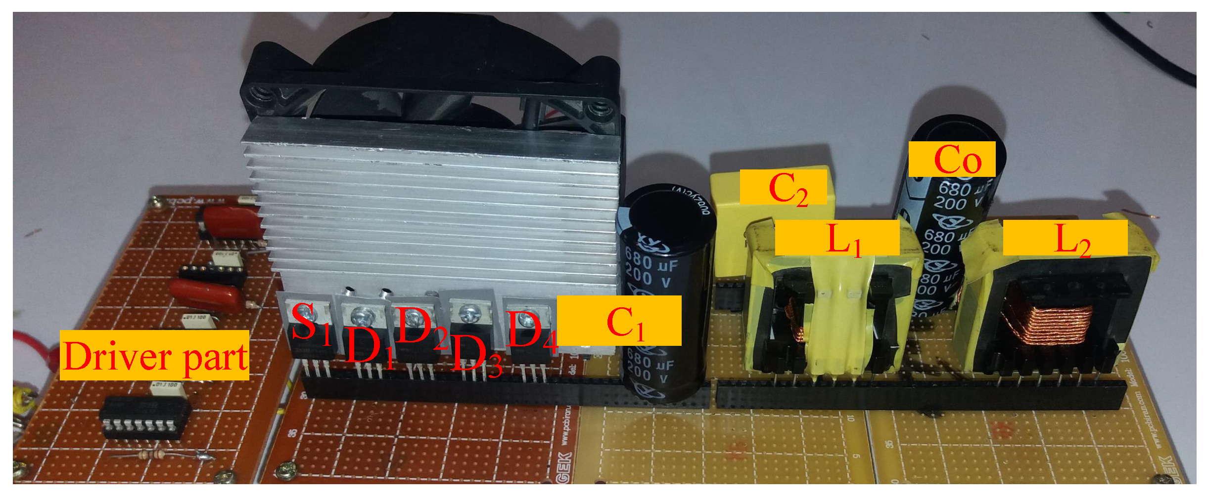
8. Simulation and the Experimental Results

To verify the validity of the extracted theoretical relations, the simulation and the experimental results were extracted and compared with each other. The simulation software that was used to verify the correctness of the extracted relations was PLECS. The values of the inductors and capacitors were calculated by the written relations of the second section. The assumed values of the capacitors average voltage and the inductors average current were:
I L 1 = 6 A , I L 2 = 4 A , Δ i L I L = 30 p e r c e n t , f s = 100 kHz , P o = 120 W V C 1 = 40 V , V C 2 = 40 V , V C o = 120 V , Δ v C V C = 5 p e r c e n t
Consequently, the inductor and the capacitor values are written as:
L 1 = 55 μ H , L 2 = 333 μ H , C 1 = 10 μ F , C 2 = 5 μ F , C o = 1.66 μ F
The simulation results of the converter are illustrated in Figure 10. Based on the extracted values, the average value of the capacitor voltage and the inductors current are calculated as:
I L 1 = 6 A , I L 2 = 2 A , V C 1 = 40 V , V C 2 = 40 V , V C o = 118 V
A comparison between the extracted values and the assumed values defines the compatibility of the values. The experimental results are shown in Figure 11 and Figure 12. Similar to the simulation results, the wave form of the voltage of the capacitors, the current of the inductors, and the current of semiconductors circuit components were extracted. The frequency was set to 100 kHz, and IRF2110 was used as the MOSFET drives of the circuits. The switch and diode type were IRF540 and 2015OCT, respectively. The extracted values of the capacitor voltage and the inductor current are written as:
I L 1 = 6 A , I L 2 = 2 A , V i n = 20 V , V C 1 = 40 V , V C 2 = 40 V , V C o = 120 V
A comparison among the experimental simulation results and the assumed values, defines the compatibility of the values. The built-up converter is illustrated in Figure 13. In Figure 14, the non-ideal voltage gain of the proposed converter based on its extracted relations si compared with the practical voltage gain of the proposed converter when the duty cycle varies from 20 percent to 80 percent. The non-ideal voltage gain relation is expressed as the non-ideal behaviour of the proposed converter in a suitable way.
In Figure 15, the efficiency of the proposed converter was extracted for the different values of the output power. This was set for the 50 percent duty cycle and the output voltage of 120 V. From Figure 15, the output power varied from 30 to 210 W. The efficiency of the proposed converter was more than 90 percent. Therefore, the high value of the voltage gain was achieved by a high value of the efficiency, which makes it suitable for renewable applications.
From Figure 15, the efficiency of the designed converter based on the extracted relations was 92.6 percent with the output power of 120 W and output voltage of 120 V. The mentioned value based on the experimental results was extracted at 91 percent, and its pie chart is illustrated in Figure 16a. According to Figure 16b, the diode loss, the switch loss, and inductor loss were the highest losses of the mentioned converter.

9. Conclusions

We evolved a step-up DC-DC converter from cascaded boost and Lou converters. This converter benefits from various advantages, such as a high voltage gain ratio without any transformer deployment, good efficiency, continuity of the input current, and the utilization of only one power switch. Various comparisons were undertaken in terms of the voltage gain, efficiency, and component stress in order to demonstrate the supremacy of the proposed converter in comparison with the existing quadratic DC-DC converters and its suitability for renewable energy applications.
Small signal analysis of the proposed topology was performed, and its bode diagram was extracted for both before and after compensation. A suitable compensator was designed using the sisotool tool box of MATLAB. The compatibility of the simulation and experimental results with the theoretical calculations validated the study and confirmed that the proposed converter can be employed in suitable renewable applications.

Author Contributions

Conceptualization, H.G., E.A. and S.A.G.; methodology, M.R.H. and R.S.S.; software, H.G.; validation, R.S.S., M.R.H. and H.G.; formal analysis, H.G.; investigation, H.G.; resources, H.G.; writing—original draft preparation, H.G., R.S.S. and M.R.H.; writing—review and editing, H.G., E.A., S.A.G.; supervision, E.A., S.A.G.; project administration, H.G.; All authors have read and agreed to the published version of the manuscript.

Funding

This research received no external funding.

Conflicts of Interest

The authors declare no conflict of interest.

Appendix A

Table A1. Comparison of the voltage/current stresses.
V S 1 V O V S 2 V O V D 1 V O V D 2 V O I S 1 I in I S 2 I in I D 1 I in I D 2 I in D
[10] 1 D D 2 = 0.571 1 D D 2 = 0.57 1 D = 1.41 1 D D = 0.41 1 D D = 0.41 1 D D 2 = 0.170.71
[11] 1 D D 2 = 0.57 1 D = 1.4 1 D D 2 = 0.57 1 D = 1.41 1 D D = 0.41 1 D D = 0.41 1 D D 2 = 0.170.71
[12] 1 D 2 = 1.96 1 D = 1.4 1 D D 2 = 0.57 1 D = 1.41 2 D 1 D = 0.6 2 D 1 D = 0.6 1 D D 2 = 0.170.71
[13] 1 D D 2 = 0.57 1 D = 1.4 1 D D 2 = 0.57 1 D = 1.41 1 D D = 0.41 1 D D = 0.41 1 D D 2 = 0.170.71
[14] 1 D D 2 = 0.57 1 D = 1.4 1 D D 2 = 0.57 1 D = 1.41 1 D D = 0.41 1 D D = 0.41 1 D D 2 = 0.170.71
[15] 1 D D 2 = 0.57 1 D = 1.4 1 D D 2 = 0.57 1 D = 1.41 1 D D = 0.41 1 D D = 0.41 1 D D 2 = 0.170.71
[16] 1 D D 2 = 0.57 1 D = 1.4 1 D D 2 = 0.57 1 D = 1.41 1 D D = 0.41 1 D D = 0.41 1 D D 2 = 0.170.71
[17] 1 D D 2 = 0.73 2 D 1 D = 0.51 1 D D = 0.4912 − D = 1.331 − D = 0.33 1 D D = 0.49 ( 1 D ) 2 D = 0.160.67
[18] 1 D D = 0.49 1 D = 1.5 1 D D = 0.49 1 D = 1.5D = 0.671 − D = 0.331 − D = 0.33 ( 1 D ) 2 D = 0.160.67
[19] 1 D D = 0.491 1 D D = 0.49111 − D = 0.33 1 D D = 0.49 ( 1 D ) 2 D = 0.160.67
[20] 1 D D = 0.49 1 D = 1.5 1 D D = 0.49 1 D = 1.5D = 0.671 − D = 0.331 − D = 0.33 ( 1 D ) 2 D = 0.160.67
[21] 1 D D ( 2 D ) = 0.72 1 D ( 2 D ) = 1.84 1 D D ( 2 D ) = 0.72 1 D ( 2 D ) = 1.84 1 D ( 2 D ) = 1.84 1 D 2 D = 0.28 1 D D ( 2 D ) = 0.72 ( 1 D ) 2 D ( 2 D ) = 0.280.61
[22] 1 D D ( 2 D ) = 0.72 1 D ( 2 D ) = 1.84 1 D D ( 2 D ) = 0.72 1 D = 1.64 1 2 D = 0.72 1 D 2 D = 0.28 1 D 2 D = 0.28 ( 1 D ) 2 D ( 2 D ) = 0.280.61
[9]1 − D = 0.411 − D = 0.42 − D = 1.4D = 0.6D(1 − D) = 0.24D(1 − D) = 0.24(1 − D) 2 = 0.160.6
Table A2. Comparison of the power loss.
Inductors LossSwitches Conduction LossSwitching Loss of SwitchesDiodes LossDuty Cycle
proposed converters P o r L R 2 D 2 6 D + 5 ( 1 D ) 4 , 40 P o r L R P o r S R ( D 2 + D + 1 ) 2 D ( 1 D ) 4 , 50 P o r S R f s P o t o f f ( 1 + D D 2 ) 2 ( 1 D ) 2 ( 2 D ) , 6.67 f s P o t o f f V D F I o ( 2 D 2 5 D + 4 ) ( 1 D ) 2 , 8 V D F I o 0.5
[10] P o r L R D 4 2 D 3 + 3 D 2 2 D + 1 ( 1 D ) 4 , 77 P o r L R P o r S R 2 D 3 2 D 2 + D ( 1 D ) 4 , 50.12 P o r S R f s P o t o f f ( 1 + D ) 1 D , 5.66 f s P o t o f f V D F I o 1 D , 3.93 V D F I o 0.7
[11] P o r L R 2 D 4 6 D 3 + 8 D 2 4 D + 1 ( 1 D ) 4 , 66.93 P o r L R P o r S R 2 D 3 2 D 2 + D ( 1 D ) 4 , 50.12 P o r S R f s P o t o f f 1 D , 3.33 f s P o t o f f V D F I o 1 D , 3.33 V D F I o 0.7
[12] P o r L R 3 D 4 5 D 3 + 7 D 2 4 D + 1 ( 1 D ) 4 , 78.43 P o r L R P o r S R 5 D 3 4 D 2 + D ( 1 D ) 4 , 56.17 P o r S R f s P o t o f f D ( 1 D ) 2 , 7.77 f s P o t o f f V D F I o 1 D , 3.33 V D F I o 0.7
[13] P o r L R 2 D 4 6 D 3 + 8 D 2 4 D + 1 ( 1 D ) 4 , 66.93 P o r L R P o r S R 2 D 3 2 D 2 + D ( 1 D ) 4 , 50.12 P o r S R f s P o t o f f 1 D , 3.33 f s P o t o f f V D F I o 1 D , 3.33 V D F I o 0.7
[14] P o r L R 2 D 2 2 D + 1 ( 1 D ) 4 , 71.6 P o r L R P o r S R 2 D 3 2 D 2 + D ( 1 D ) 4 , 50.12 P o r S R f s P o t o f f 1 D , 3.33 f s P o t o f f V D F I o 1 D , 3.33 V D F I o 0.7
[15] P o r L R 2 D 2 2 D + 1 ( 1 D ) 4 , 71.6 P o r L R P o r S R 2 D 3 2 D 2 + D ( 1 D ) 4 , 50.12 P o r S R f s P o t o f f 1 D , 3.33 f s P o t o f f V D F I o 1 D , 3.33 V D F I o 0.7
[16] P o r L R 5 D 2 6 D + 2 ( 1 D ) 4 = 30.86 P o r L R P o r S R 5 D 3 6 D 2 + 2 D ( 1 D ) 4 , 21.6 P o r S R f s P o t o f f ( 3 D 1 ) D ( 1 D ) , 5.23 f s P o t o f f V D F I o 1 D , 3.33 V D F I o 0.7
[17] P o r L R 3 D 2 4 D + 2 ( 1 D ) 4 , 18.7 P o r L R P o r S R 2 D 3 6 D 2 + 5 D ( 1 D ) 4 , 106.1 P o r S R f s P o t o f f ( 1 + D ) 1 D , 5.1 f s P o t o f f V D F I o ( 1 + D ) 1 D , 5.1 V D F I o 0.67
[18] P o r L R 2 D 4 6 D 3 + 8 D 2 4 D + 1 ( 1 D ) 4 , 42.97 P o r L R P o r S R 2 D 3 2 D 2 + D ( 1 D ) 4 , 31.51 P o r S R f s P o t o f f ( 1 + D ) 1 D , 5.1 f s P o t o f f V D F I o 1 D , 3 V D F I o 0.67
[19] P o r L R D 2 2 D + 2 ( 1 D ) 4 , 93.5 P o r L R P o r S R D 3 2 D 2 + 2 D ( 1 D ) 4 , 62.64 P o r S R f s P o t o f f ( 1 + D ) 1 D , 5.1 f s P o t o f f V D F I o ( 2 D ) 1 D , 4 V D F I o 0.67
[20] P o r L R 2 D 2 2 D + 1 ( 1 D ) 4 , 131.35 P o r L R P o r S R 2 D 3 2 D 2 + 2 D ( 1 D ) 4 , 31.51 P o r S R f s P o t o f f ( 1 + D ) 1 D , 5.1 f s P o t o f f V D F I o 1 D , 3 V D F I o 0.67
[21] P o r L R 2 D 2 2 D + 1 ( 1 D ) 4 , 14.91 P o r L R P o r S R D 3 2 D 2 + D ( 1 D ) 4 , 19.75 P o r S R f s P o t o f f ( 1 D ) ( 2 D ) , 1.62 f s P o t o f f V D F I o ( 1 + D ) 1 D , 3.65 V D F I o 0.57
[22] P o r L R D 4 4 D 3 + 8 D 2 4 D + 1 ( 1 D ) 4 , 20 P o r L R P o r S R D 3 2 D 2 + 2 D ( 1 D ) 4 , 19.75 P o r S R f s P o t o f f ( 1 D ) ( 2 D ) , 1.62 f s P o t o f f V D F I o 1 D , 2.32 V D F I o 0.57
[9] P o r L R D 2 2 D + 2 ( 1 D ) 4 , 31.84 P o r L R P o r S R D 3 2 D 2 + D ( 1 D ) 4 , 2.9 P o r S R f s P o t o f f ( 3 D D 2 ) ( 1 D ) , 3.1 f s P o t o f f V D F I o 1 D , 2.37 V D F I o 0.56

References

  1. Li, W.; Lv, X.; Deng, Y.; Liu, J.; He, X. A Review of Non-Isolated High Step-Up DC/DC Converters in Renewable Energy Applications. In Proceedings of the 2009 Twenty-Fourth Annual IEEE Applied Power Electronics Conference and Exposition, Washington, DC, USA, 21 March 2009; pp. 364–369. [Google Scholar]
  2. Marjani, J.; Imani, A.; Hekmati, A.; Afjei, E. A new dual output DC-DC converter based on SEPIC and Cuk converters. In Proceedings of the 2016 International Symposium on Power Electronics, Electrical Drives, Automation and Motion (SPEEDAM), Capri, Italy, 1 August 2016; pp. 946–950. [Google Scholar]
  3. Gopi, R.R.; Sreejith, S. Converter topologies in photovoltaic applications—A review. Renew. Sustain. Energy Rev. 2018, 94, 1–14. [Google Scholar] [CrossRef]
  4. Amir, A.; Amir, A.; Che, H.S.; Elkhateb, A.; Abd Rahim, N. Comparative analysis of high voltage gain DC-DC converter topologies for photovoltaic systems. Renew. Energy 2019, 136, 1147–1163. [Google Scholar] [CrossRef] [Green Version]
  5. Tewari, N.; Sreedevi, V. A novel single switch DC-DC converter with high voltage gain capability for solar PV based power generation systems. Sol. Energy 2018, 171, 466–477. [Google Scholar] [CrossRef]
  6. Revathi, B.S.; Prabhakar, M. Non isolated high gain DC-DC converter topologies for PV applications—A comprehensive review. Renew. Sustain. Energy Rev. 2016, 66, 920–933. [Google Scholar] [CrossRef]
  7. Taghvaee, M.; Radzi, M.; Moosavain, S.; Hizam, H.; Marhaban, M.H. A current and future study on non-isolated DC–DC converters for photovoltaic applications. Renew. Sustain. Energy Rev. 2013, 17, 216–227. [Google Scholar] [CrossRef]
  8. Forouzesh, M.; Siwakoti, Y.P.; Gorji, S.A.; Blaabjerg, F.; Lehman, B. Step-Up DC–DC Converters: A Comprehensive Review of Voltage-Boosting Techniques, Topologies, and Applications. IEEE Trans. Power Electron. 2017, 32, 9143–9178. [Google Scholar] [CrossRef]
  9. Golizedeh, H.; Hashemi, M.R.; Rafiee, Z.; Hamzeh, M.; Afjei, E. A Quadratic Boost Converter with Continuous Input Current and Suitable for Photo Voltaic Solar Panels. In Proceedings of the 2020 28th Iranian Conference on Electrical Engineering (ICEE), Tabriz, Iran, 26 November 2020; pp. 1–5. [Google Scholar]
  10. Gholizadeh, H.; Salehi, M.; Rafiee, Z.; Afjei, E.; Hamzeh, M. A Transformer less Quadratic Buck-Boost Converter with Wide Range of Output Voltage and Low Switch Stresses. In Proceedings of the 2020 11th Power Electronics, Drive Systems, and Technologies Conference (PEDSTC), Tehran, Iran, 4–6 February 2020; pp. 1–6. [Google Scholar]
  11. Miao, S.; Wang, F.; Ma, X. A New Transformerless Buck-Boost Converter With Positive Output Voltage. IEEE Trans. Ind. Electron. 2016, 63, 2965–2975. [Google Scholar] [CrossRef]
  12. Sarikhani, A.; Allahverdinejad, B.; Hamzeh, M.; Afjei, E. A continuous input and output current quadratic buck-boost converter with positive output voltage for photovoltaic applications. Sol. Energy 2019, 188, 19–27. [Google Scholar] [CrossRef]
  13. Gholizadeh, H.; Sarikhani, A.; Hamzeh, M. A Transformerless Quadratic Buck-Boost Converter Suitable for Renewable Applications. In Proceedings of the 2019 10th International Power Electronics, Drive Systems and Technologies Conference (PEDSTC), Shiraz, Iran, 25 April 2019; pp. 470–474. [Google Scholar]
  14. Babazadeh, Y.; Babaei, E.; Sabahi, M. A New Non-Isolated Buck-Boost Converter with High Voltage Gain and Positive Output Voltage for Renewable Energy Applications. In Proceedings of the 2019 10th International Power Electronics, Drive Systems and Technologies Conference (PEDSTC), Shiraz, Iran, 25 April 2019; pp. 201–206. [Google Scholar]
  15. Rosas-Caro, J.C.; Valdez-Resendiz, J.E.; Mayo-Maldonado, J.C.; Alejo-Reyes, A.; Valderrabano-Gonzalez, A. Quadratic buck–boost converter with positive output voltage and minimum ripple point design. IET Power Electron. 2018, 11, 1306–1313. [Google Scholar] [CrossRef]
  16. Rosas-Caro, J.C.; Sanchez, V.M.; Valdez-Resendiz, J.E.; Mayo-Maldonado, J.C.; Beltran-Carbajal, F.; Valderrabano-Gonzalez, A. Quadratic buck-boost converter with positive output-voltage and continuous input-current. In Proceedings of the 2018 International Conference on Electronics, Communications and Computers (CONIELECOMP), Cholula, Mexico, 21–23 February 2018; pp. 152–158. [Google Scholar]
  17. Totonchi, N.; Gholizadeh, H.; Afjei, E.; Hamzeh, M. A Novel Transformer less High Gain DC-DC Converter with Continuous Input Current and Suitable for Photo Voltaic Panels. In Proceedings of the 2020 11th Power Electronics, Drive Systems, and Technologies Conference (PEDSTC), Tehran, Iran, 4–6 February 2020; pp. 1–6. [Google Scholar]
  18. Gholizadeh, H.; Aboufazeli, S.; Rafiee, Z.; Afjei, E.; Hamzeh, M. A Non-Isolated High Gain DC-DC Converters with Positive Output Voltage and Reduced Current Stresses. In Proceedings of the 2020 11th Power Electronics, Drive Systems, and Technologies Conference (PEDSTC), Tehran, Iran, 4–6 February 2020; pp. 1–6. [Google Scholar]
  19. Garcia-Vite, P.M.; Soriano-Rangel, C.A.; Rosas-Caro, J.C.; Mancilla-David, F. A DC-DC converter with quadratic gain and input current ripple cancelation at a selectable duty cycle. Renew. Energy 2017, 101, 431–436. [Google Scholar] [CrossRef]
  20. Garcia-Vite, P.M.; Valdez-Resendiz, J.E.; Mayo-Maldonado, J.C.; Rosas-Caro, J.C.; Rosario Rivera-Espinosa, M.; Valderrabano-Gonzalez, A. Quadratic gain converter with output voltage ripple mitigation. In Proceedings of the 2017 IEEE Energy Conversion Congress and Exposition (ECCE), Cincinnati, OH, USA, 1–5 October 2017; pp. 2253–2259. [Google Scholar]
  21. Ding, S.; Wang, F. A New Negative Output Buck–Boost Converter with Wide Conversion Ratio. IEEE Trans. Ind. Electron. 2017, 64, 9322–9333. [Google Scholar] [CrossRef]
  22. Gholizadeh, H.; Babazadeh-Dizaji, R.; Hamzeh, M. High-Gain Buck-Boost Converter Suitable for Renewable Applications. In Proceedings of the 2019 27th Iranian Conference on Electrical Engineering (ICEE), Yazd, Iran, 30 April–2 May 2019; pp. 777–781. [Google Scholar]
Figure 1. (a) A boosting circuit, and (b) a Luo converter.
Energies 14 03584 g001
Figure 2. (a) The proposed topology, (b) how it was made, (c) the equivalent circuit of the first mode, and (d) the equivalent circuit of the second mode.
Energies 14 03584 g002
Figure 3. The comparison of the ideal voltage gain of the proposed converter with the conventional converters and various types of the quadratic converters.
Energies 14 03584 g003
Figure 4. The comparison of the ideal and non-ideal voltage gain of the proposed converter.
Energies 14 03584 g004
Figure 5. The comparison of the non-ideal voltage gain of the proposed converter with the quadratic boost and Luo converters.
Energies 14 03584 g005
Figure 6. The comparison of the non-ideal voltage gain of the proposed converter with the mentioned converters of [9,10,11,12,13,14,15,16,17,18,19,20,21,22].
Energies 14 03584 g006
Figure 7. The comparison of the efficiency of the proposed converter with the boosting circuit and Luo converter.
Energies 14 03584 g007
Figure 8. The efficiency of the proposed converter for the various values of the output power, (a) while the duty cycle varied from 0 to 50 percent, and (b) while the duty cycle varied from 50 to 100 percent.
Energies 14 03584 g008
Figure 9. The bode diagram (a) before compensating, and (b) after compensating.
Energies 14 03584 g009
Figure 10. Simulation results: the (a) current of L 1 , (b) current of L 2 , (c) voltage of C 1 , (d) voltage of C 2 , (e) voltage of C o , (f) current of S 1 , (g) current of D 1 , (h) current of D 2 , (i) current of D 3 , and (j) current of D 4 .
Energies 14 03584 g010
Figure 11. The extracted voltage wave forms of the capacitors and the current wave forms of the inductors from the experimental results.
Energies 14 03584 g011
Figure 12. The extracted current waveform of the semiconductor devices.
Energies 14 03584 g012
Figure 13. The prototype.
Energies 14 03584 g013
Figure 14. The comparison of the non-ideal voltage gain based on the extracted relations and practical voltage gain based on the experimental results.
Energies 14 03584 g014
Figure 15. The efficiency of the proposed converter for the various value of the output power and 50 percent of the duty cycle.
Energies 14 03584 g015
Figure 16. The output power was set at 120 W: (a) pie chart of the efficiency and power losses, and (b) the percentage of the power losses.
Energies 14 03584 g016
Table 1. Comparison of the voltage/current stresses.
V S 1 V O V S 2 V O V D 1 V O V D 2 V O I S 1 I in I S 2 I in I D 1 I in I D 2 I in D
[10]0.5710.571.410.410.410.170.71
[11]0.571.40.571.410.410.410.170.71
[12]1.961.40.571.410.60.60.170.71
[13]0.571.40.571.410.410.410.170.71
[14]0.571.40.571.410.410.410.170.71
[15]0.571.40.571.410.410.410.170.71
[16]0.571.40.571.410.410.410.170.71
[17]0.730.510.4911.330.330.490.160.67
[18]0.491.50.491.50.670.330.330.160.67
[19]0.4910.49110.330.490.160.67
[20]0.491.50.491.50.670.330.330.160.67
[21]0.721.840.721.841.840.280.720.280.61
[22]0.721.840.721.640.720.280.280.280.61
[9]0.410.41.40.60.240.240.160.6
Table 2. Comparison of power loss.
Inductors LossSwitches Conduction LossSwitching Loss of SwitchesDiodes LossDuty Cycle
proposed 40 P o r L R 50 P o r S R 6.67 f s P o t o f f 8 V D F I o 0.5
[10] 77 P o r L R 50.12 P o r S R 5.66 f s P o t o f f 3.93 V D F I o 0.7
[11] 66.93 P o r L R 50.12 P o r S R 3.33 f s P o t o f f 3.33 V D F I o 0.7
[12] 78.43 P o r L R 56.17 P o r S R 7.77 f s P o t o f f 3.33 V D F I o 0.7
[13] 66.93 P o r L R 50.12 P o r S R 3.33 f s P o t o f f 3.33 V D F I o 0.7
[14] 71.6 P o r L R 50.12 P o r S R 3.33 f s P o t o f f 3.33 V D F I o 0.7
[15] 71.6 P o r L R 50.12 P o r S R 3.33 f s P o t o f f 3.33 V D F I o 0.7
[16] 30.86 P o r L R 21.6 P o r S R 5.23 f s P o t o f f 3.33 V D F I o 0.7
[17] 18.7 P o r L R 106.1 P o r S R 5.1 f s P o t o f f 5.1 V D F I o 0.67
[18] 42.97 P o r L R 31.51 P o r S R 5.1 f s P o t o f f 3 V D F I o 0.67
[19] 93.5 P o r L R 62.64 P o r S R 5.1 f s P o t o f f 4 V D F I o 0.67
[20] 131.35 P o r L R 31.51 P o r S R 5.1 f s P o t o f f 3 V D F I o 0.67
[21] 14.91 P o r L R 19.75 P o r S R 1.62 f s P o t o f f 3.65 V D F I o 0.57
[22] 20 P o r L R 19.75 P o r S R 1.62 f s P o t o f f 2.32 V D F I o 0.57
[9] 31.84 P o r L R 2.9 P o r S R 3.1 f s P o t o f f 2.37 V D F I o 0.56
Publisher’s Note: MDPI stays neutral with regard to jurisdictional claims in published maps and institutional affiliations.

