Article

Characterization of Potential-Induced Degradation and Recovery in CIGS Solar Cells

1
Department of Materials Science and Engineering, Korea University, Seoul 02841, Korea
2
National Agenda Research Division, Korea Institute of Science and Technology (KIST), Seoul 02792, Korea
3
Photovoltaics Laboratory, Korea Institute of Energy Research, Daejeon 34129, Korea
4
Graduate School of Energy and Environment (KU-KIST Green School), Korea University, Seoul 02841, Korea
*
Authors to whom correspondence should be addressed.
Equal contribution authorship.
Energies 2021, 14(15), 4628; https://doi.org/10.3390/en14154628
Submission received: 22 June 2021 / Revised: 20 July 2021 / Accepted: 23 July 2021 / Published: 30 July 2021
(This article belongs to the Special Issue Inorganic Nanocrystal Solar Cells)

Abstract

:
The potential-induced degradation (PID) mechanism in Cu(In,Ga)(Se,S)2 (CIGS) thin-film solar cells, which are alternative energy sources with a high efficiency (>23%) and upscaling possibilities, remains unclear. Therefore, the cause of PID in CIGS solar cells was investigated in this study at the cell level. First, an appropriate PID experiment structure at the cell level was determined. Subsequently, PID and recovery tests were conducted to confirm the PID phenomenon. Light current–voltage (I–V), dark I–V, and external quantum efficiency (EQE) analyses were conducted to determine changes in the cell characteristics. In addition, capacitance–voltage (C–V) measurements were carried out to determine the doping concentration and width of the space charge region (SCR). Based on the results, the causes of PID and recovery of CIGS solar cells were explored, and it was found that PID occurs due to changes in the bulk doping concentration and built-in potential at the junction. Furthermore, by distinguishing the effects of temperature and voltage, it was found that PID phenomena occurred when potential difference was involved.

1. Introduction

Based on global photovoltaic (PV) market statistics, the global cumulative PV capacity was 591 GW in 2019 [1]. The annual module production was 184 GW with Cu(In,Ga)(Se,S)2 (CIGS) commercial production of 1 GW at the end of 2019 [1]. CIGS solar cells have received increased attention. An economically feasible energy generation source must have a high energy conversion efficiency, low module degradation rate, and long life. Therefore, to ensure the long-term reliability of a PV module for a stable power supply, it is essential to understand and prevent degradation. Many studies have been conducted on module degradation based on various types of external environments [2]. Potential-induced degradation (PID) is a degradation phenomenon that has led to problems in the last few years [3,4,5]. It has been reported that PV module power degrades within a short amount of time owing to PID. Based on the literature, PID is generated as follows: when PV modules are connected in series, the module frames are grounded for safety and support reasons because a voltage > 600 V is generated. This leads to a relative potential difference between the grounded electrodes and solar cells inside the modules, which increases toward the end of the serial connection. Leakage current flows in solar cells due to the negative potential difference compared with the frame, and the power of the modules eventually decreases. This phenomenon is called PID.
The PID mechanism has been identified in both p- and n-type crystalline silicon solar cells, which are first-generation solar cells [6,7,8,9,10,11]. When a voltage is applied to p-type silicon solar cells, Na ions permeate into the stacking faults and act as shunt paths, resulting in degradation [6,7,8,9]. On the other hand, the accumulation of positive charges on the surface causes the electrons near the emitter to recombine, resulting in degradation in n-type solar cells [10,11]. It has been suggested that the migration of charges originating from glass mediates the leakage current in both cases. CIGS thin-film solar cells have a p-type absorption layer, and Na content of CIGS affects the property of the solar cells, where a certain amount of Na injection is used to improve the efficiency during solar cell fabrication [12,13,14,15]. The effects of externally introduced Na on PID are still unclear, however, it is expected that Na affects the PID mechanism of CIGS solar cells, similar to the case of silicon solar cells. Based on previous research on the PID mechanism, the degradation is greater in the case of samples with high Na concentration and low resistivity [16]. In previous studies, the width of the space charge region (SCR) was examined through capacitance–voltage (C–V) measurements. The results showed that the p–n junction in a sample with high Na concentration severely deteriorates due to PID [17]. Research has been carried out to clarify the PID mechanism of CIGS solar cells. The results of dark current–voltage (I–V) measurements before and after PID showed that the diode saturation current of soda–lime glass (SLG) samples increases and the shunt resistance decreases compared with those in the case of borosilicate glass (BSG) samples. This can be explained with the Na effect [18]. In addition, the results of secondary ion mass spectrometry (SIMS) and C–V measurements showed that cations accumulate at the junction, thereby decreasing the charge carrier concentration and changing the open-circuit voltage (VOC) and efficiency [19]. Based on time-of-flight secondary-ion mass spectrometry (TOF-SIMS) imaging and three-dimensional (3D) tomography, it was revealed that Na segregates into grain boundaries after PID [20]. However, in contrast with silicon solar cells, the cause of PID in CIGS solar cells and the corresponding recovery mechanism remain unclear.
In this study, the PID phenomenon was induced in a CIGS module at the cell level to identify the PID mechanism. Before proceeding with the PID test and recovery, PID test structures were designed at the cell level. In the case of silicon solar cells, a voltage is applied while the front and rear electrodes of the solar cell are short-circuited, according to IEC 62,804 [21]. Because PID occurs through the insulating thin film in most silicon solar cells, the structures in which the front and back electrodes are separately connected and those in which they are short-circuited exhibit the same effects. Therefore, it is assumed that the configurations of the solar cell electrodes are insignificant. On the other hand, in the case of thin-film solar cells, TCO layers exist on the outermost layer such that the electric fields inside the solar cells vary depending on the electrode configuration. In the past, voltage application experiments were conducted on multiple CIGS solar module and cell structures. These structures are shown in Figure 1. With respect to PID tests on CIGS solar modules, the voltage can be applied in three ways, that is, by connecting the junction box (JB) with the: (1) back glass, (2) frame, or (3) cover glass [22,23,24,25,26,27]. In addition, after forming a metal grid on the front surface of a single cell, the top glass is covered to create a module structure; subsequently, the bottom glass is connected to the back electrode (1) or front electrode (2) and voltage is applied [18,20,28]. In contrast with module structure-based test results, relatively few results have been reported regarding cell-level PID tests, where the effect of the cover glass on the front side of module could be ignored. Two methods can be used to apply voltage, that is, connecting the bottom glass with the back electrode or connecting the back electrode with the front TCO, with the bottom glass connected to the ground [17,29]. Therefore, test configurations were compared first before long time PID test. With the voltage application structure confirmed in the above experiment, PID and recovery experiments were conducted. The PID and recovery tendency were analyzed using light I–V, dark I–V, external quantum efficiency (EQE), and C–V measurements. Changes in the characteristics of the CIGS solar cells due to PID can be explained via degradation due to the voltage based on a comparison with the characteristics of another sample to which only temperature is applied.

2. Materials and Methods

2.1. Fabrication of CIGS Solar Cells

The CIGS solar cells were fabricated by using a standard method: 800 nm of Mo was deposited by direct current (DC) sputtering on soda-lime glass (SLG) substrates, followed by three-stage co-evaporation of CIGS, chemical bath deposition of 60 nm CdS, and radio frequency (RF) sputtering of 50 nm intrinsic ZnO and 250 nm indium tin oxide (ITO). Finally, Al metal was deposited on ITO layer.

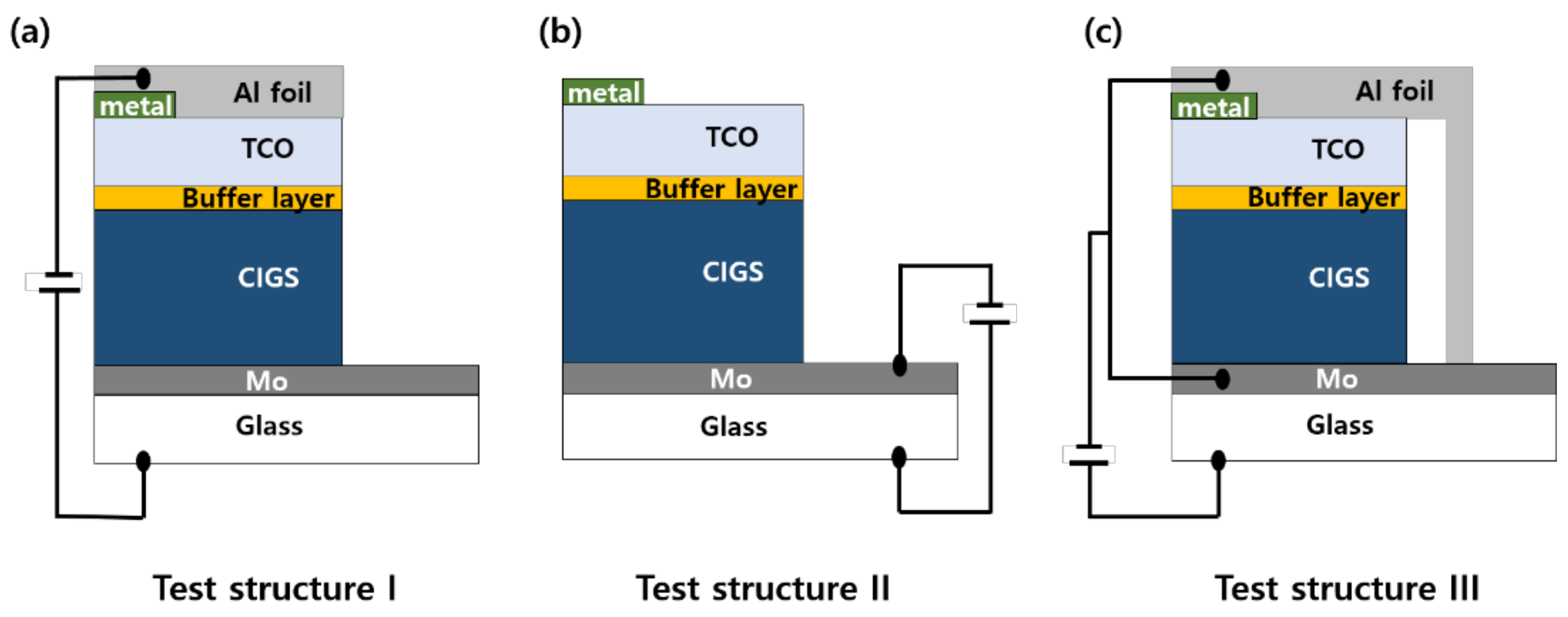
2.2. Design of the Voltage Application Structure for Potential-Induced Degradation

Three voltage application structures (Figure 2) were designed for the PID experiments on CIGS solar cells at the cell level. Figure 2a shows the structure to which a voltage is applied by connecting the anode to the glass side (rear) of the cell and the cathode to the transparent conducting oxide (TCO) side (front). Figure 2b shows a structure adopted from the literature [17]; an anode is connected to the glass side (rear), a cathode is connected to Mo (back electrode), and a voltage is applied. Further, a voltage is applied to the final structure shown in Figure 1c by connecting an anode to the glass side (rear) and a cathode to TCO, which was shorted with Mo. The second and third structures are similar in that there is no potential difference (same potential) from Mo to TCO. For voltage application, the samples are placed in a dark chamber to avoid light exposure and a voltage of 600 V is applied for 3 h at room temperature (RT) about 25 °C. The short voltage applying time 3 h is chosen because it is sufficient to distinguish undesirable degradation.

2.3. Potential-Induced Degradation and Recovery

The PID and recovery experiments were performed using the experimental structure determined in above experiment. All experiments were conducted in atmosphere, and relative humidity was not controlled. During the PID test in the dark chamber, a voltage of 600 V was applied for 24 h and the temperature was increased to 85 °C to accelerate the degradation. When the voltage was applied, an Al foil was used to cover the front of the sample to facilitate contact. To confirm the effect of voltage, another sample was maintained at 85 °C with no applied bias. Recovery started immediately after sample degradation and continued for 12 days. Subsequently, the samples were stored in the chamber at RT. The samples were measured in the initial state and after degradation and recovery. Changes in the solar cell characteristics were determined using light I–V, dark I–V, and EQE measurements. In addition, C–V measurements were carried out to analyze the changes in the doping concentration and SCR width.

2.4. Characterization

Light I–V measurements were performed with a Xe lamp solar simulator (WXS-155S-10, Class-AAA, WACOM, Japan). Dark I–V measurements were carried out by creating a contact between the cell and a 4-point probe of a source meter (2651A, Keithley, USA) and applying voltage from 0 to 1 V. To evaluate the electrical property regarding recombination of the device, the EQE measurements were performed with a 150 W Xe lamp (QEX7, PV measurement, USA) and a monochromator to provide monochromatic light in the wavelength range from 300 to 1100 nm. The C–V measurements were performed at 200 kHz and a voltage range of −1 to 1 V (CompactStat.h, IVIUM, Netherlands). By using C-V results, charge densities is calculated from Mott−Schottky analysis. Dynamic SIMS measurements were performed at the Korea Institute of Science and Technology (KIST) (IMS 4FE7, Cameca, France).

3. Results

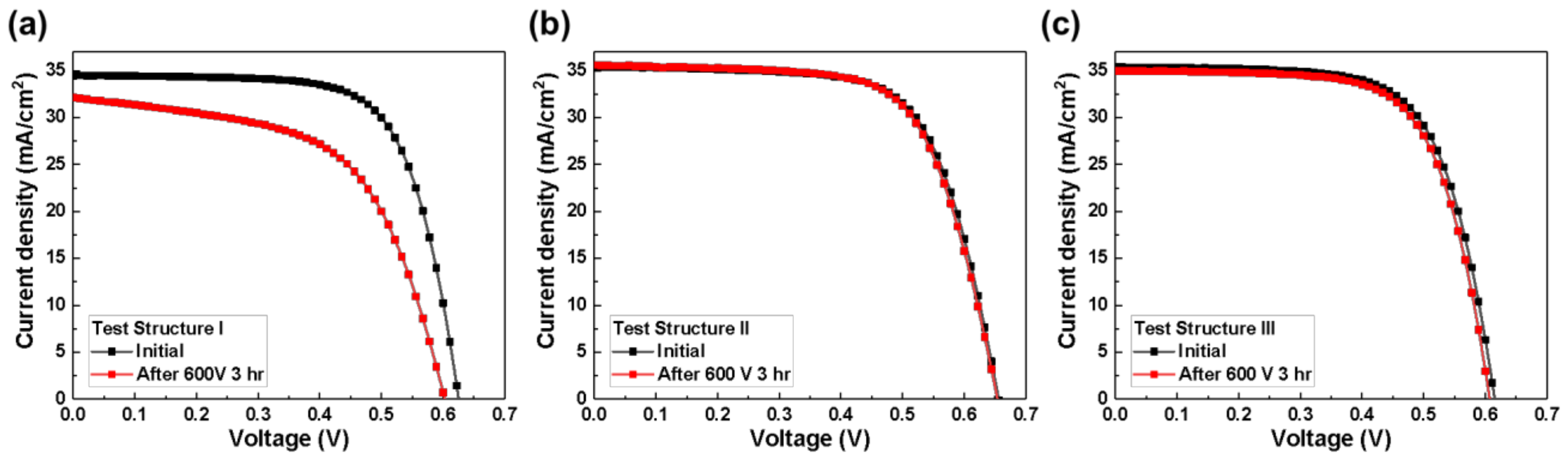
3.1. Design of the Voltage Application Structure for the PID Experiment by Short-Term Biasing Test

After applying a voltage to the CIGS solar cells and examining the changes of parameters, as shown in Figure 3 and Table 1, it can be seen that the efficiency (Eff) decreased significantly in a short time of 3 h when the voltage was applied like test structure I (Figure 2a). Based on prior reports, PID occurs within a relatively short amount of time (~10 h) at a temperature of 85 °C [16,18,30]. In addition, fill factor (FF) and VOC reductions due to the reduction of the shunt resistance were reported more frequently than decreases in the current density (JSC) [16,22,31,32]. However, in the case of test structure I in this study, not only the decrease in FF and VOC due to the decrease in shunt resistance, but also the decrease in the JSC due to the increase in series resistance occurred, the efficiency was greatly reduced by about 4% point. The efficiency of test structure I significantly decreases because an electric field forms inside the cell such that the current flows directly from the rear glass to the front TCO electrode. Therefore, test structure I is unsuitable for replicating the PID phenomenon. In contrast, the cell characteristics of test structures II and III (Figure 2b,c) insignificantly decrease when a voltage of 600 V is applied for 3 h. No current flows inside the cells, and the front and back electrodes of the cells in test structures II and III have the same potentials as the glass substrate. Therefore, potential differences are only induced in the glasses and Mo electrodes. The results show that the efficiency reductions in both the second and third structures are insignificant after 3 h of voltage application at RT. In the PID experiment, ions or elements inside the glass or CIGS solar cells drift or diffuse due to the application of temperature and voltage. In both structures II and III, the ions or elements move by diffusion due to the temperature gradient because there is no internal electromotive force for movement after ions from the glass are introduced and reach the Mo surface by applied voltage. Muzzillo reported that the degradation is accelerated if a solar cell is short-circuited or a forward bias is applied and that the degradation is benign if the solar cell has an open circuit [30]. However, the difference in the degree of degradation between the two structures was insignificant. When solar cells are actually driven, charges are continuously supplied by the photocurrent and an environment in which a neutral charge can be achieved is created when charges causing PID flow into CIGS from the outside. In the case of structure III, current flow cannot be observed; however, the structure entails a short circuit and the charge can be neutralized, similar to the case of the operation of solar cells. However, an open circuit cannot be neutralized until charge relaxation occurs completely, that is, until the charge relaxation time. Therefore, there is a possibility that other degradation factors play roles in test structure II compared with the actual PID case. Therefore, in this experiment, the PID test was performed by using test structure III. A long-term experiment was not carried out on test structure II to focus on the aims of this study.

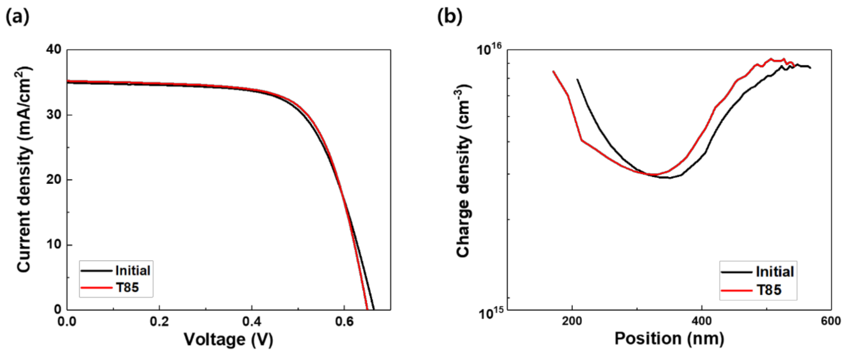
3.2. Potential-Induced Degradation and Recovery

After carrying out the PID test by applying 600 V at 85 °C for 24 h in a dark chamber, the cell was stored in the chamber at RT for 12 days for recovery. The CIGS solar cell characteristics were measured immediately after PID and recovery. The light J–V curve in Figure 4 confirms that the efficiency decreases from 15.43% to 9.26%, which is ~60% of the initial efficiency after deterioration, and then returns to 14.73% after the recovery. Although the initial JSC value is maintained, VOC and FF decrease to ~74% and 79% of the initial levels, respectively, after deterioration and then recover. The parameters are shown in Table 2. Subsequently, the sun-shaded method was used to compare the light J–V data at 1 sun and 0.2 sun to analyze the cause of the FF reduction [33]. Based on the parameter differences, the series resistance (Rs), shunt resistance (Rsh), n-factor, and empirical fill factor (FFideal, FFn, FFs, FFsh, FFcal) were calculated for the initial, PID, and recovery states [33,34]. The parameter FFideal represents the ideal FF; FFn is the FF considering the n-factor; and FFs, FFsh, and FFcal are the FFs considering the series and shunt resistances, respectively. Table 3 shows the comparison between the series resistance, shunt resistance, and n-factor results calculated by using the sun-shaded method and the results from light I–V measurements. Table 4 lists the calculated FFs. Based on the comparison of FFcal with the measured FF, the series resistance determines the FF of the solar cell at all stages. In addition, based on the comparison of all parameters, FFs, FFsh, and FFn decrease after PID and then increase during the recovery. These results confirm that the change due to series resistance is the largest, and the FFn and shunt resistance, representing recombination, decrease and increase at a similar rate. A decrease in the shunt resistance during PID of CIGS solar cells has been previously reported [16,17,18]; it was argued that this decrease is mainly due to the formation of a shunt path by Na inflow at the buffer and bulk interface [20]. Based on the results of this experiment, it is expected that the shunt resistance decreases and then recovers due to a similar cause. The reduction in the series resistance and recombination will be discussed in the next paragraph. In summary, based on the light J–V results, VOC and FF mainly affect the efficiency change due to the PID phenomenon in CIGS solar cells, which is similar to the results reported in the literature [16,17,29]. In addition, because the characteristics of the solar cell recover in the absence of additional external conditions, such as a reverse voltage or temperature, it is expected that the factors that generate the PID in the CIGS solar cells change. A reversible and nonpermanent PID has been reported for CIGS solar cells in the past [16,17,31].
Dark I–V measurements were used to investigate the cause of the efficiency reduction due to PID. The leakage currents derived by the double-diode model are listed in Table 5. The results show that J02, which represents the junction properties after PID, insignificantly changes. It slightly decreases, whereas the J01 value corresponding to the CIGS bulk region mainly increases. After the recovery, this parameter returns to a value similar to that in the initial state.
Subsequently, the EQE was measured to confirm the changes in the recombination characteristics inside the solar cell. Figure 5a shows that the EQE results do not indicate any changes before and after PID. In the literature, it was reported that the TCO region degrades due to the influx of Na during the PID test of the thin-film module, resulting in the degradation of the solar cell characteristics [35,36]. However, an EQE change was not observed in that experiment. Therefore, it can be expected an optical loss did not occur. In addition, it is assumed that voltage application does not lead to the degradation of the solar cell material. In fact, because an electric field was not applied to the solar cell due to the short circuit between both electrodes of the CIGS, material degradation is unlikely because the high voltage was mainly applied to the substrate glass, which is an insulator. In addition, it is assumed that the carrier transport in the buffer/CIGS and CIGS/Mo heterojunction regions did not change. Based on the similarity of the EQE curves in the long wavelength region, the diffusion length of the bulk did not change either. The diffusion length can be derived from the relationship between the inverse internal quantum efficiency (IQE) and absorption depth [37]. Although this experiment was based on the nondestructive analysis of the solar cell with an upper electrode, it was difficult to measure the surface reflectance. Because there are no changes in the appearance and shape of the EQE and we assume that there is no significant change in the reflectance, the diffusion length is not expected to significantly change. In addition, it can be confirmed that PID is not due to increased recombination at the CdS/CIGS interface, CIGS bulk, and CIGS/Mo interface because the EQE in all wavelength regions, including the long-wavelength region, does not change. This can also be confirmed by the magnitude of the bias-dependent local ideality factor derived from dark I–V measurements, as shown in Figure 5b. Local ideality factor, n = q k T d V d l n I is proportional to the inverse slope of the ln(I)-V curve. The minimum values of the ideality factors in the initial, PID, and recovery states are similar. This indicates that the types of deep trap defects, energy level, and recombination mechanism that cause Shockley–Read–Hall recombination in the charge-neutral region did not change. On the other hand, the maximum values of the ideality factors in the low-voltage region associated with junction recombination decrease after PID. Breitenstein proved that the maximum values of these ideality factors change according to the location of the shallow trap level [38]. Therefore, it is expected that the ideality maximum changes due to the change of the shallow trap related to the carrier concentration in this experiment. Therefore, based on the combination of the light I–V results, according to which VOC and FF mainly decrease after PID, dark I–V results, according to which J01 mainly increases, and the unchanged EQE, it can be expected that the PID is caused by changes in the bulk doping concentration and built-in potential change at the junction. Based on the ideal diode equation, J01 is in inverse proportion to the doping concentration when the diffusion length is constant; therefore, it can be inferred that the increase in J01 originates from the decrease in the doping concentration.
The C–V measurements were conducted to directly determine the change in the doping concentrations during the initial, PID, and recovery states. The charge density shown in Figure 6 was calculated under each condition based on the Mott–Schottky plot derived from the C–V measurement results. Figure 6 confirms that the doping concentration significantly decreases after PID, over the entire inner depth direction of the bulk, and increases again after the recovery. Additionally, it can be confirmed that the depletion width increases after PID and then returns to the original width. The charge density results show that the built-in potential decreases and the saturation current increases with decreasing doping concentration; consequently, the decrease in VOC can be interpreted [18]. In addition, it is expected that the bulk resistivity increases due to the decrease in the doping concentration and that the series resistance decreases accordingly. In CIGS solar cells, the role of alkali ions differs depending on whether they are interstitial or substitutional. Interstitial elements are known to act as donors [14]. In the case of PID, the possibility of the formation of a bond with CIGS by replacing a point defect is low because a very low temperature is applied compared with the temperature at which the phase change occurs. However, when elements are introduced from the outside, they enter the interstitial sites and can act as donors. When the number of donor defects increases, the doping concentration of the entire device decreases. Therefore, it is expected that the doping concentration decreases after PID. Although an analysis in this regard was not performed in this study, it is presumed that the interstitial elements introduced into the grain boundaries with low chemical potential escape and the original bulk properties are restored during the recovery after PID to achieve a thermodynamically stable state.
Based on various analysis methods, attempts have been made to analyze the cause of PID in CIGS solar cells. However, it is necessary to analyze whether the PID is induced by the applied voltage or temperature. Therefore, another CIGS solar cell sample was exposed to a temperature of 85 °C for 24 h in the dark chamber. For convenience, this experiment is designated as T85. The changes in the characteristics of the sample are shown in Figure 7. Figure 7a,b show the light I–V and carrier concentration graphs for the solar cells. When only temperature was applied to the sample, unlike in the case of PID, both the solar cell characteristics and doping concentration changed insignificantly. Therefore, it can be assumed that the PID phenomena of CIGS solar cells are caused by the potential difference rather than the temperature.
For confirmation, SIMS analyses were performed on the samples to which only temperature was applied and on those in which Mo was deposited on the SLG substrate and a voltage and temperature were applied together (Figure 8). In general, in the co-evaporation process of depositing the CIGS absorber layer, the temperature increases to 550 °C; it is known that alkali ions inside the glass flow into the CIGS during the phase formation [39,40,41]. To improve the efficiency, a post-deposition treatment (PDT) during which additional Na and K were injected was applied. This treatment is generally performed at a temperature of 300 °C or above. It can be assumed that the diffusion of alkali ions into CIGS is smooth at a high temperature of 300 °C or above [42,43,44,45]. On the other hand, in the case of the PID test, the test temperature was 85 °C. Therefore, a difference in the amounts of elements flowing from the glass to the CIGS bulk depending on whether or not an external voltage was applied is expected. The SIMS results confirm that both Na and K, which are known to have a major influence on the efficiency of the CIGS solar cell, account for the largest proportion of the CIGS bulk when voltage was applied together with the temperature. When only temperature is applied, the Na concentration partially increases compared with the reference, but the increase can be considered as insignificant because the intensity is plotted on a log scale. In other words, based on the SIMS results, the PID phenomenon occurs in CIGS solar cells when alkali ions inside the glass first move to the Mo/glass interface due to voltage and then diffuse into the CIGS bulk without a potential difference due to the temperature application.

4. Conclusions

To facilitate the commercialization of CIGS solar cells, degradation must be analyzed and prevented. The PID has been examined in the past and experiments replicating the PID at the cell level have been conducted to determine its causes. In this study, the PID mechanism was investigated by analyzing samples after PID and recovery. This is because PID can be prevented only by understanding the correct mechanism. The information in the literature is based on the change of Na. The aims of this study were to explain both the changes of Na and electrical properties. After PID and recovery experiments, light I–V, dark I–V, EQE, and C–V measurements were conducted. Based on the results, PID occurs due to changes in the bulk doping concentration and built-in potential at the junction.
In addition, a T85 test was carried out on a CIGS solar cell to distinguish the effects of the voltage and temperature. Not only CIGS solar cells but also Mo substrates, deposited Mo on SLG substrates, were tested with T85 and PID. Based on these experiments, it can be concluded that PID occurs in CIGS solar cells when alkali ions move from SLG to the Mo/SLG interface due to the potential difference and then diffuse into the CIGS absorption layer due to temperature application.

Author Contributions

S.L. and S.B. contributed equally to this work. Conceptualization, S.L. and S.B.; methodology, S.J.P.; validation, J.G., J.Y. and Y.-J.E.; formal analysis, S.L.; investigation, S.B.; resources, S.B.; data curation, S.L.; writing—original draft preparation, S.L.; writing—review and editing, S.B.; visualization, S.B.; supervision, Y.K.; project administration, D.K.; funding acquisition, H.-S.L. All authors have read and agreed to the published version of the manuscript.

Funding

This work was conducted under the framework of the Research and Development Program of the Korea Institute of Energy Research (KIER) (C0-2401-01). This work was supported by the National Research Foundation of Korea (NRF) grant funded by the Korea government (MSIT). (NRF-2020R1A2C1011815). This work was supported by “Human Resources Program in Energy Technology” of the Korea Institute of Energy Technology Evaluation and Planning (KETEP), granted financial resource from the Ministry of Trade, Industry & Energy, Republic of Korea. (No. 20204010600470). This work was also supported by the KU-KIST Graduate School Project.

Conflicts of Interest

The authors declare no conflict of interest.

References

  1. Wilson, G.; Al-Jassim, M.M.; Metzger, W.; Glunz, S.W.; Verlinden, P.; Gang, X.; Mansfield, L.; Stanbery, B.J.; Zhu, K.; Yan, Y. The 2020 photovoltaic technologies roadmap. J. Phys. D Appl. Phys. 2020, 53, 493001. [Google Scholar] [CrossRef]
  2. Köntges, M.; Kurtz, S.; Packard, C.; Jahn, U.; Berger, K.A.; Kato, K. Performance and Reliability of Photovoltaic Systems: Subtask 3.2: Review of Failures of Photovoltaic Modules: IEA PVPS Task 13: External Final Report IEA-PVPS; International Energy Agency, Photovoltaic Power Systems Programme: Paris, France, 2014. [Google Scholar]
  3. Schmidt, J.; Werner, F.; Veith, B.; Zielke, D.; Bock, R.; Tiba, V.; Poodt, P.; Roozeboom, F.; Li, A.; Cuevas, A. Industrially Relevant Al2O3 Deposition Techniques for the Surface Passivation of Si Solar Cells. In Proceedings of the 25th European Photovoltaic Solar Energy Conference, Valencia, Spain, 6–10 September 2010. [Google Scholar]
  4. Pingel, S.; Frank, O.; Winkler, M.; Daryan, S.; Geipel, T.; Hoehne, H.; Berghold, J. Potential induced degradation of solar cells and panels. In Proceedings of the 2010 35th IEEE Photovoltaic Specialists Conference, Honolulu, HI, USA, 20–25 June 2010; IEEE: Piscataway, NJ, USA, 2010; pp. 2817–2822. [Google Scholar]
  5. Berghold, J.; Koch, S.; Pingel, S.; Janke, S.; Ukar, A.; Grunow, P.; Shioda, T. PID: From material properties to outdoor performance and quality control counter measures. In Reliability of Photovoltaic Cells, Modules, Components, and Systems VIII; International Society for Optics and Photonics: Bellingham, WA, USA, 2015; p. 95630A. [Google Scholar]
  6. Bauer, J.; Naumann, V.; Großer, S.; Hagendorf, C.; Schütze, M.; Breitenstein, O. On the mechanism of potential-induced degradation in crystalline silicon solar cells. Phys. Status Solidi (RRL) Rapid Res. Lett. 2012, 6, 331–333. [Google Scholar] [CrossRef]
  7. Naumann, V.; Lausch, D.; Großer, S.; Werner, M.; Swatek, S.; Hagendorf, C.; Bagdahn, J. Microstructural Analysis of Crystal Defects Leading to Potential-Induced Degradation (PID) of Si Solar Cells. Energy Procedia 2013, 33, 76–83. [Google Scholar] [CrossRef]
  8. Lausch, D.; Naumann, V.; Graff, A.; Hähnel, A.; Breitenstein, O.; Hagendorf, C.; Bagdahn, J. Sodium Outdiffusion from Stacking Faults as Root Cause for the Recovery Process of Potential-induced Degradation (PID). Energy Procedia 2014, 55, 486–493. [Google Scholar] [CrossRef]
  9. Naumann, V.; Lausch, D.; Hähnel, A.; Bauer, J.; Breitenstein, O.; Graff, A.; Werner, M.; Swatek, S.; Großer, S.; Bagdahn, J. Explanation of potential-induced degradation of the shunting type by Na decoration of stacking faults in Si solar cells. Sol. Energy Mater. Sol. Cells 2014, 120, 383–389. [Google Scholar] [CrossRef]
  10. Bae, S.; Oh, W.; Lee, K.D.; Kim, S.; Kim, H.; Park, N.; Chan, S.I.; Park, S.; Kang, Y.; Lee, H.S. Potential induced degradation of n-type crystalline silicon solar cells with p+front junction. Energy Sci. Eng. 2017, 5, 30–37. [Google Scholar] [CrossRef]
  11. Hara, K.; Ogawa, K.; Okabayashi, Y.; Matsuzaki, H.; Masuda, A. Influence of surface structure of n-type single-crystalline Si solar cells on potential-induced degradation. Sol. Energy Mater. Sol. Cells 2017, 166, 132–139. [Google Scholar] [CrossRef]
  12. Kronik, L.; Cahen, D.; Schock, H.W. Effects of sodium on polycrystalline Cu (In, Ga) Se2 and its solar cell performance. Adv. Mater. 1998, 10, 31–36. [Google Scholar] [CrossRef]
  13. Jackson, P.; Wuerz, R.; Hariskos, D.; Lotter, E.; Witte, W.; Powalla, M. Effects of heavy alkali elements in Cu(In,Ga)Se 2 solar cells with efficiencies up to 22.6%. Phys. Status Solidi (RRL) Rapid Res. Lett. 2016, 10, 583–586. [Google Scholar] [CrossRef] [Green Version]
  14. Malitckaya, M.; Komsa, H.-P.; Havu, V.; Puska, M. Effect of Alkali Metal Atom Doping on the CuInSe2-Based Solar Cell Absorber. J. Phys. Chem. C 2017, 121, 15516–15528. [Google Scholar] [CrossRef] [Green Version]
  15. Reinhard, P.; Bissig, B.; Pianezzi, F.; Avancini, E.; Hagendorfer, H.; Keller, D.; Fuchs, P.; Döbeli, M.; Vigo, C.; Crivelli, P. Features of KF and NaF Postdeposition Treatments of Cu(In,Ga)Se2 Absorbers for High Efficiency Thin Film Solar Cells. Chem. Mater. 2015, 27, 5755–5764. [Google Scholar] [CrossRef]
  16. Fjällström, V.; Salomé, P.; Hultqvist, A.; Edoff, M.; Jarmar, T.; Aitken, B.; Zhang, K.; Fuller, K.; Williams, C.K. Potential-Induced Degradation of CuIn1−xGax Se2 Thin Film Solar Cells. IEEE J. Photovolt. 2013, 3, 1090–1094. [Google Scholar] [CrossRef]
  17. Fjällström, V.; Szaniawski, P.; Vermang, B.; Salome, P.M.; Rostvall, F.; Zimmermann, U.; Edoff, M. Recovery After Potential-Induced Degradation of CuIn1−xGaxSe2 Solar Cells with CdS and Zn (O, S) Buffer Layers. IEEE J. Photovolt. 2015, 5, 664–669. [Google Scholar] [CrossRef]
  18. Alonso-Garcia, M.C.; Hacke, P.; Glynn, S.; Muzzillo, C.P.; Mansfield, L.M. Analysis of Potential-Induced Degradation in Soda-Lime Glass and Borosilicate-Glass Cu(In,Ga)Se2 Samples. IEEE J. Photovolt. 2018, 9, 331–338. [Google Scholar] [CrossRef]
  19. Muzzillo, C.P.; Glynn, S.; Hacke, P.; Moutinho, H.R.; Young, M.R.; Teeter, G.; Repins, I.L.; Mansfield, L.M. Potential-Induced Degradation of Cu (In, Ga) Se 2 Solar Cells: Alkali Metal Drift and Diffusion Effects. IEEE J. Photovolt. 2018, 8, 1337–1342. [Google Scholar] [CrossRef]
  20. Harvey, S.P.; Guthrey, H.; Muzzillo, C.P.; Teeter, G.; Mansfield, L.; Hacke, P.; Johnston, S.; Al-Jassim, M. Investigating PID Shunting in Polycrystalline CIGS Devices via Multi-Scale, Multi-Technique Characterization. IEEE J. Photovolt. 2019, 9, 559–564. [Google Scholar] [CrossRef]
  21. IEC TS 62804–1: 2015. Photovoltaic (PV) Modules-Test Methods for the Detection of Potential-Induced Degradation-Part 1; IEC: London, UK, 2015. [Google Scholar]
  22. Boulhidja, S.; Mellit, A.; Voswinckel, S. Potential-induced degradation test on CIGS photovoltaic modules. In Proceedings of the 2017 5th International Conference on Electrical Engineering-Boumerdes (ICEE-B), Boumerdes, Algeria, 29–31 October 2017; IEEE: Piscataway, NJ, USA, 2017; pp. 1–4. [Google Scholar]
  23. Boulhidja, S.; Mellit, A.; Voswinckel, S.; Lughi, V.; Ciocia, A.; Spertino, F.; Massi Pavan, A. Experimental Evidence of PID Effect on CIGS Photovoltaic Modules. Energies 2020, 13, 537. [Google Scholar] [CrossRef] [Green Version]
  24. Sakurai, K.; Tomita, H.; Schmitz, D.; Tokuda, S.; Ogawa, K.; Shibata, H.; Masuda, A. Accelerated Outdoor PID Testing of CIGS Modules and Comparison with Indoor PID Tests. In Proceedings of the 2018 IEEE 7th World Conference on Photovoltaic Energy Conversion (WCPEC) (A Joint Conference of 45th IEEE PVSC, 28th PVSEC & 34th EU PVSEC), Waikoloa, HI, USA, 10–15 June 2018; IEEE: Piscataway, NJ, USA, 2018; pp. 1320–1323. [Google Scholar]
  25. Sakurai, K.; Tomita, H.; Tokuda, S.; Schmitz, D.; Ogawa, K.; Shibata, H.; Masuda, A. Rapid Recovery of CIGS Solar Cells from PID Stress with Light Soaking. In Proceedings of the 2019 IEEE 46th Photovoltaic Specialists Conference (PVSC), Chicago, IL, USA, 16–21 June 2019; IEEE: Piscataway, NJ, USA, 2019; pp. 2000–2002. [Google Scholar]
  26. Voswinckel, S.; Mikolajick, T.; Wesselak, V. Influence of the active leakage current pathway on the potential induced degradation of CIGS thin film solar modules. Sol. Energy 2020, 197, 455–461. [Google Scholar] [CrossRef]
  27. Voswinckel, S.; Wesselak, V.; Münter, S.; Gerstenberg, L. Correlation of Leakage Current Pathways and Potential Induced Degradation of CIGS Thin Film Solar Modules. In Proceedings of the ISES Solar World Conference 2017 and the IEA SHC Solar Heating and Cooling Conference for Buildings and Industry, Abu Dhabi, United Arab Emirates, 29 October–2 November 2017. [Google Scholar]
  28. Contreras, M.A.; Hacke, P.; Repins, I. Development of Cu (In, Ga) Se2 test coupons for potential induced degradation studies. In Proceedings of the 2016 IEEE 43rd Photovoltaic Specialists Conference (PVSC), Portland, OR, USA, 5–10 June 2016; IEEE: Piscataway, NJ, USA, 2016; pp. 857–862. [Google Scholar]
  29. Salomon, O.; Hempel, W.; Kiowski, O.; Lotter, E.; Witte, W.; Ferati, A.; Schneikart, A.; Kaune, G.; Schäffler, R.; Becker, M. Influence of Molybdenum Back Contact on the PID Effect for Cu(In,Ga)Se2 Solar Cells. Coatings 2019, 9, 794. [Google Scholar] [CrossRef] [Green Version]
  30. Muzzillo, C.P.; Glynn, S.; Hacke, P.; Moutinho, H.R.; Young, M.R.; Repins, I.L.; Mansfield, L.M. Potential-Induced Degradation Depends on Leakage Current and Light/Electrical Bias in Cu(In,Ga)Se2 Devices. IEEE J. Photovolt. 2019, 9, 1852–1856. [Google Scholar] [CrossRef]
  31. Yamaguchi, S.; Jonai, S.; Hara, K.; Komaki, H.; Shimizu-Kamikawa, Y.; Shibata, H.; Niki, S.; Kawakami, Y.; Masuda, A. Potential-induced degradation of Cu (In, Ga) Se2 photovoltaic modules. Jpn. J. Appl. Phys. 2015, 54, 08KC13. [Google Scholar] [CrossRef]
  32. Fjällström, V. Potential-Induced Degradation and Possibilities for Recovery of CuIn1−xGaxSe2 Thin Film Solar Cells. Ph.D. Thesis, Uppsala Universitet, Uppsala, Sweden, 2015. [Google Scholar]
  33. Mo, C.B.; Park, S.J.; Bae, S.; Lim, M.-H.; Nam, J.; Kim, D.; Yang, J.; Suh, D.; Min, B.K.; Kim, D. Impact of buffer layer process and Na on shunt paths of monolithic series-connected CIGSSe thin film solar cells. Sci. Rep. 2019, 9, 1–11. [Google Scholar]
  34. Green, M.A. Solar cells: Operating principles, technology, and system applications. Englewood Cliffs 1982, 5, 85–102. [Google Scholar]
  35. Osterwald, C.; McMahon, T.; del Cueto, J. Electrochemical corrosion of SnO2:F transparent conducting layers in thin-film photovoltaic modules. Sol. Energy Mater. Sol. Cells 2003, 79, 21–33. [Google Scholar] [CrossRef]
  36. McMahon, T. Accelerated testing and failure of thin-film PV modules. Prog. Photovolt. Res. Appl. 2004, 12, 235–248. [Google Scholar] [CrossRef]
  37. Kosyachenko, L.; Savchuk, A.; Grushko, E. Dependence of efficiency of thin-film CdS/CdTe solar cell on parameters of absorber layer and barrier structure. Thin Solid Films 2009, 517, 2386–2391. [Google Scholar] [CrossRef]
  38. Breitenstein, O.; Altermatt, P.; Ramspeck, K.; Green, M.; Zhao, J.; Schenk, A. Interpretation of the commonly observed IV characteristics of c-Si cells having ideality factor larger than two. In Proceedings of the 2006 IEEE 4th World Conference on Photovoltaic Energy Conference, Waikoloa, HI, USA, 7–12 May 2006; IEEE: Piscataway, NJ, USA, 2006; pp. 879–884. [Google Scholar]
  39. Contreras, M.A.; Tuttle, J.; Gabor, A.; Tennant, A.; Ramanathan, K.; Asher, S.; Franz, A.; Keane, J.; Wang, L.; Scofield, J. High efficiency Cu (In, Ga) Se/sub 2/-based solar cells: Processing of novel absorber structures. In Proceedings of the 1994 IEEE 1st World Conference on Photovoltaic Energy Conversion-WCPEC (A Joint Conference of PVSC, PVSEC and PSEC), Waikoloa, HI, USA, 5–9 December 1994; IEEE: Piscataway, NJ, USA, 1994; pp. 68–75. [Google Scholar]
  40. Wang, H.; Zhang, Y.; Kou, X.; Cai, Y.; Liu, W.; Yu, T.; Pang, J.; Li, C.; Sun, Y. Effect of substrate temperature on the structural and electrical properties of CIGS films based on the one-stage co-evaporation process. Semicond. Sci. Technol. 2010, 25, 055007. [Google Scholar] [CrossRef]
  41. Lindahl, J.; Zimmermann, U.; Szaniawski, P.; Törndahl, T.; Hultqvist, A.; Salomé, P.; Platzer-Björkman, C.; Edoff, M. Inline Cu (In, Ga) Se2 Co-evaporation for high-efficiency solar cells and modules. IEEE J. Photovolt. 2013, 3, 1100–1105. [Google Scholar] [CrossRef]
  42. Rudmann, D.; Brémaud, D.; da Cunha, A.; Bilger, G.; Strohm, A.; Kaelin, M.; Zogg, H.; Tiwari, A. Sodium incorporation strategies for CIGS growth at different temperatures. Thin Solid Films 2005, 480, 55–60. [Google Scholar] [CrossRef]
  43. Caballero, R.; Kaufmann, C.; Eisenbarth, T.; Cancela, M.; Hesse, R.; Unold, T.; Eicke, A.; Klenk, R.; Schock, H. The influence of Na on low temperature growth of CIGS thin film solar cells on polyimide substrates. Thin Solid Films 2009, 517, 2187–2190. [Google Scholar] [CrossRef]
  44. Pianezzi, F.; Reinhard, P.; Chirilă, A.; Bissig, B.; Nishiwaki, S.; Buecheler, S.; Tiwari, A.N. Unveiling the effects of post-deposition treatment with different alkaline elements on the electronic properties of CIGS thin film solar cells. Phys. Chem. Chem. Phys. 2014, 16, 8843–8851. [Google Scholar] [CrossRef] [PubMed]
  45. He, X.; Liu, J.; Ye, Q.; Luo, K.; Jiang, Y.; Liao, C.; Ouyang, L.; Zhuang, D.; Mei, J.; Lau, W. The role of Na incorporation in the low-temperature processed CIGS thin film solar cells using post deposition treatment. J. Alloys Compd. 2016, 658, 12–18. [Google Scholar] [CrossRef]
Figure 1. Voltage application configurations including modules: (a,b) and cells: (c,d).
Energies 14 04628 g001
Figure 2. Voltage application structures: (a) test structure I; (b) test structure II; (c) test structure III.
Energies 14 04628 g002
Figure 3. J–V curves depending on the voltage application structures: (a) test structure I; (b) test structure II; (c) test structure III.
Energies 14 04628 g003
Figure 4. Results of PID and recovery: (a) light J–V curve; (b) parameters based on light J–V measurements.
Energies 14 04628 g004
Figure 5. Measurements of the initial, PID, and recovery: (a) EQE values; (b) local ideality factor calculated based on dark I–V measurements.
Energies 14 04628 g005
Figure 6. Charge density results for the initial, PID, and recovery states.
Energies 14 04628 g006
Figure 7. Results of the (a) light J–V; (b) charge density measurements during the initial state and after experiment T85.
Energies 14 04628 g007
Figure 8. SIMS results for the Mo sample after T85 and PID: (a) Na; (b) K.
Energies 14 04628 g008
Table 1. Changes of parameters after voltage application structures test (3 h/600 V/RT).
Test Structure ITest Structure IITest Structure III
ParametersUnitInitialAfter PIDInitialAfter PIDInitialAfter PID
Eff%15.111.115.815.614.914.5
JSCmA/cm234.532.135.435.635.435.0
VOCmV625603656654615607
FF%69.857.568.067.168.268.2
RSOhm5.99.93.03.26.15.6
RshOhm312034767167223202650
Table 2. Parameters during the initial, PID, and recovery states.
UnitInitialPIDRecovery 12 Days
Eff%15.49.314.7
JSCmA/cm234.635.235.2
VOCmV656487618
FF%67.954.067.6
Table 3. Rs, Rsh, and n-factor based on the light I–V and sun-shaded method.
UnitInitialPIDRecovery 12 Days
RsLight I-VOhm2.93.82.6
Sun-shadedOhm2.13.21.7
RshLight I-VOhm538201460
Sun-shadedOhm796279550
n-factor-1.41.71.6
Table 4. Fill factors considering n-factor, Rs, and Rsh including the ideal FF.
UnitInitialPIDRecovery 12 DaysΔ PIDΔ Recovery
FFideal%83.880.083.1−4.8+3.8
FFn%79.271.776.9−10.4+6.8
FFs%70.054.169.1−29.4+21.8
FFsh%77.668.974.9−12.6+8.0
FFcal%68.752.567.5−30.9+22.2
FFlight I–V%67.954.067.6−25.9+20.2
Table 5. Leakage currents based on dark I–V measurements.
UnitInitialPIDRecovery 12 Days
J01mA/cm26.9 × 10−43.1 × 10−31.1 × 10−3
J02mA/cm20.1650.1060.197
Publisher’s Note: MDPI stays neutral with regard to jurisdictional claims in published maps and institutional affiliations.

