Article

Optimization and Analysis of Multilayer Planar Spiral Coils for the Application of Magnetic Resonance Wireless Power Transfer to Wearable Devices

1
Korea Electrotechnology Research Institute, An-San 15588, Korea
2
Eta Electronics R&D, Gangnam-gu, Seoul 06121, Korea
*
Author to whom correspondence should be addressed.
Energies 2021, 14(16), 5113; https://doi.org/10.3390/en14165113
Submission received: 20 July 2021 / Revised: 9 August 2021 / Accepted: 12 August 2021 / Published: 19 August 2021
(This article belongs to the Special Issue Next Generation Wireless Charging System for Mobile Devices)

Abstract

:
In this study, small multilayer planar spiral coils were analyzed and optimized to wirelessly charge an in-ear wearable bio-signal monitoring device in a wine-glass-shaped transmitter (Tx) based on magnetic resonance wireless power transfer (MR-WPT). For analysis of these coils, a volume filament model (VFM) was used, and an equivalent circuit formulation for the VFM was proposed. The proposed method was applied to design effective multilayer coils with a diameter and height of 6 and 3.8 mm, respectively, in the wearable device. For the coils, a printed circuit board having a 0.6 mm thick dielectric substrate and a 2 oz thick copper metal was used. Moreover, the coils on each layer were connected in series. The dimensions of the double-, four-, and eight-layer coils were optimized for the maximum quality factor (Q-factor) and coupling efficiency. The operating frequency was 6.78 MHz. The optimal dimensions for the maximum Q-factor varied depending on the number of coil layers, pattern width, and turn number. For verification, the designed coils were fabricated and measured. For the four-layer coil, the coupling efficiency and Q-factor using the measured resistance and mutual inductance were 58.1% and 32.19, respectively. Calculations showed that the maximum Q-factor for the four-layer coil was 40.8 and the maximum coupling efficiency was 60.1%. The calculations and measurement were in good agreement. Finally, the entire system of the in-ear wearable bio-signal monitoring device, comprising a wine-glass-shaped transmitter, the designed receiving coil, and a monitoring circuit, was fabricated. The measured dc-dc efficiency of the MR-WPT system was 16.08%.

1. Introduction

Recently, magnetic resonance wireless power transfer (MR-WPT) in the MHz frequency range has been applied to wirelessly charge wearable Internet-of-Things (IoT) devices, such as wearable electronic devices and advanced biomedical implant devices. Compact effective coils are essential for the application of wireless power transfer in these devices, and for cases wherein the Rx coil is much smaller than the Tx coil [1,2,3].
For wearable application, a planar spiral coil is ideal for use due to its compactness and easy fabrication. In [4], a simple fabrication method by printing with a metal ink dispenser was reported. In [5,6], the optimal design method for a printed spiral coil was reported. Moreover, for the application in small implantable systems, a double-layer planar spiral coil, made by interconnecting two identical eight turn planar spiral coils, was used at 6.78 MHz [7]. The small planar Rx coil dimension was about 15 mm(W) × 10 mm(L) and the metal thickness was 0.035 mm, whereas the dimensions of a helical three-turn Tx coil were 39.6 cm(W) × 34.6 cm(L) × 8 cm(H). The dc-dc efficiency of the system was less than 1%. Moreover, as a potential application, the proof-of-concept of a fully wireless rechargeable implant system in a human brain was demonstrated. It is shown that it is difficult to make small wearable and implant WPT systems having good efficiency in the case that the Rx coil is much smaller than the Tx coil.
In [8], the AC loss of a circular planar coil was analyzed. The loss consisted of conduction loss, including the skin effect and the proximity loss. Furthermore, the pattern width and metal thickness were normalized by the skin depth. However, these methods are inapplicable for multilayer planar spiral coils.
In [9], a double-layer planar spiral coil was studied for MR-WPT. Both the partial element equivalent circuit method (PEEC) and finite element method (FEM) were used to determine the resonant frequency, and the coil losses were analyzed to obtain a higher quality factor (Q-factor). However, the design and optimization of the coil parameters for the maximum Q-factor and maximum coupling efficiency were not provided under the conditions of a target frequency and the limitation of the maximum size.
In [10], a method deriving a resonant frequency and the Q-factor of a four-layer printed spiral coil, using coil dimensions such as turn number, line width, and number of layers, was provided. However, optimization of the coil dimensions for the maximum Q-factor and coupling efficiency was not provided with the limitation of the coil dimensions.
In [11], a 12-layer planar spiral coil, comprising a Tx coil and four flexible Rx coils of a single layer, were reported for wearable applications. The system showed less influence of efficiency according to the deformation and misalignment between the Tx and Rx coils. However, the optimization of the coil dimensions for the maximum Q-factor and coupling efficiency was not explained.
In the current paper, a small multilayer planar spiral coil was analyzed using the volume filament model (VFM) in the MHz frequency range to assess the applicability of the coil for wearable bio-signal monitoring devices. In particular, the design process and analysis results are reported for the case in which the Tx coil is larger than the Rx coil in wearable and implantable devices. The operating frequency was 6.78 MHz. By considering the size limitation of wearable devices, a multilayer coil was optimized for maximum coupling efficiency. Moreover, the coils were optimized for the maximum Q-factor.
This paper is organized as follows. In Section 2, a wireless power transfer system for a compact wearable bio-signal monitoring device is proposed. In Section 3, for the optimal design of the Rx coil, the VFM and equivalent circuit formulation of the double-layer planar spiral coil is presented. Section 4 outlines the fabrication of the designed coils, and measurement results are verified with calculations. Finally, the complete bio-signal monitoring device is integrated and tested.

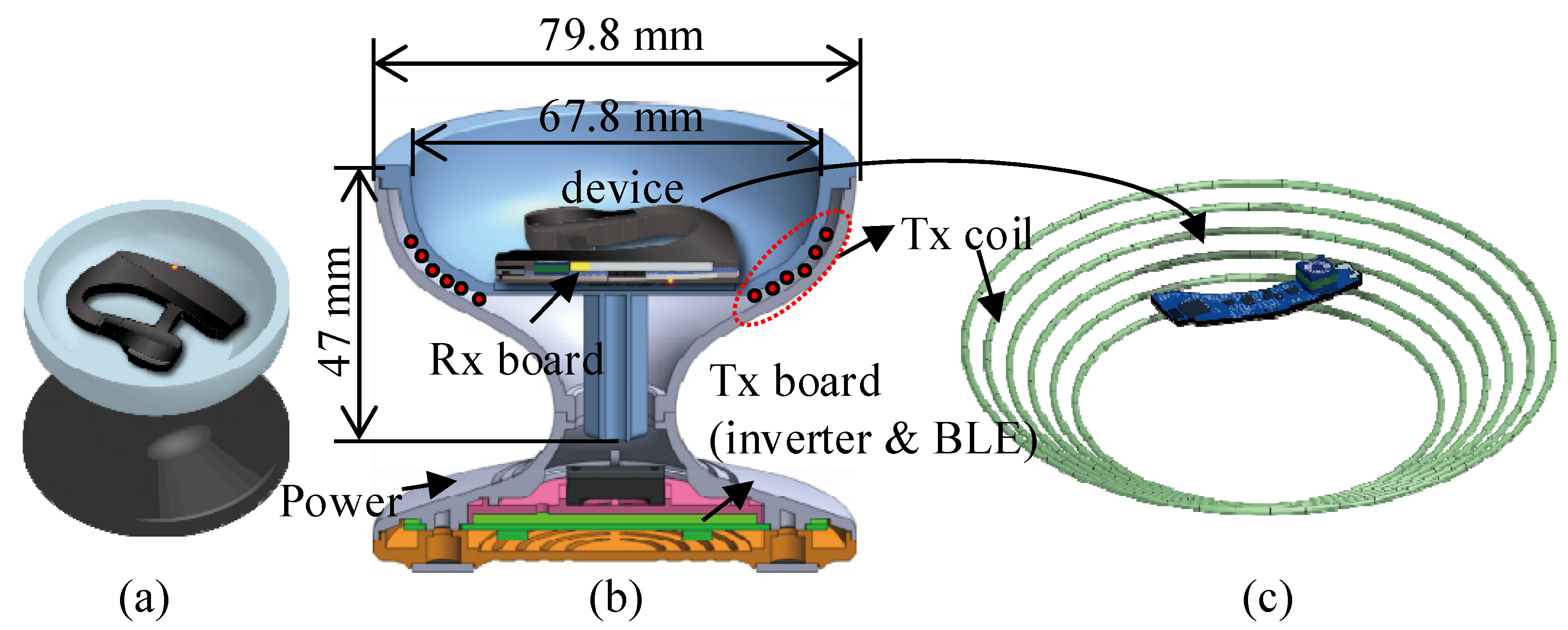
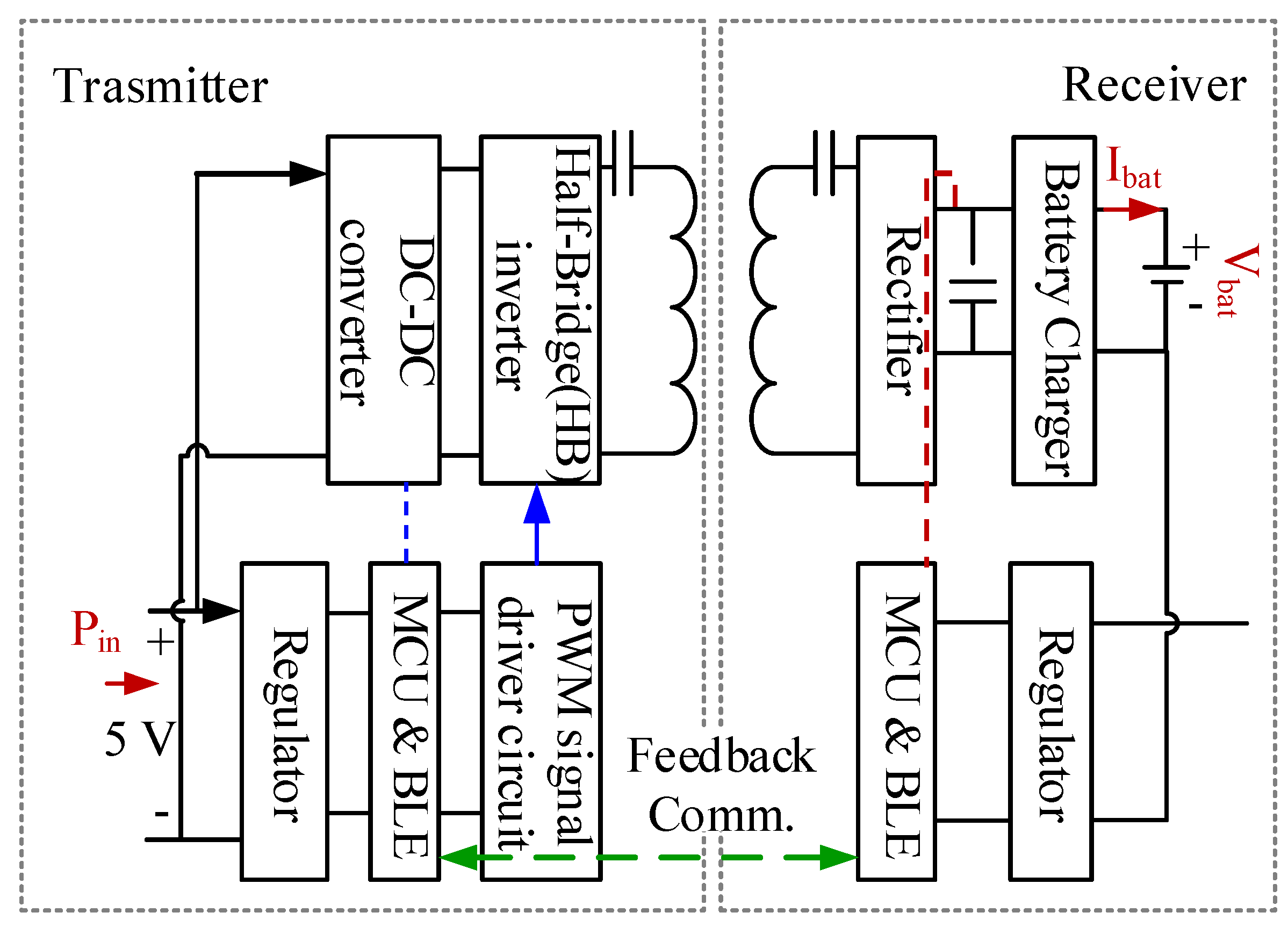
2. Proposed Wireless Power Transfer System for a Wearable Bio-Signal Monitoring Device

In Figure 1, the proposed wireless power transfer system is displayed. As shown in Figure 1b, a Tx circuit with a high-frequency inverter and Bluetooth low energy (BLE) module for charging control is placed at the base. As shown in Figure 1c, as a Tx coil, a bowl-shaped helix copper wire coil is used, which is equivalent to a concentric multi-loop helix coil. Therefore, the wearable bio-signal monitoring Rx device can be charged by simply placing it in the bowl. In addition, an Rx coil with a multilayer planar spiral coil is integrated with the printed circuit board (PCB) board of the device.
Figure 2a illustrates the double-layer and Figure 2b four-layer planar spiral coils that are used in the proposed system. The four-layer planar spiral coils are connected in series and consist of two PCBs. Each PCB has two spiral coils connected in series. The dielectric PCB substrate thickness is 0.6 mm, and the metal thickness is 2 oz. For the integration of the coil with a wearable bio-signal monitoring device, the maximum coil size is limited to 7 × 7 × 3.8 mm, with the distance between the two PCBs being 2.3 mm. The coil radius, RR, is 3 mm.

3. Calculation of Resistance and Inductance of the Multilayer Planar Spiral Coil

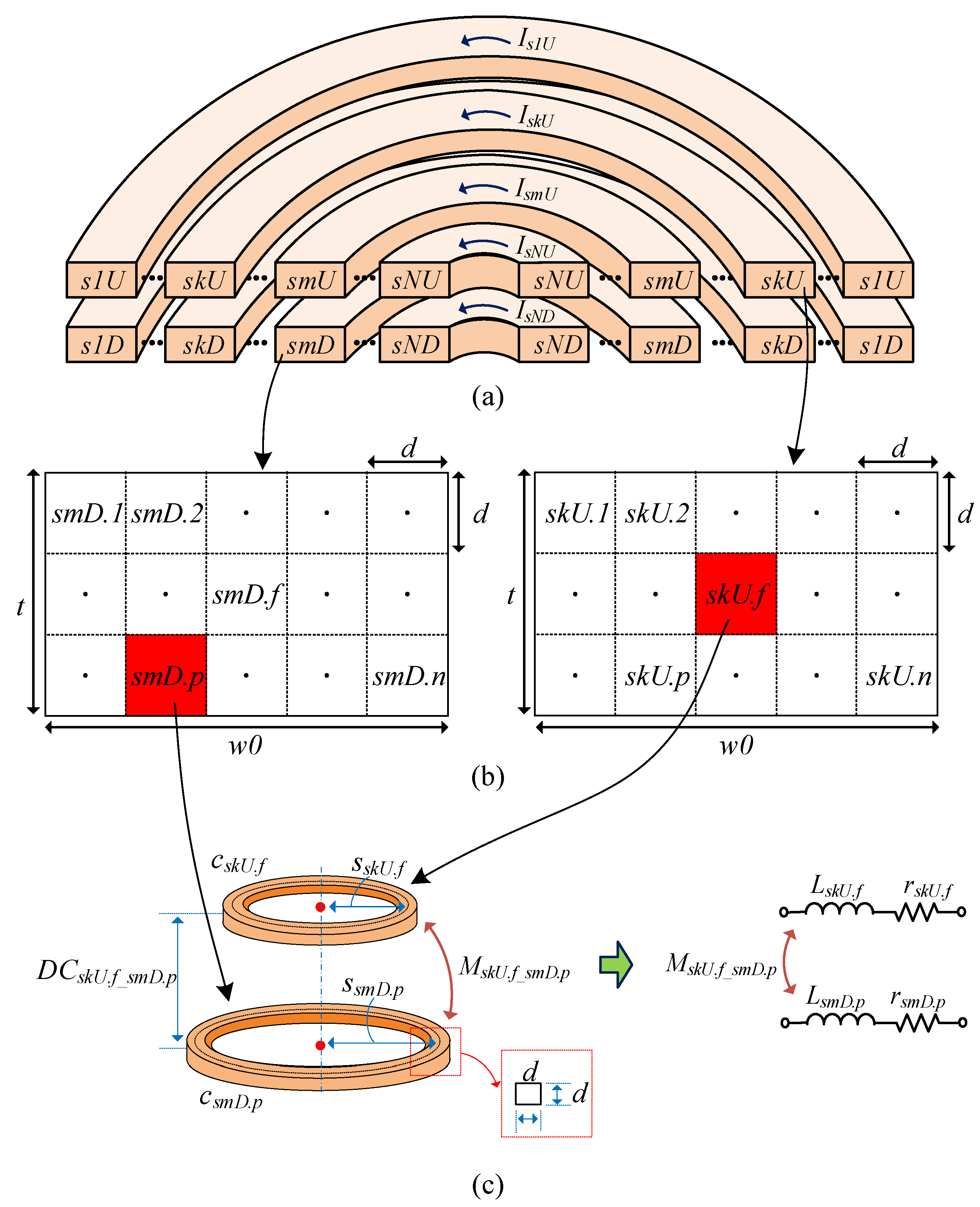
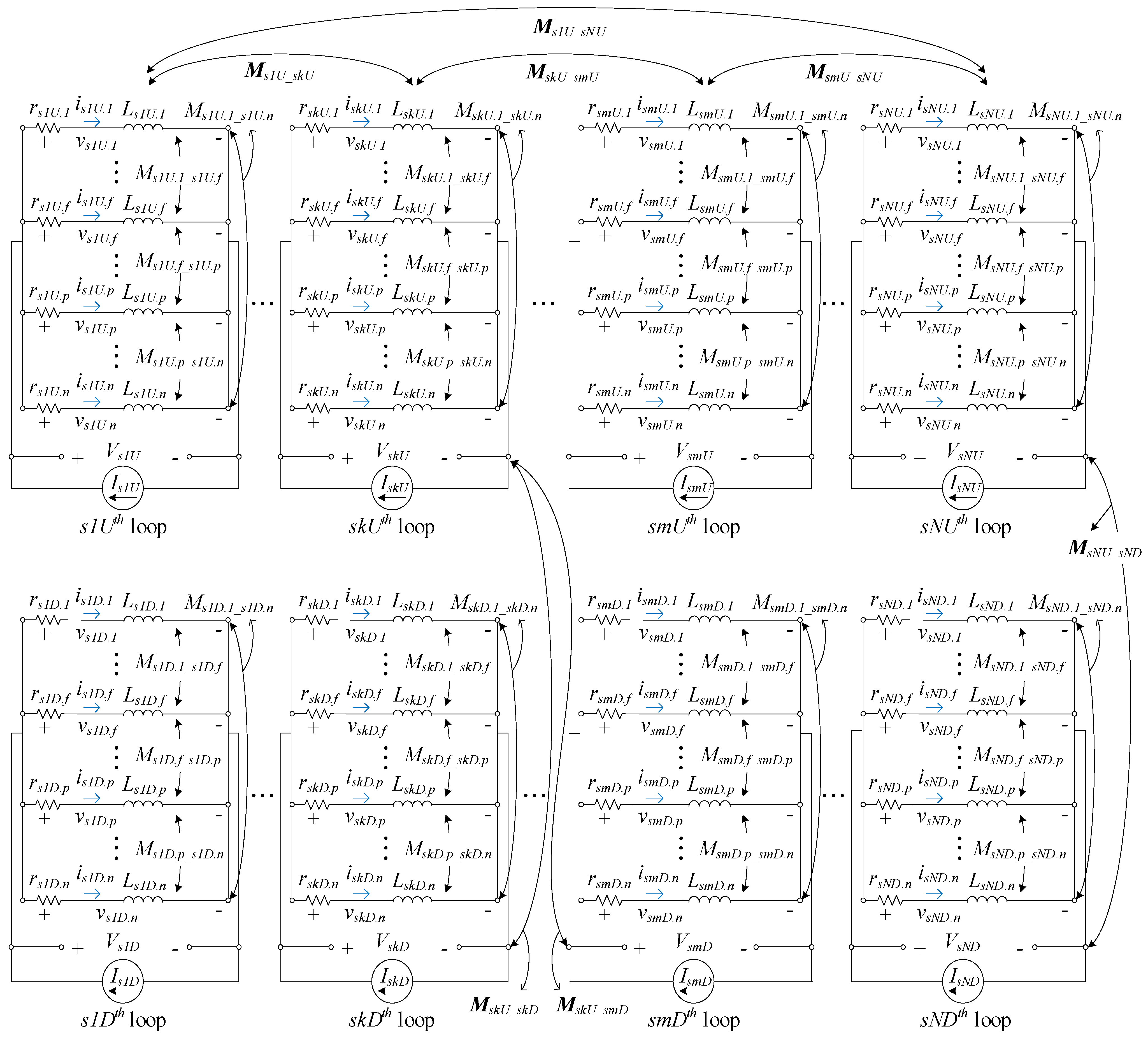
3.1. VFM and Equivalent Circuit Formulation for a Multilayer Planar Spiral Coil

In Figure 3a, the cross section of a n-loop planar coil is shown. It is noted that the n-loop double layer planar coil is equivalent to a double-layer planar spiral coil of n turns for simple calculation. The PCB thickness is T, the pattern width is w0, the gap is g, the metal thickness is t, and the turn number is n. The upper and bottom loops are aligned and connected in series, i.e., the kth loop has an upper loop, the skUth loop, and a bottom loop, the skDth loop. The net currents in each loop are identical.
For analysis, each loop is discretized into circular filament loops having a square cross section, with the square width, d, being less than 0.3δ, where δ is the skin depth, as shown in Figure 3b. In Figure 3b, the skUth and smDth loops are chosen. The number of the total mesh of each loop is n.
As shown in Figure 3c, two circular filament loops of the fth filament loop of the skUth loop, cskU.f, and the pth filament loop of the smDth loop, csmD.p, are chosen. MskU.f_smD.p is the mutual inductance between the two filament loops cskU.f and csmD.p. In addition, the two loops can be represented in terms of resistance (rskU.f, rsmD.p) and inductance (LskU.f, LsmD.p) of cskU.f and csmD.p and mutual inductance, as shown in Figure 3c.
In Figure 4, the equivalent circuit of the double-layer planar spiral coil of n turns that was used for analysis using the VFM is displayed. Each loop is represented with resistance and self-inductance of n filament loops, which are discretized in parallel. For example, the skUth and smDth loops in Figure 3 are represented with the equivalent circuits of skUth and smDth loops, which are equivalent to the resistance and inductance of n filament loops in Figure 4, respectively. Additionally, mutual inductances between two filament loops are included. For example, MskU.f_smU.p, MskU.f_smD.p, MskD.f_smU.p, and MskD.f_smD.p are the mutual inductances between two filament loops of cskU.f and csmU.p, cskU.f and csmD.p, cskD.f and csmU.p, and cskD.f and csmD.p, respectively. It should also be noted that the filament loop, cskU.f, is represented by resistance rskU.f and inductance LskU.f. Mutual inductances between two loops are represented in matrix form. For example, MskU_smU, MskU_smD, MskD_smU, and MskD_smD are the mutual inductance matrices between two loops of skUth and smUth, skUth and smDth, skDth and smUth, and skDth and smDth, respectively.
The net current of the skUth loop is IskU, and iskU.f is the current of the filament loop, cskU.f.
From the equivalent circuit, VskU is the voltage of the skUth loop and vskU.f is the voltage of the filament loop, cskU.f. Because each loop is connected in series,
V s k U = v s k U .1 = = v s k U . f = = v s k U . p = = v s k U . n .
By applying Kirchhoff’s voltage law to the circuit,
V T = X I T ,
where
V T = [ V s 1 V s k V s m V s N ] T ,
I T = [ I s 1 I s k I s m I s N ] T ,
V s k   = V s k U + V s k D ,   I s k = I s k U + I s k D ,
V s k U = [ v s k U . 1 v s k U . f v s k U . n ] ,   V s k D = [ v s k D . 1 v s k D . f v s k D . n ] ,
I s k U = [ i s k U .1 i s k U . f i s k U . n ] = I s k D = [ i s k D .1 i s k D . f i s k D . n ] ,
X = [ R s 1 + j ω M s 1 _ s 1 j ω M s 1 _ s k j ω M s 1 _ s m j ω M s 1 _ s N j ω M T s 1 _ s k R s k + j ω M s k _ s k j ω M s k _ s m j ω M s k _ s N j ω M T s 1 _ s m j ω M T s k _ s m R s m + j ω M s m _ s m j ω M s m _ s N j ω M T s 1 _ s N j ω M T s k _ s N j ω M T s m _ s N R s N + j ω M s N _ s N ]
Here, ω is the angular frequency and [∙]T is the transverse matrix of [∙]. The impedance matrix, X, consists of the resistance matrix and the mutual inductance matrix. The resistance matrix Rsk and the mutual inductance matrix Msk_sm are defined as follows:
R s k = [ R s k U 0 0 R s k D ] ,
M s k _ s m = [ M s k U _ s m U M s k U _ s m D M s k D _ s m U M s k D _ s m D ] ,
where
R s k U = [ r s k U . 1 0 0 0 0 r s k U . f 0 0 0 0 r s k U . p 0 0 0 0 r s k U . n ] ,
R s k D = [ r s k D . 1 0 0 0 0 r s k D . f 0 0 0 0 r s k D . p 0 0 0 0 r s k D . n ] ,
M s k U _ s m U = [ M s k U .1 _ s m U .1 M s k U .1 _ s m U . f M s k U .1 _ s m U . p M s k U .1 _ s m U . n M s k U . f _ s m U .1 M s k U . f _ s m U . f M s k U . f _ s m U . p M s k U . f _ s m U . n M s k U . p _ s m U .1 M s k U . p _ s m U . f M s k U . p _ s m U . p M s k U . p _ s m U . n M s k U . n _ s m U .1 M s k U . n _ s m U . f M s k U . p _ s m U . p M s k U . n _ s m U . n ] ,
M s k U _ s m D = [ M s k U .1 _ s m D .1 M s k U .1 _ s m D . f M s k U .1 _ s m D . p M s k U .1 _ s m D . n M s k U . f _ s m D .1 M s k U . f _ s m D . f M s k U . f _ s m D . p M s k U . f _ s m D . n M s k U . p _ s m D .1 M s k U . p _ s m D . f M s k U . p _ s m D . p M s k U . p _ s m D . n M s k U . n _ s m D .1 M s k U . n _ s m D . f M s k U . p _ s m D . p M s k U . n _ s m D . n ] ,
M s k D _ s m U = [ M s k D .1 _ s m U .1 M s k D .1 _ s m U . f M s k D .1 _ s m U . p M s k D .1 _ s m U . n M s k D . f _ s m U .1 M s k D . f _ s m U . f M s k D . f _ s m U . p M s k D . f _ s m U . n M s k D . p _ s m U .1 M s k D . p _ s m U . f M s k D . p _ s m U . p M s k D . p _ s m U . n M s k D . n _ s m U .1 M s k D . n _ s m U . f M s k D . p _ s m U . p M s k D . n _ s m U . n ] ,
M s k D _ s m D = [ M s k D .1 _ s m D .1 M s k D .1 _ s m D . f M s k D .1 _ s m D . p M s k D .1 _ s m D . n M s k D . f _ s m D .1 M s k D . f _ s m D . f M s k D . f _ s m D . p M s k D . f _ s m D . n M s k D . p _ s m D .1 M s k D . p _ s m D . f M s k D . p _ s m D . p M s k D . p _ s m D . n M s k D . n _ s m D .1 M s k D . n _ s m D . f M s k D . p _ s m D . p M s k D . n _ s m D . n ] ,
RskU and RskD are the diagonal matrices of the resistance of n filament loops of the skUth and skDth loops, as shown in Figure 4, respectively. MskU_smU, MskU_smD, MskD_smU, and MskD_smD are the matrixes of MskU.f_smU.p, MskU.f_smD.p, MskD.f_smU.p, and MskD.f_smD.p with k, m = 1, ∙∙∙, n and f, p = 1, ∙∙∙, n, respectively. When k = m and f = p, MskU.f_smU.p and MskD.f_smD.p become the self-inductances of cskU.f, LskU.f, and cskD.f, LskD.f, respectively.
The current distribution of each filament loop can be assumed to be uniform [12]; thus, the resistance of cskU.f, rskU.f, can be written as follows:
r s k U . f = 2 π s s k U . f σ d 2 ,
where σ is the conductivity of copper.
The inductance of cskU.f, LskU.f, is calculated as follows:
L s k U . f = μ 0 s s k U . f [ ln 8 s s k U . f ( d / 2 ) 1.75 ] .
Here, μ0 is the permeability in vacuum.
The mutual inductance, MskU.f_smD.p, is given by the following equation:
M s k U . f _ s m D . p = μ 0 s s k U . f s s m D . p [ ( 2 κ 2 ) Κ ( κ ) 2 κ Ε ( κ ) ] ,
where
κ = 4 s s k U . f s s m D . p ( s s k U . f 2 + s s m D . p 2 ) + ( D C s k U . f _ s m D . p ) 2 .
K(κ) and E(κ) are the complete elliptic integrals of the first and second kind, respectively [13].
From the equivalent circuit, the net currents of the loops are identical and can be expressed as follows:
I s 1 U = I s 1 D = = I s k U = I s k D = = I s N U = I s N D ,
where
I s k U = f = 1 n i s k U . f ,     I s k D = f = 1 n i s k D . f .
Therefore, VT and IT can be written as follows:
V T = F s 1 U T V s 1 U + F s 1 D T V s 1 D + + F s k U T V s k U + + F s N D T V s N D ,
I T = F s 1 U T I s 1 U + F s 1 D T I s 1 D + + F s k U T I s k U + + F s N D T I s N D ,
where
F s k U , D = [ 1 n T δ s 1 U _ s k U 1 n T δ s 1 D _ s k D 1 n T δ s m U _ s k U 1 n T δ s N D _ s k D ] ,
δ s m U / D _ s k U / D = { 1 ;   m = k 0 ;   o t h e r w i s e .
[ V s 1 U V s 1 D V s k U V s N D ] = [ F s 1 U X 1 F s 1 U T F s 1 U X 1 F s 1 D T F s 1 U X 1 F s k U T F s 1 U X 1 F s N D T F s 1 D X 1 F s 1 U T F s 1 D X 1 F s 1 D T F s 1 D X 1 F s k U T F s 1 D X 1 F s N D T F s k U X 1 F s 1 U T F s k U X 1 F s 1 D T F s k U X 1 F s k U T F s k U X 1 F s N D T F s N D X 1 F s 1 U T F s N D X 1 F s 1 D T F s N D X 1 F s k U T F s N D X 1 F s N D T ] [ I s 1 U I s 1 D I s k U I s N D ]
From the equivalent circuit, the voltage of the kth loop, Vsk, is the sum of the voltage of the skUth loop, VskU, and the voltage of the skDth loop, VskD, and is expressed as follows:
V sk = V skU + V skD ,
where
V s k U = [ v s k U .1 v s k U . f v s k U . n ] ,     V s k D = [ v s k D .1 v s k D . f v s k D . n ] .
If a current of 1 A flows through the coil, the total voltage across the coil equals the coil impedance. Therefore, the resistance, R, and inductance, L, of the coil can be written as follows:
R = R e ( k = 1 N ( V s k U + V s k D ) ) ,
L = 1 ω I m ( k = 1 N ( V s k U + V s k D ) ) .
Re(∙) and Im(∙) are the real and imaginary parts of (∙), respectively.

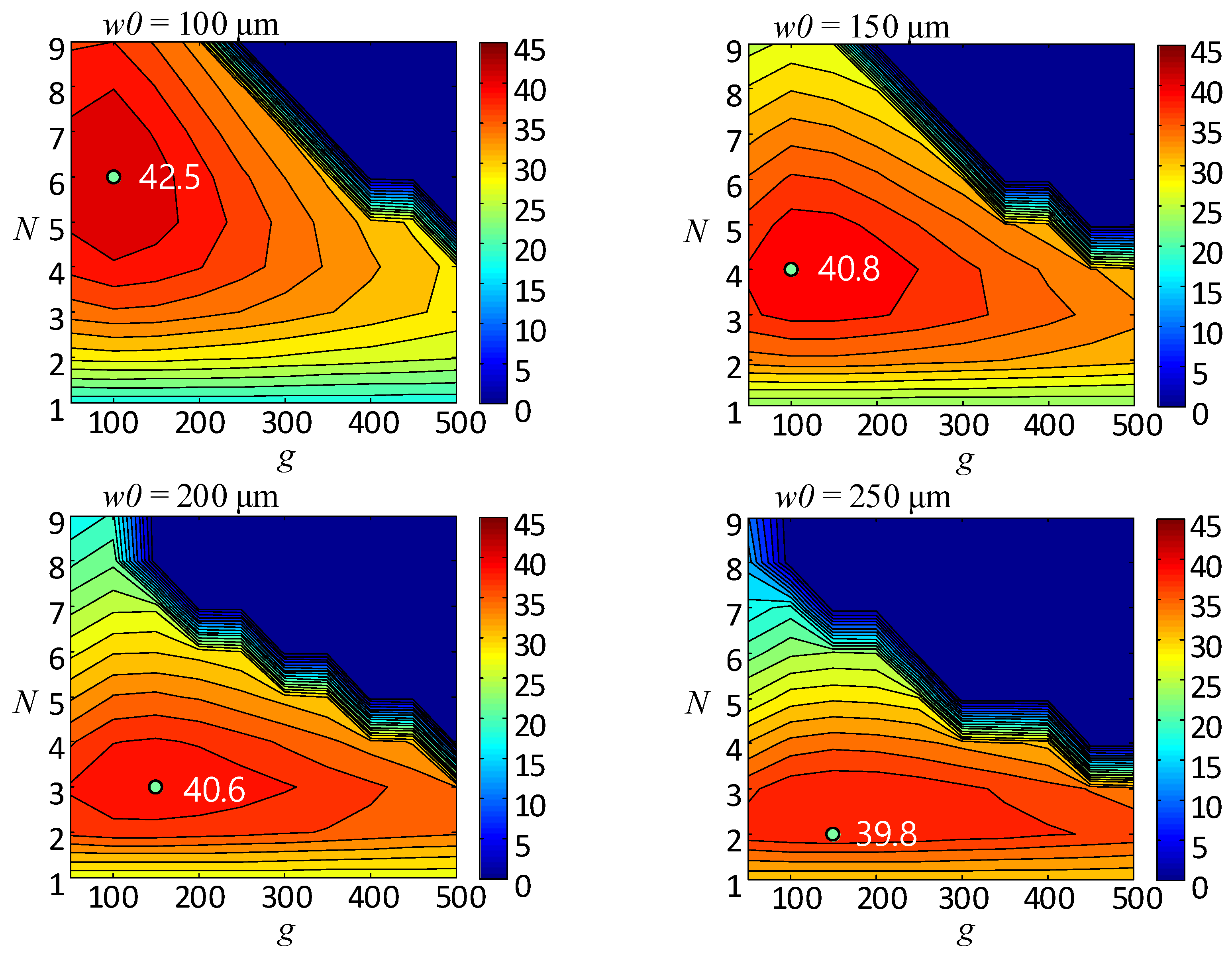
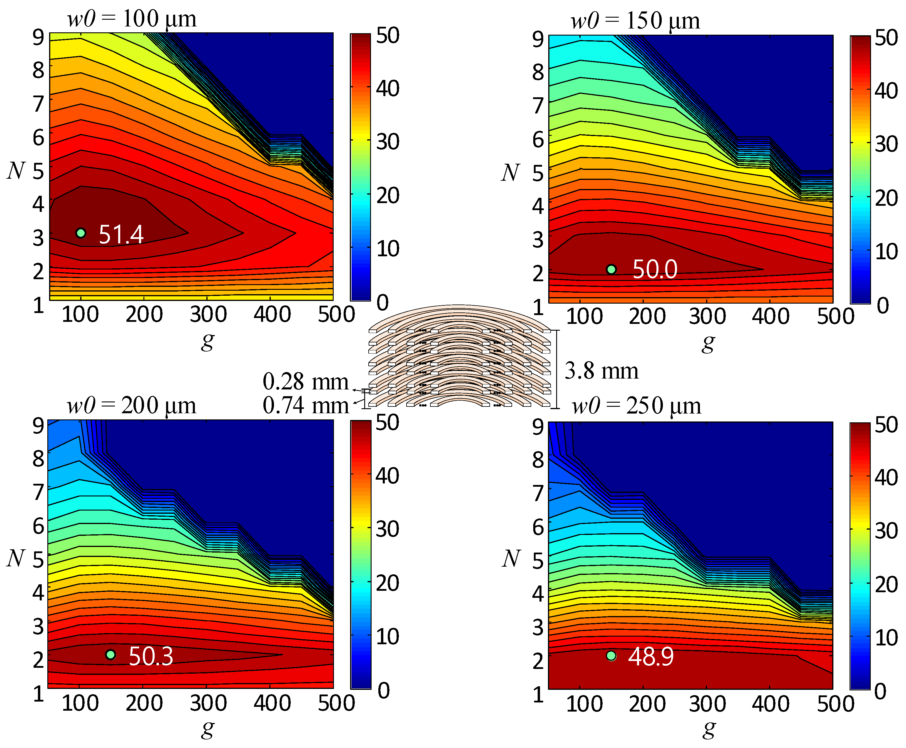
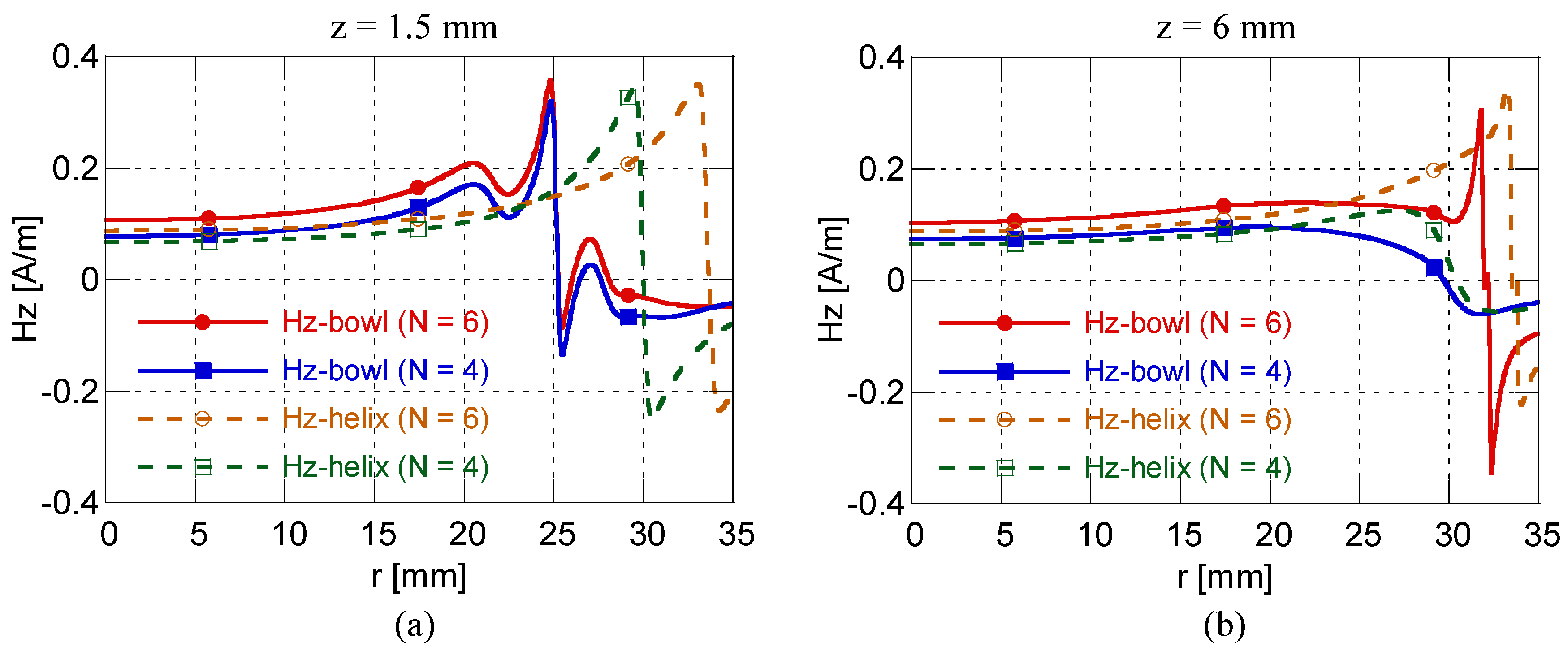
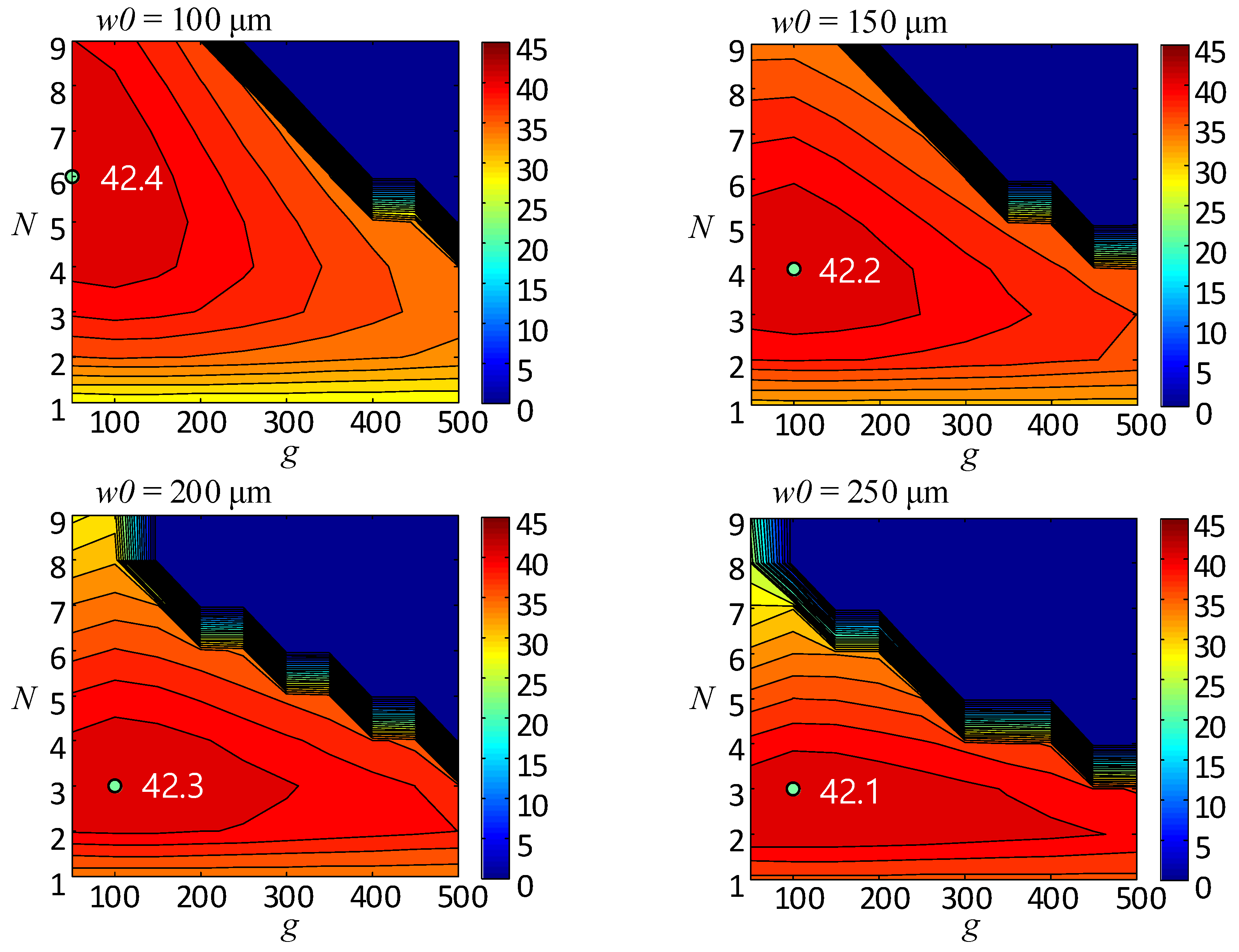
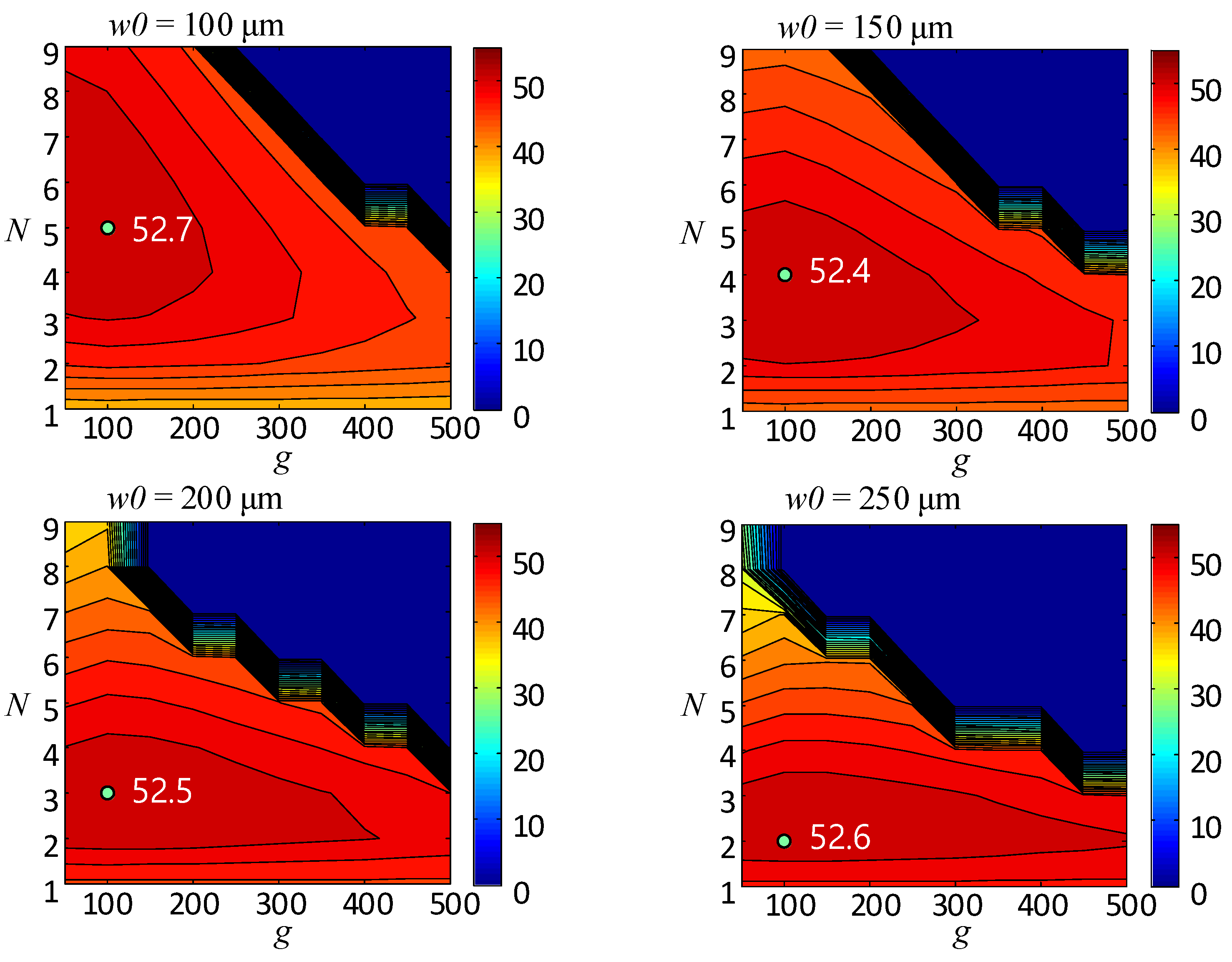
3.2. Calculation Results and Analysis

For the verification of the proposed method, the calculation results were compared with the results of the simulation using ANSYS Maxwell. For calculation, the multilayer planar spiral coils are considered to be equivalent to the concentric multiloop coil, as shown in Figure 2, and t = 2 oz (~70 μm), T = 0.6 mm, and w0 = 0.15 mm are used. In Figure 5, the change in resistance and inductance with n are compared with the simulation results for double-layer and four-layer planar spiral coils with g = 0.15 mm. The calculation results are in good agreement with the simulation. In Figure 5c, the Q-factor of the calculation and simulation are displayed for the four-layer planar spiral coil. The Q-factor is obtained using the resistance and inductance of the coils as follows, where Q-factor = ωL/R. R and L are used in Figure 5b. It should be noted that the optimal n can be determined for the maximum Q-factor because as n increases up to n = 4, the increase ratio of inductance is higher than that of resistance. In addition, it should be noted that for N greater than or equal to 5, the increase ratio of inductance reduces although that of resistance continues to increase, because the proximity effect rapidly increases; a similar trend is observed in the case of planar square coils [6]. The inductance and resistance of the four-layer planar spiral coil are more than double those of the double-layer planar spiral coil.
In Figure 6, the calculations of resistance and inductance according to the gap g between two neighboring patterns are compared with simulated values for double-layer and four-layer planar spiral coils for N = 4. As shown, the calculation is in good agreement with the simulation. It is clear that the resistance and inductance decrease with increasing g. In Figure 6c, the calculation and simulation of Q-factor are displayed for four-layer planar spiral coils. The optimal gap dimension can be determined for the maximum Q-factor because, as g increases up to g = 0.15 mm, the increase ratio of inductance is higher than that of resistance. The inductance and resistance of the four-layer planar spiral coil are more than double those of double-layer planar spiral coil.
Figure 7 shows the calculated Q-factor according to g and N for the double-layer planar spiral coil with various w0. The optimal N and g for each w0 can be obtained for the maximum Q-factor. The maximum Q-factor is 39.5 (L = 939.42 nH, R = 1013.37 mΩ) for w0 = 100 μm, N = 7, and g = 100 μm. From the color bar, dark red represents a higher Q-factor. In the area of dark blue, coils cannot be made with the coil dimension.
Figure 8 shows the calculated Q-factors according to g and N for the four-layer planar spiral coil. The maximum Q-factor is 42.5 (L = 1802.8 nH, R = 1811.5 mΩ) for w0 = 100 μm, N = 6, and g = 100 μm. In addition, the maximum Q-factors for w0 = 150 μm, w0 = 200 μm, and w0 = 250 μm are 40.8 (L = 896.8 nH, R = 935.4 mΩ), 40.6 (L = 500.89 nH, R = 526.16 mΩ), and 39.8 (L = 258.52 nH, R = 276.45 mΩ), respectively. It is noted that as w0 increases, the optimal N and coil inductance for the maximum Q-factor decrease, whereas the maximum Q-factors are similar regardless of w0.
Figure 9 shows the calculated Q-factors according to g and N for the eight-layer planar spiral coil. The maximum Q-factor is 51.4 (L = 2428.0 nH, R = 2.01 Ω) for w0 = 100 μm, N = 3, and g = 100 μm.
From Figure 7, Figure 8 and Figure 9, the eight-layer planar spiral coil has the highest maximum Q-factor, compared with the double- and four-layer planar spiral coils. This is because the increase in the inductance is higher than that of the resistance at optimal N and g with the increase in the number of coil layers. As the number of coil layers increases up to eight layers, the maximum Q-factors increase, whereas the optimal turn number decreases. In addition, it is shown that the maximum Q-factors are similar regardless of w0 for each layer, whereas the optimal dimensions for the maximum Q-factor vary in relation to w0.
Because the optimal dimensions required for the maximum Q-factor may differ from those required for the maximum coupling efficiency, the maximum coupling efficiency according to g and N for double-, four-, and eight-layer planar spiral coils with various w0 are calculated. The maximum coupling efficiency, η, can be calculated as follows [14,15]:
η = FoM 2 ( 1 + FoM 2 + 1 ) 2 = 1 + FoM 2 1 1 + FoM 2 + 1   with   FoM = ω M Tx Rx R Tx · R Rx .
RTx and RRx are the resistances of the Tx and Rx coils, respectively. MTx-Rx is the mutual inductance between the Tx and Rx coils. FoM stands for the Figure of Merit of the MR-WPT system.
In Figure 10, the cross-sectional and top views of the Tx coil and four-layer Rx coil for calculation are shown. The Rx coil is placed in the middle of Tx coil, and the bottom of the Rx coil is placed slightly higher than z = 1.2 mm because a practical bowl will have a finite thickness of about 1 mm.
As shown in Figure 10, the bowl-shaped coil of six turns was designed by referring to [16]. It is advantageous to obtain a smaller skin resistance when the diameter of the copper wire is larger than the skin depth of 6.78 MHz, whereas the bowl-shaped coil has a higher magnetic field than the helix coil. The four-turn coils have lower magnetic fields than the six-turn coils.
For a high and uniform magnetic field between z = 1.5 mm and z = 6 mm in the bowl, the Tx coil was designed. It can be noted that a four-layer Rx coil will be placed between z = 1.5 mm and z = 6 mm in the bowl. By using the calculation equations in [16], for a z-directed magnetic field, Hz is calculated. In Figure 11a, the calculated magnetic fields at z = 1.5 and Figure 11b z = 6 mm are displayed. In addition, the calculation results of helix coils are compared with the bowl-shaped coils for four- and six-turn coils. For the case of four turns, two turns from the top are removed. Both Tx and helix coils of six turns for z = 1.5 mm and 6 mm have a uniform magnetic field in the charging area from r = 0 to r = 20 mm, whereas the bowl-shaped coil has a higher magnetic field than the helix coil. The four-turn coils have lower magnetic fields than the six-turn coils.
Figure 12, Figure 13 and Figure 14 show the calculated maximum coupling efficiency (%) according to g and N for double-layer, four-layer, and eight-layer planar spiral coils with w0 = 100, 150, 200, and 250 μm. As shown, the optimal N and g for each w0 was found to obtain the maximum coupling efficiency. The dimensions for the maximum coupling efficiency are similar to those for the maximum Q-factor, except for those for w0 = 100 μm. Further, the maximum coupling efficiency increases with more layers, up to eight layers, whereas maximum coupling efficiencies for each layer are similar regardless of w0. It is noted that optimal coil dimensions for each layer should be found for maximum coupling efficiency.
It is shown that the eight-layer planar spiral coil has the highest maximum coupling efficiency. This is because the Q-factor for the eight-layer coil is the highest of the double-, four-, and eight-layer coils, as shown in Figure 7, Figure 8 and Figure 9. Additionally, the mutual inductance between the Tx coil and Rx coil for the eight-layer planar spiral coil is the highest.
Based on the findings from Figure 12, Figure 13 and Figure 14, N = 4, w0 = 150 μm, and g = 200 μm for a four-layer planar spiral coil were chosen as the optimal values for the device by considering easy fabrication, reasonable manufacturing cost, and easy integration with the main PCB board. Moreover, from the practical viewpoint, it is more advantageous to design a coil of higher inductance for small WPT systems. That is, for the maximum Q-factor for the four-layer coil, L = 896.8 nH for w0 = 150 μm is higher than those of L = 500.89 nH for w0 = 200 μm and L = 258.52 nH for w0 = 250 μm.

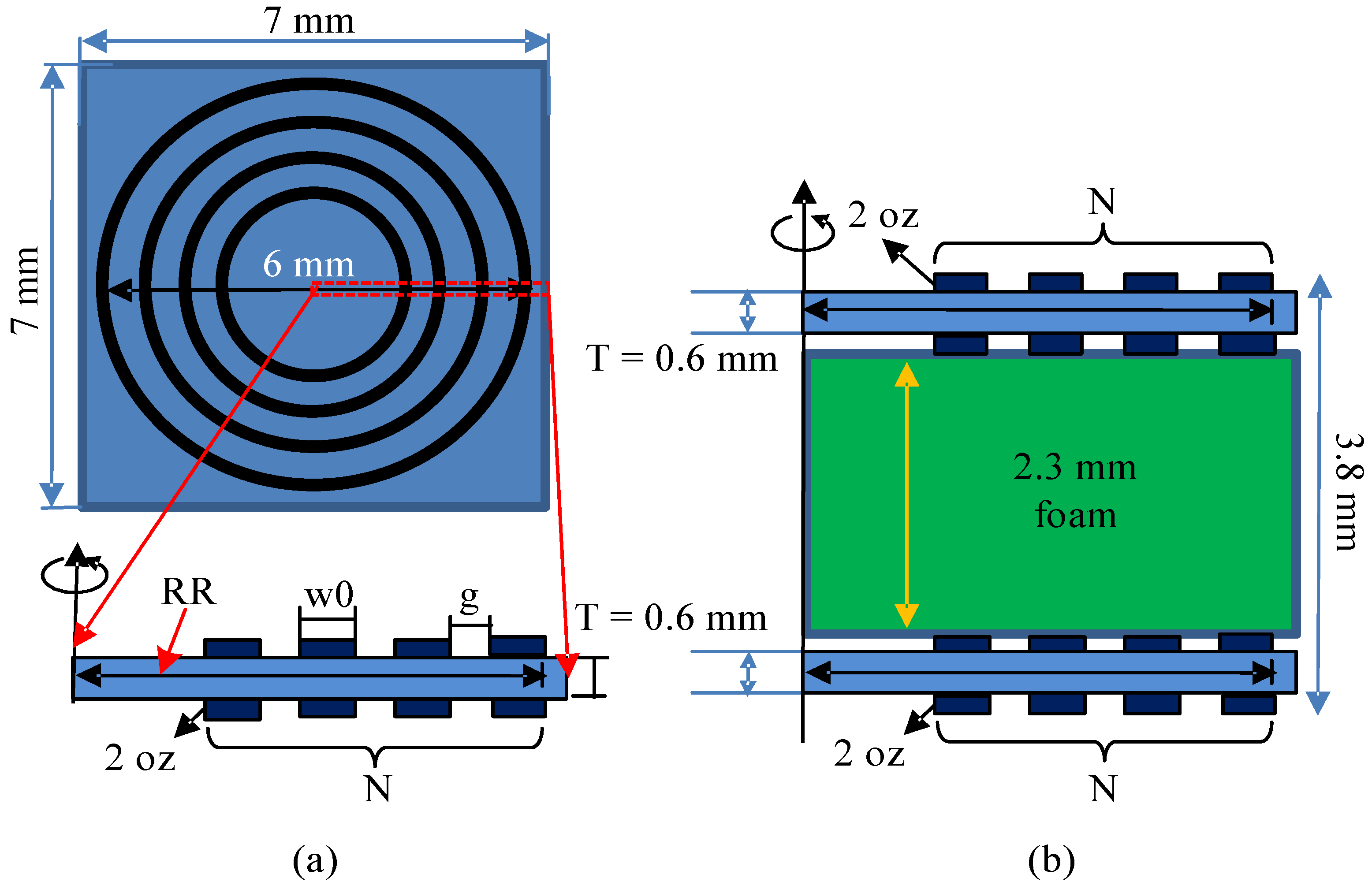
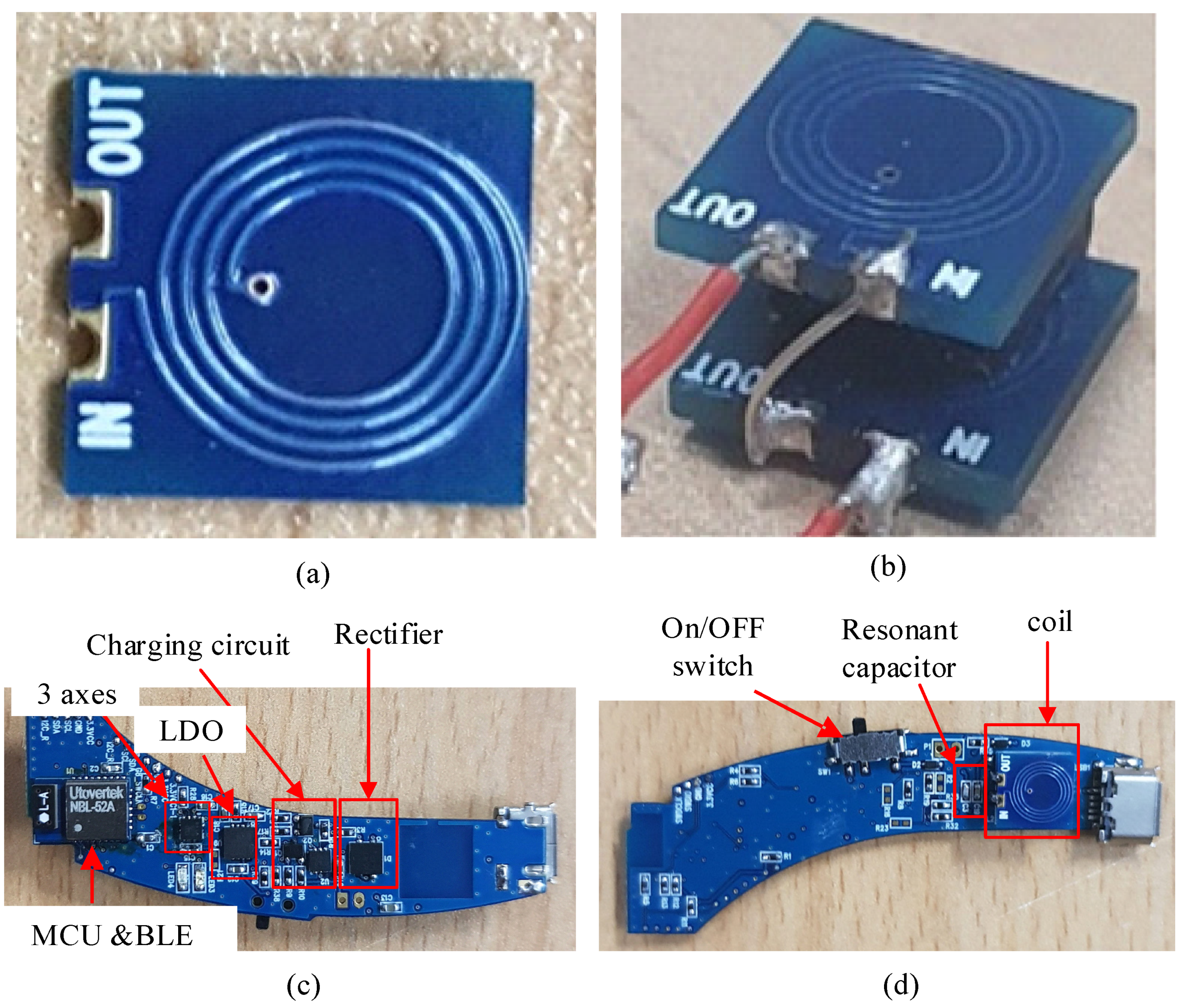
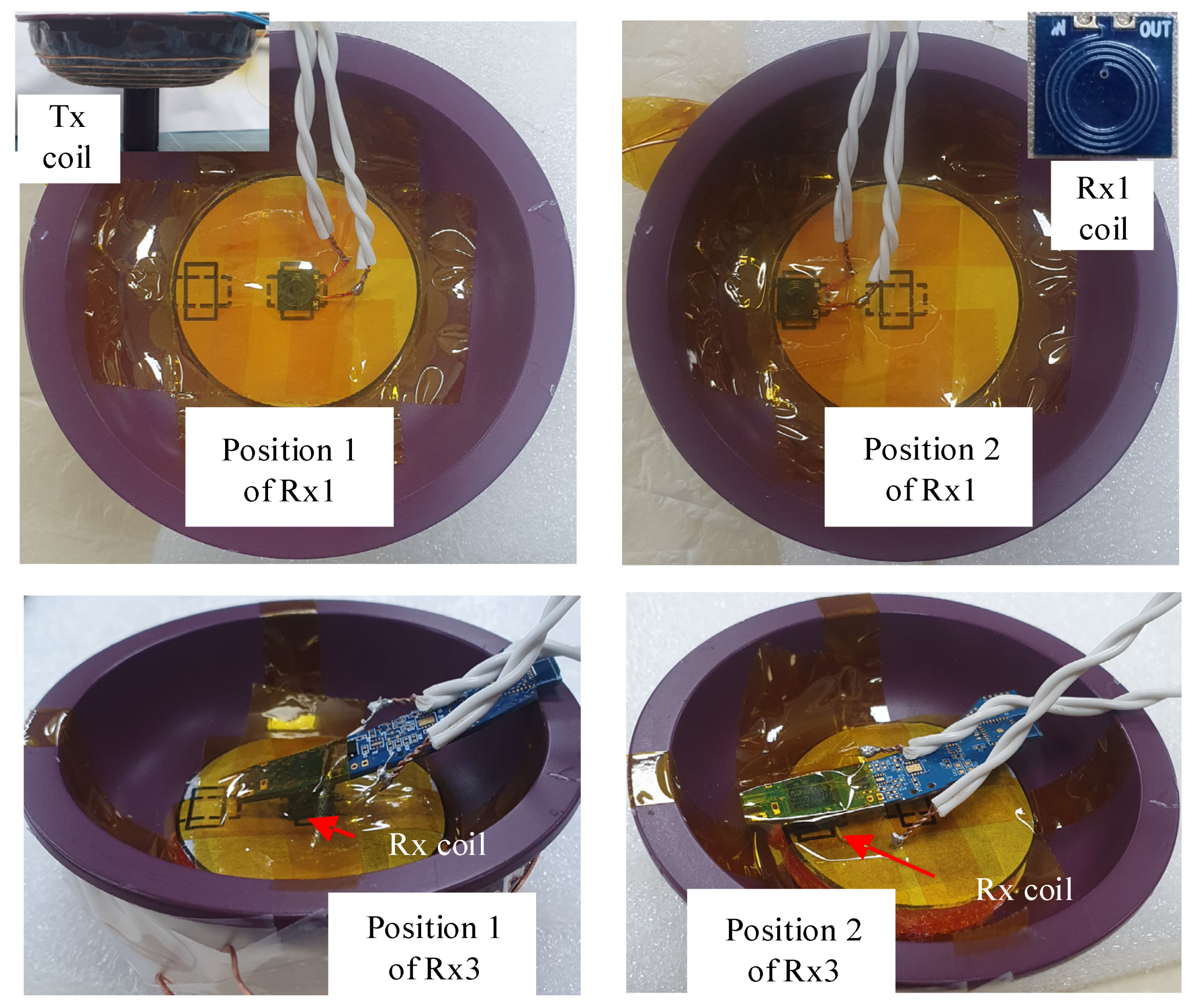
4. Coil Fabrication and Measurement

A four-layer planar spiral coil was fabricated using the calculated parametric values. The four-layer planar spiral coil was made by connecting two double-layer planar spiral coils in series. Figure 15a shows a top view of a double-layer planar spiral coil. The coil specification is N = 4, w0 = 150 μm, g = 200 μm, t = 2 oz, radius of outmost loop RR = 3.0 mm, and T = 0.6 mm. In Figure 15b, the fabricated four-layer planar spiral coil is displayed. The distance between two double-layer planar spiral coils is 2.3 mm. Figure 15c shows the PCB of the bio-signal monitoring device. Figure 15d shows the back view of the circuit board of the four-layer planar spiral coil.
Figure 16 shows the measurement setup. Rx1 is a double-layer planar spiral coil as shown in Figure 15a. Rx2, shown in Figure 15b, is a four-layer planar spiral coil. Position 1 is in the middle of the Tx coil and position 2 is at the border of the glass. Rx3 is a four-layer planar spiral coil on the Rx board. For the measurement of resistance, inductance, and mutual inductance, the Agilent E5072A network analyzer was used.
The fabricated Tx coil is shown in the inset of the upper-left figure shown in Figure 16. The Tx coil was also measured, and the inductance and AC resistance were 3.0322 μH and 429.15 mΩ, respectively.
Table 1 lists the measurement results, with the calculation results for comparison. Inductance, resistance, and mutual inductance measurements are shown in the table. The measurements of FoM and maximum coupling efficiency in the table were obtained using Equation (15), and the resistance, inductance, and mutual inductance were measured. The measured resistance and inductance are in good agreement with the calculated values. However, the resistance values slightly differ because the coil pattern of the fabricated device is slightly narrower for w0 = 130 μm, in comparison with the designed value of 150 μm. Moreover, the maximum coupling efficiency is obtained at the edge because the mutual inductance at position 2 is higher than that at position 1, as shown in Table 1.

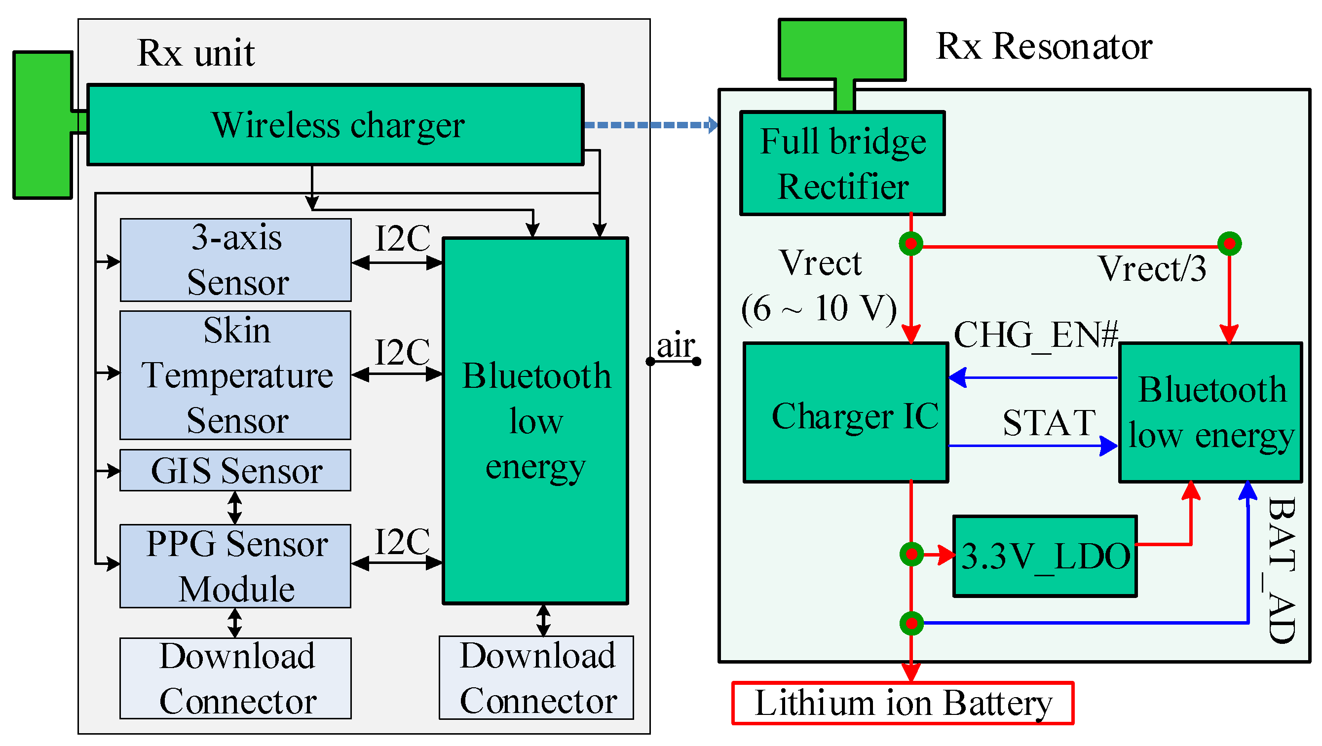
5. Wearable Bio-Signal Monitoring Device and Wireless Charging

Figure 17 shows a block diagram of the proposed MR-WPT system for biomedical devices. For the Tx system, the Tx circuit in [17] was used.
In Figure 18, a block diagram of a bio-signal monitoring device and wireless charging station are shown. The device comprises a wireless charger, BLE for the communication of the sensor data, a wireless charging control station, a three axis sensor, a skin temperature sensor (in-ear), a geographic information systems (GIS) sensor, and a photoplethysmography (PPG) sensor (in ear). The wireless charger is designed with two power stages, which consist of a full bridge rectifier (SBR05M100BLP), charger IC (MCP73830L), and LDO (LT3802EDD) to minimize the power conversion efficiency.
Figure 19 shows the experimental setup. A KEITHLEY 2280S-60-3 was used for the power supply, and the KEITHLEY 2280S-60-3 as a battery simulator was used for the battery charging experiment. The total power to the Tx board was about 1.3 W (5 V/0.26 A), which includes the power consumption for BLE communication. The measured Rx power of the battery simulator was 0.209 mW (4.152 V/50.4 mA). Therefore, the wireless power transfer efficiency from the Tx board to Rx battery was 16.08%. The power conversion efficiency for the Tx and Rx circuits can be improved, especially for the low-power applications of wearable devices.
Finally, this work is compared with previous works in Table 2. As shown, the coil in the paper is the smallest multilayer planar spiral coil for MR-WPT applications at 6.78 MHz. In addition, the dc-dc efficiency of this work is higher than that in [7], in which a helix Tx coil and a double-layer planar spiral Rx coil were used.

6. Conclusions

This study analyzed multilayer planar spiral coils applied to MR-WPT in the MHz frequency range for use in compact wearable bio-signal monitoring devices using the VFM. In the current paper, the calculation method for the AC resistance and inductance using the VFM is explained in detail. Moreover, the planar spiral coil can be optimized to obtain the maximum Q-factor and maximum coupling efficiency using the calculation. As the number of layers of coils increases, the maximum Q-factor and maximum coupling efficiency increase, up to a total of eight layers, when the coils are optimized using the proposed method. The calculation method was verified via simulations and measurements. It is shown that the proposed method is able to analyze the AC resistance and inductance inclusive of the proximity loss and skin effects in the MHz frequency range. Finally, a four-layer planar spiral coil was designed using the proposed optimization method to be used for wireless charging of a compact wearable bio-signal monitoring device. To the best of the authors’ knowledge, the proposed device is the smallest multilayer planar spiral coil for MR-WPT application at 6.78 MHz. In addition, the optimization process of multiple layer planar spiral coils is shown for the maximum Q-factor and maximum coupling efficiency. The proposed method is applicable to the optimization of planar spiral coils for use in mobile devices.

Author Contributions

Conceptualization, Y.-J.P.; methodology, Y.-J.P. and J.-E.K.; validation, J.-E.K., K.-M.N., K.-D.Y. and K.-H.C.; formal analysis, Y.-J.P. and J.-E.K.; investigation, Y.-J.P.; resources, Y.-J.P.; data curation, J.-E.K. and K.-M.N.; writing—original draft preparation, Y.-J.P.; writing—review and editing, Y.-J.P. and J.-E.K.; visualization, J.-E.K.; supervision, Y.-J.P.; project administration, Y.-J.P.; funding acquisition, Y.-J.P. All authors have read and agreed to the published version of the manuscript.

Funding

This research was funded by the KERI Primary research program of MSIT/NST, grant number 21A01033 and the Industrial Infrastructure Program for Fundamental Technologies of KIAT, grant number P0014854 (21A02059), and the Ministry of Trade, Industry and Energy (MOTIE), Korea.

Data Availability Statement

Not applicable.

Conflicts of Interest

The authors declare no conflict of interest.

References

  1. Won, S.M.; Song, E.; Reeder, E.T.; Rogers, J.A. Emerging Modalities and Implantable Technologies for Neuromodulation. Cell 2020, 181, 115–135. [Google Scholar] [CrossRef]
  2. Won, S.M.; Cai, L.; Gutruf, P.; Rogers, J.A. Wireless and battery-free technology for neuroengineering. Nat. Biomed. Eng. 2021, 1–19. [Google Scholar] [CrossRef]
  3. Jeong, S.; Kim, D.; Song, J.; Kim, H.; Lee, S.; Song, C.; Lee, J.; Song, J.; Kim, J. Smartwatch strap wireless power transfer system with flexible PCB coil and shielding material. IEEE Trans. Ind. Electron. 2019, 66, 4054–4064. [Google Scholar] [CrossRef]
  4. Wagih, M.; Komolafe, A.; Zaghari, B. Wearable Wireless Power Transfer using Direct-Write Dispenser Printed Flexible Coils. In Proceedings of the 2020 IEEE International Conference on Flexible and Printable Sensors and Systems (FLEPS), Manchester, UK, 16–19 August 2020; pp. 1–4. [Google Scholar] [CrossRef]
  5. Jow, U.-M.; Ghovanloo, M. Design and Optimization of Printed Spiral Coils for Efficient Transcutaneous Inductive Power Transmission. IEEE Trans. Biomed. Circuits Syst. 2007, 1, 193–202. [Google Scholar] [CrossRef] [PubMed]
  6. Kim, D.-H.; Park, Y.-J. Calculation of the inductance and AC resistance of planar rectangular coils. Electron. Lett. 2016, 52, 1321–1323. [Google Scholar] [CrossRef]
  7. Kim, C.Y.; Ku, M.J.; Qazi, R.; Nam, H.J.; Park, J.W.; Nam, K.S.; Oh, S.; Kang, I.; Jang, J.-H.; Kim, W.Y.; et al. Soft subdermal implant capable of wireless battery charging and programmable controls for applications in optogentics. Nat. Commun. 2021, 12, 535. [Google Scholar] [CrossRef] [PubMed]
  8. Lope, I.; Carretero, C.; Acero, J.; Alonso, R.; Burdio, J.M. AC Power Losses Model for Planar Windings With Rectangular Cross-Sectional Conductors. IEEE Trans. Pow. Electron. 2014, 29, 23–28. [Google Scholar] [CrossRef]
  9. Chen, K.; Zhao, Z. Analysis of the Double-Layer Printed Spiral Coil for Wireless Power Transfer. IEEE Trans. Emerg. Sel. Topics Power Electron. 2013, 1, 114–121. [Google Scholar] [CrossRef]
  10. Gong, F.; Cong, Y.; Wei, Z.; Yin, B.; Chi, H.; Luan, X. Analysis of the multi-layer Printed Spiral Coil for wireless power transfer system used in medical implants. 2016 Asia-Pacific Int. Symp. Electromag. Comp. (APEMC) 2016, 1, 460–462. [Google Scholar] [CrossRef]
  11. Bao, K.; Zekios, C.L.; Georgakopoulos, S.V. A wearable WPT system on flexible substrates. IEEE Antennas Wireless Propag. Lett. 2019, 18, 931–935. [Google Scholar] [CrossRef]
  12. Kim, D.-H.; Kim, J.; Park, Y.-J. Optimization and Design of Small Circular Coils in a Magnetically Coupled Wireless Power Transfer System in the Megahertz Frequency. IEEE Trans. Micro. Theory Tech. 2016, 64, 1–12. [Google Scholar] [CrossRef]
  13. Good, R.H. Elliptic integrals, the forgotten functions. Eur. J. Phys. 2001, 22, 119–126. [Google Scholar] [CrossRef]
  14. Kurs, A.; Karalis, A.; Moffatt, R.; Joannopoulos, J.D.; Fisher, P.; Soljacic, M. Wireless Power Transfer via Strongly Coupled Magnetic Resonances. Science 2007, 317, 83–86. [Google Scholar] [CrossRef] [Green Version]
  15. Kim, J.; Kim, D.-H.; Park, Y.-J. Free-Positioning Wireless Power Transfer to Multiple Devices Using a Planar Transmitting Coil and Switchable Impedance Matching Networks. IEEE Trans. Microw. Theory Tech. 2016, 64, 3714–3722. [Google Scholar] [CrossRef]
  16. Kim, J.; Kim, D.-H.; Choi, J.; Kim, K.-H.; Park, Y.-J. Free-Positioning Wireless Charging System for Small Electronic Devices Using a Bowl-Shaped Transmitting Coil. IEEE Trans. Microw. Theory Tech. 2015, 63, 791–800. [Google Scholar] [CrossRef]
  17. Na, K.; Kim, J.; Park, Y.-J. Free-Positioning Magnetic Resonance Wireless Power Transfer System for Biomedical Devices. In Proceedings of the 2019 IEEE Wireless Power Transfer Conference (WPTC), London, UK, 18–21 June 2019; pp. 497–501. [Google Scholar]
Figure 1. (a) Illustration of the wireless charging station of a wearable bio-signal monitoring device; (b) the cross-sectional view; (c) the transmitting coil used in the charging station.
Energies 14 05113 g001
Figure 2. Schematic of a compact multilayer planar spiral coil, with the cross-sectional views of (a) the double-layer and (b) four-layer spiral coils.
Energies 14 05113 g002
Figure 3. (a) Schematic of the double-layer multi-loop planar spiral coil; (b) the discretization for the volume filament model (VFM); (c) two filament loops and their equivalent circuit.
Energies 14 05113 g003
Figure 4. The equivalent circuit of the double-layer planar spiral coil of n turns shown in Figure 3 for analysis using the VFM.
Energies 14 05113 g004
Figure 5. The calculations and simulations of resistance (R) and inductance (L) according to N for (a) double-layer and (b) four-layer planar spiral coils with g = 0.15 mm. (c) Q-factor for the double-layer planar spiral coil.
Energies 14 05113 g005
Figure 6. The calculations and simulations of resistance and inductance according to g for (a) double-layer and (b) four-layer planar spiral coils with N = 4. (c) Q-factor for the four-layer planar spiral coil.
Energies 14 05113 g006
Figure 7. The calculated Q-factor according to g and N for the double-layer planar spiral coil with w0 = 0.1, 0.15, 0.2, and 0.25 mm.
Energies 14 05113 g007
Figure 8. The calculated Q-factor according to g and N for the four-layer planar spiral coil for w0 = 0.1, 0.15, 0.2, and 0.25 mm.
Energies 14 05113 g008
Figure 9. The calculated Q-factor according to g and N for the eight-layer planar spiral coil for w0 = 0.1, 0.15, 0.2, and 0.25 mm.
Energies 14 05113 g009
Figure 10. (a) The cross-sectional and (b) top views of the glass-shaped Tx coil and four-layer Rx coil for calculation. In the cross-sectional view, a helical coil is also displayed (gray color).
Energies 14 05113 g010
Figure 11. Calculated magnetic fields at (a) z = 1.5 mm and (b) z = 6 mm for the bowl-shaped Tx coil and helix coils of four- and six-turn coils.
Energies 14 05113 g011
Figure 12. The calculated maximum coupling efficiency (%) according to g and N for the double-layer planar spiral coils for w0 = 100, 150, 200, and 250 μm.
Energies 14 05113 g012
Figure 13. The calculated maximum coupling efficiency (%) according to g and N for the four-layer planar spiral coil for w0 = 100, 150, 200, and 250 μm.
Energies 14 05113 g013
Figure 14. The calculated maximum coupling efficiency (%) according to g and N for the eight-layer planar spiral coil for w0 = 100, 150, 200, and 250 μm.
Energies 14 05113 g014
Figure 15. (a) Photographs of the fabricated double-layer planar spiral coil; (b) four-layer planar spiral coil; (c) circuit board of the bio-signal monitoring device;(d) back view of the circuit board of the four-layer planar spiral coil.
Energies 14 05113 g015
Figure 16. The measurement setups of the Rx coils without (upper) and with (lower) an Rx board.
Energies 14 05113 g016
Figure 17. Block diagram of the proposed MR-WPT system for biomedical devices.
Energies 14 05113 g017
Figure 18. Block diagram of a bio-signal monitoring device and wireless charging block.
Energies 14 05113 g018
Figure 19. The experimental setup for the wireless power transfer system for a wearable bio-signal monitoring device.
Energies 14 05113 g019
Table 1. The measured and calculated results for the double-layer planar spiral coil (Rx1), and four-layer planar spiral coil without (Rx2) and with a device board (Rx3).
MeasurementCalculation
PositionL [nH]R [mΩ]M [nH]FoMMaximum Coupling
Efficiency (%)
L [nH]R [mΩ]M [nH]FoMMaximum Coupling
Efficiency (%)
Rx11307.31444.2921.52.1039.9323.20372.0319.92.1841.1
2307.31444.2932.73.1954.0323.20372.0327.43.0152.1
Rx21695.06919.8836.12.4545.1750.57798.9639.42.9551.4
2695.06919.8853.73.6458.1750.57798.9651.93.8960.1
Rx31693.02929.2443.02.9050.8-----
2693.02929.2461.54.1562.0-----
Tx 3032.2429.15 2777.0404.39
Table 2. Comparison between previous works and this work.
[7][9][11]This Work
Rx coil size, metal thickness15 mm(W) × 10 mm(L), 1 oz288 mm × 288 mm, 3 oz64 mm(W) × 64 mm(L), 1 oz6 mm(W) × 6 mm(L), 2 oz (70 μm)
Number of layers2 (Rx coil)2 (Rx coil)12 (Tx coil)4 (Rx coil)
Frequency (MHz)6.784.03806.78
Coil-to-coil/
dc-dc efficiency
NA,
less than 1%
NA,
NA
80%,
NA
58.1%,
16.1%
Publisher’s Note: MDPI stays neutral with regard to jurisdictional claims in published maps and institutional affiliations.

