Abstract
A robust and reliable method for fabricating porous anodic alumina (PAA)-based distributed Bragg reflectors (DBRs), operating in mid-infrared (MIR) spectral region, is presented. The method relies on application of high (UH) and low (UL) voltage pulse sequence repeated in cycles. PAA-based DBR consists of alternating high-(dH) and low-porosity (dL) layers translated directly into periodically varied refractive index. Two anodization modes were used: time- and charge density-controlled mode. The former generated dH + dL pairs with non-uniform thickness (∆d) and effective refractive index (∆neff). It is supposed, that owing to a compensation effect between the ∆d and ∆neff, the photonic stopbands (PSBs) were symmetrical and intensive (transmittance close to zero). Under the charge density-controlled mode dH + dL pairs of uniform thickness were formed. However, the remaining ∆neff provided an asymmetrical broadening of PSBs. Furthermore, it is demonstrated that the spectral position of the PSBs can be precisely tuned in the 3500–5500 nm range by changing duration of voltage pulses, the amount of charge passing under subsequent UH and UL pulses, and by pore broadening after the electrochemical synthesis. The material can be considered to be used as one-dimensional transparent photonic crystal heat mirrors for solar thermal applications.
1. Introduction
Distributed Bragg reflectors (DBRs) are one-dimensional (1D) photonic structures that consist of dielectric layers of different refractive indices which are regularly and alternately arranged into a stack to modulate the light waves [1,2,3]. Photonic crystals (PCs) can be fabricated through plenty of methods but among them, the electrochemical process stands out as an excellent way to the cost-effective and precise fabrication of porous PCs. Porous anodic alumina (PAA) is a well-known template with a honeycomb-like structure formed by arrays of uniform and parallel pores [4]. It has already shown a great promise as a material that can be used in several photonic devices [5,6,7], energy conversion/storage [8] and sensors [9,10,11] technologies. An enormous amount of applications in different areas of human development, PAA owes to its high thermal stability, chemical inertness and high reproducibility. The low cost of large-scale production arises from nanoscale-ranged control of the arrangement and shape of the pores, as well as an interpore distance by the simple change of anodization conditions [12,13].
Lee et al. [14] first demonstrated the approach to fabricate PAA with periodically modulated pores. The approach combines the application of low (UL) and high voltage (UH) anodization pulses that are sequentially repeated in many cycles. The pulse anodization produces PAA-based 1D photonic crystals via modulation of porosity and thickness of dielectric layers. Porosity (P) of a given layer is inversely proportional to its refractive index and depends on various anodization parameters, such as anodizing temperature or electrolyte concentration [15]. The thickness of layers can be controlled by the duration of the UL and UH pulses. The refractive index profile in PAA-based PCs follows the shift of voltage (or current density) pulse profiles such as sinusoidal [16], pseudo-sinusoidal [13], sawtooth [17] or Gaussian [18]. The precise tailoring of the refractive index and thickness of porous layers allows to design photonic stop-band (PSB) across the spectral regions from ultraviolet to infrared wavelengths [19].
PSB is a band of frequencies in which the propagation of light is forbidden through a photonic crystal’s interior [20,21]. This phenomenon is manifested in the reflection peak or transmittance dip in optical spectra. The PSB depends essentially on periodicity (lattice constants) and refractive index contrast (∆n) of PCs [21]. Periodicity determines the spectral position, whereas ∆n influences mostly the width and intensity of PSB. For large ∆n broad and intensive resonance peaks can be generated. In PAA produced by pulse anodization, ∆n can be increased by for instance enlarging contrast between UH and UL pulses or by chemical pore-widening of as-anodized PAA [22]. In the latter approach, the pore radius is increased by wet etching in, for example, CuCl2/HCl mixture [23] or diluted H3PO4 solution [24]. The PSB width and intensity can be also optimized by increasing the number of high and low refractive index segments in a DBR stack. In PAA-based DBR, the optical characteristics of PSB can all be modulated by rational design of anodizing pulse sequence, electrochemical conditions (anodizing temperature, type and concentration of electrolyte, etc.) and by post-synthesis treatments (pore-widening).
Recently, we have analyzed the photonic properties of PAA based DBRs synthesized under relatively high anodizing temperature (30 °C) [25]. Selected DBRs demonstrated distinct peak in 3500–6000 nm spectral range which was ascribed to the first order PSB (λ1). There, the influence of various anodizing parameters (voltage, time duration of UH and UL pulses, etc.) on the optical response of the DBRs was studied and it was proved that controlling the duration of voltage pulses resulted in the production of multilayer stacks with continuously thinner segments as the anodization time extended. Moreover, the problem with upper layers’ delamination and exfoliation was encountered. In this work, we deal with those problems. The first problem is solved by the application of the pulse anodization method that relies on controlling the amount of charge passing under each and subsequent UH and UL pulse. The DBRs produced under the charge density-controlled mode are compared with the DBRs synthesized under the time-controlled mode. The two optical materials demonstrated significant differences in their optical behavior, which are systematically analyzed and discussed. After a proper design of electrochemical parameters, the porous DBRs seem to be interesting candidates for one-dimensional transparent photonic crystal heat mirrors (TPCHMs) in solar thermal applications. Solar thermal power system is constructed of two main components—the reflectors that capture and focus sunlight onto a receiver [26]. The optical characteristics of the reflector must be well adjusted to the working conditions of the receiver, that is the TPCHM should reflect exactly the thermal energy that can be efficiently intercept and absorb by the receiver [27]. The thermal energy is further converted to electricity that can be used immediately or stored. Therefore, there is a need to engineer the TPCHM with PSB tunable in a wide, infrared range. Our approach paves the way to production of the PSB-tunable TPCHM by simple and affordable electrochemical method for the receivers implemented to different types of solar thermal power technologies.
2. Materials and Methods
High-purity aluminum foil (99.9995% Al, Puratronic, Alfa-Aesar, Haverhill, MA, USA) with a thickness of about 0.25 mm was used to synthesize the PAA-based distributed Bragg reflector (DBR) structures. The Al foil was divided into small specimens (2 cm × 1 cm). Before the anodization process, the Al specimens were annealed for 2 h, at 400 °C, under an argon atmosphere. Next, the samples were carefully washed in acetone and ethanol and successively electropolished under constant voltage of 25 V, for 2.5 min, at 0 °C, using a 1:4 mixture of 60% HClO4 and ethanol. After the electropolishing, the samples were rinsed several times in distilled water and then in ethanol. Subsequently, the dried Al specimens were protected (the back and the edges) with acid resistant paint and were used as the anode. A Pt grid was served as a cathode. The distance between both electrodes was kept constant (ca. 5 cm). In the anodization processes, 1L electrochemical cell was used with a powerful low-constant-temperature bath (with temperature stability ±0.01 °C) and vigorous stirring (250 rpm). Programmable DC power supply, model 62012P-600-8 Chroma, was employed to control the electrochemical parameters such as the applied voltage and the pulse duration. The first anodization was conducted at 40 V, at 5 °C, for 20 h, in 0.3 M C2H2O4 water-based solution. The resulted oxide was chemically removed in a mixture of 6 wt% phosphoric acid and 1.8 wt% chromic acid at 65 °C for 3 h. Next, pulse anodization was carried out at the temperature of 30 °C. The pulse sequence involved the following three steps: (1) a constant high voltage step (UH = 50 V) (2) a gradual reduction of the UH to low voltage at the 0.234 V/s; and (3) the anodization at a constant low voltage (UL = 20 V). The sequence was repeated 20 times (20 cycle). In Figure 1, a scheme of the applied pulse sequence and the resulted pore architecture is presented (Figure 1b).
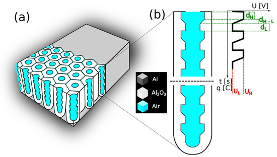
Figure 1.
A scheme of (a) the PAA-based DBR; and (b) the pore architecture with dH and dL segment thickness resulting from the anodization under UH and UL pulses, respectively (dH–L is the transition layer formed during the gradual voltage decrease from UH to UL).
In the pulse anodization two modes were applied: time- and charge-controlled mode. In the first mode the duration of UH = 50 V and UL = 20 V pulses was fixed to T = tH + tL = 660 s (where tH = 180, 140, 100, 60 s and tL = 480, 520, 560, 600 s), whereas the charge passing under each and subsequent UH and UL pulse was allowed to vary. In the second mode the charge density under each and subsequent UH and UL pulse was fixed (CH = 5017, 3661, 2598, 1535 mC/cm2 and CL = 2989, 3309, 3469, 3653 mC/cm2) and the duration of the UH and UL pulses (tH and tL, respectively) was allowed to vary. When the pulse anodization was accomplished, the remaining aluminum substrate was selectively detached from the PAA-based DBRs using a saturated solution of HCl/CuCl2. To avoid contact of PAA with the acid solution, the Al foil was removed only partially in the area limited by O-ring (Figure 2).
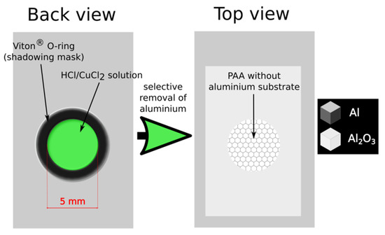
Figure 2.
A scheme representing the preparation of a free-standing porous anodic alumina (PAA).
The PAA-based photonic structures were studied by a field-emission scanning electron microscope FE-SEM (AMETEK, Inc., Mahwah, NJ, USA). The layer thickness of a given PAA sample was measured three times at different areas in the secondary electrons (SE) image and an average of the three measurements was used to calculate the dL (the layers formed under UL pulses) and the dH (the layers formed under UH pulses) thickness. The simulation of optical spectra was performed using the EPITAXYproject® epitaxy supporting software [28].
The transmission spectra were measured using the Fourier-transform infrared (FTIR) spectrometer Alpha II from Bruker Corp., Billerica, MA, USA. Each sample was measured in three spots through 2 mm diameter diaphragm. The spectra (16 scans per spectrum) were recorded in the range 1.66–25 um with spectral resolution of 2 cm−1
3. Results and Discussion
In our previous works [25,29], free-standing DBR structures were prepared by immersion entire samples in the CuCl2/HCl solution to remove remaining Al foil after the electrochemical process. This method most possibly resulted in upper layers’ delamination and exfoliation. Moreover, during the time the samples were immersed in the solution pores were subjected to an uncontrolled broadening due to the contact with the acid solution. Therefore, to circumvent these problems and to take a full control over the pore structure of the PAA-based DBRs after the synthesis, in this work the underlying Al substrate was removed only locally, while the other side of the sample (PAA) was protected by O-ring and had no contact with the CuCl2/HCl solution. Figure 2 shows a scheme of the procedure to prepare the samples and a free-standing DBR supported by the Al frame that was used to further analysis.
Anodizing parameters to synthesize the DBR structures were selected so that the spectral position of the first order PSB band (λ1) was in the 3500–5500 nm range (between the peak related with adsorbed water and the absorption bands associated with Al-O bond vibrations [29]). The following parameters were applied to fulfil this condition: UH = 50, UL = 20 V, UH- > UL rate = 0.234 V/s, 20 cycles and T = tH + tL = 660 s (the samples PAA tL–tH). At first, the influence of the immersion time in the CuCl2/HCl solution (tp) on optical properties of the PAA- based DBR structures was studied. To perform this analysis, this time a front side of the free-standing DBRs (top view in the Figure 2) was exposed to the contact with the solution, allowing the acid to penetrate to the open pores and react with Al2O3. In Figure 3, the transmittance (T) spectra of the PAA_600-60 sample are shown for different tp. The vertical, red, dotted line in all transmittance spectra denotes the OH group vibrations coming from adsorbed water [25,29]. As can be seen, the λ1 shifts towards blue part of the spectrum as the immersion time of the PAA_600-60 increases. At the same time, the peaks become more intensive and symmetrical (Figure 3). It is well known that the intensity of resonant peaks is optimized by increasing both the number of periods and the refractive index contrast between the low and high refractive index segments (∆n) [30,31,32,33]. Since in this case the number of pairs is constant (20-cycle processes), it can be concluded that lower transmittance is caused by the enhancement of the latter parameter. The ∆n, in turn, is induced by the tp, which via pore widening increases the layer porosity contrast. Owing to the obvious improvement of the optical characteristics (distinct and regular resonance peaks) with tp, the samples were immersed in the acid solution for 60 min before an optical comparison of the PAA-based DBRs anodized under time- and charge density-controlled modes.
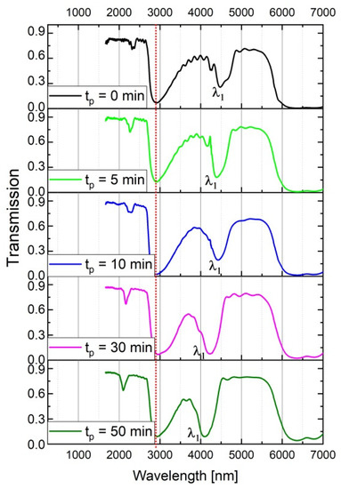
Figure 3.
Transmission spectra of the PAA_600-60 DBR for different tp.
Four PAA-based DBRs were produced under the time-controlled mode, where the duration of UH and UL pulses was varying while maintaining the tH + tL = 660 s. In Figure 4, the U(t) and ia(t) curves for the first three cycles and the corresponding transmission spectra of the PAAtL–tH samples (after tp = 60 min) are shown. First of all, it can be noted that the λ1 peaks in the MIR spectral range (>3000 nm) are very symmetrical and intensive (transmittance at the center of the λ1 is close to zero). Moreover, a simultaneous increase of the tL and decrease of the tH by 40 s makes the λ1 band to shift from ca. 5000 nm to 4000 nm.
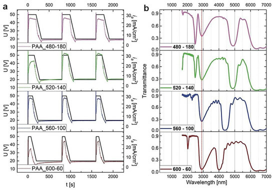
Figure 4.
(a) The U(t) (black solid lines) ia(t) (dotted lines) curves recorded during pulse anodization at 30 °C with various tH and tL (the samples PAA_ tL-tH) and other parameters as follows: UH = 50 V, UL = 20 V, UH->UL drop rate = 0.234 V/s, 20 cycles; (b) the corresponding transmission spectra recorded for the samples, after tp = 60 min.
It was demonstrated before that the time-controlled mode leads to a continuous reduction of the total amount of charge taking part in the anodization reaction that occurs under each UH and UL pulse [25,29]. As an effect, the dH and dL layers formed under the UH and UL pulses, respectively, become thinner with the anodization cycles. To avoid this problem, a program was written to control the total amount of charge passing under each UH and UL pulse (CH and CL, respectively) and the duration of the subsequent UH and UL pulses was regulated so that the same CH and CL was reached in every cycle (charge density-controlled mode). To compare the effect of changing the pulse anodization from time- to charge density-controlled mode, the CH and CL was determined from the ia(t) curves recorded for the PAA_tL–tH samples (Figure 4). Owing to the diffusion-limited processes which cause the increasing problem with the irregular development of dH + dL pairs, only the first three cycles were taken into account. Then, the mean of the three CH and CL values was calculated and used to design the pulse sequence under the charge density-controlled mode.
In Figure 5, the U(t) and ia(t) curves for the first three cycles recorded during pulse anodization under the charge density-controlled mode and the corresponding transmission spectra of the PAA_CL-CH samples (after tp = 60 min) are shown. It can be seen that upon switching the modes the λ1 peaks in the MIR spectral range became broader and asymmetric (blue edge of the peaks is split). Furthermore, the center position of the λ1 bands are red-shifted with respect to the corresponding peaks recorded for the PAA_tL–tH samples. In the transmittance spectrum of the sample PAA_2989-5017 the λ1 peak is presumably shifted above 6000 nm and thus is not visible, whereas the peak at around 3500 nm is the second order the PSB (λ2).
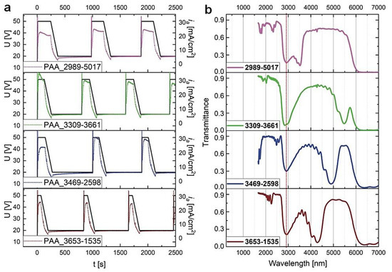
Figure 5.
(a) The U(t) (black solid lines) ia(t) (dotted lines) curves recorded during pulse anodization at 30 °C with various CH and CL in [mC/cm2] (the samples PAA_ CL-CH) and other parameters as follows: UH = 50 V, UL = 20 V, UH->UL drop rate = 0.234 V/s, 20 cycles; (b) the corresponding transmission spectra recorded for the samples after tp = 60 min.
In Figure 6, CH (the charge density for each UH pulse in the 20-cycle process) as a function of the number of cycles for both modes are demonstrated. It is seen that whereas CH decreases with increasing the number of cycles in the time-controlled mode, it is perfectly stable in the charge density-controlled mode. Since the thicknesses of anodized layers is determined by the amount of charge generated under a given anodization potential, this analysis strongly indicates that the dH + dL pairs grow uniformly in the PAA_CL-CH samples, in contrast to the pairs formed in the PAA_tL-tH samples.
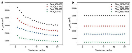
Figure 6.
CH as a function of the number of cycles determined for (a) time- and (b) charge density-controlled mode pulse anodization.
In Figure 7, SEM images of the upper dH and dL pairs (the layers grown in the last 16–20 cycles) from the PAA_tL-tH samples are juxtaposed with the images of the corresponding dH and dL pairs from the PAA_CL-CH samples. The morphological analysis shows that the upper dH and dL layers in the PAA_CL-CH samples are thicker than the ones in the corresponding PAA_tL-tH samples, which is in agreement with the higher CH values (and CL values—not shown in Figure 7) that were reached in the last anodizing cycles performed under the charge-controlled mode (Figure 7).
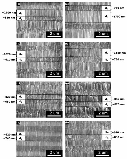
Figure 7.
SEM images of upper dH and dL segments in the PAA_tL-tH DBRs: (a) PAA_480-180, (b) PAA_520-140, (c) PAA_560-100, (d) PAA_600-60; and in the PAA_CL-CH DBRs: (e) PAA_2989-5017, (f) PAA_3309-3661, (g) PAA_3469-2598, (h) PAA_3653-1535.
For better visualization, the first order PSBs generated by the DBRs prepared in time- and charge density-controlled modes are shown in a narrower spectral range (Figure 8). In Table 1, transmittance at λ1 central position (T0) and the full width-half maximum (FWHM) of the λ1 peak determined for the PAA_tL-tH and PAA_CL-CH DBRs are gathered (except the PAA_2989-5017 sample, for which the λ1 peak was out of the detection range). The FWHM of the first order PSB was determined from the experimental transmittance curves at T = (Tmax − T0)/2 (Figure 8). In the calculation, Tmax was taken as the highest value of T in the range of 3500–5500 nm. Despite some uncertainty in determination of the FWHM for the PAA_CL-CH DBRs caused by the wavy blue side of the λ1 peaks, it can be seen that the FWHM is comparable for the DBRs fabricated by the time-controlled mode (a slight decrease in FWHM can be noticed for the PAA_600-60 sample) and it tends to increase in the corresponding DBRs produced by the charge density-controlled mode.
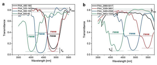
Figure 8.
The λ1 peaks in the PAA-based DBRs anodized under (a) time-controlled mode and (b) charge density-controlled mode.

Table 1.
Transmittance at λ1 central position (T0) and the full width-half maximum (FWHM) of the λ1 peak determined for the PAA_tL-tH and PAA_CL-CH DBRs.
The bandwidth of the PSB depends mainly on the ∆n: the larger the refractive index contrast, the larger the FWHM [34,35]. The ∆n in PAA-based DBR is determined by the contrast in porosity of the dH and dL layers. The porosity, in turn, depends fully on the anodization parameters such as the applied anodizing voltage and temperature, which define both the interpore distance (Dc) and the pore diameter (Dp). Since the PAA-based DBRs were all produced under the same pulse sequence (UH = 50 V, UL = 20 V) and anodizing temperature, the porosity of the dH and dL segments ( [25]) and thus the nH and nL (∆n = (nL2 − nH2)/2nL2 = constant) should not vary. In Table 2, the spectral position of the λ1 and λ2 bands extracted from the simulated spectra are gathered. The optical spectra were simulated taking into account the thickness of the upper dH and dL pairs (Figure 7) and assuming the same ∆n = 0.06 for all samples. As can be seen, both bands are in a good agreement with the observed ones (Figure 4b, Figure 5b and Figure 8). The simulation also confirms that the peak at around 3500 nm in the spectrum of the sample PAA_2989-5017 comes from the λ2. The small discrepancies between the observed and calculated λ1 and λ2 bands as well as the variable PSB broadening can result from the different pulses’ duration and thus the entire process. The longer anodization time will cause a larger pore broadening (larger Dp) and larger the dH and dL layers’ porosity and, as a consequence, the nH and nL will change. The ∆n can be also slightly affected by the Al2O3 refractive index variation itself with the wavelength (the n of Al2O3 is decreasing from 1.67 to 1.62 when the wavelength is increasing from 4 to 5 μm [36]). Owing to the same number of pairs in all studied multilayer stacks, the λ1 intensity (T0) are comparable in both type of samples. A minor difference in T0 is due to the probable slight variation of the ∆n in the real samples.
Table 2.
The spectral position of the λ1 and λ2 bands calculated using EPITAXYproject® software and assuming the same refractive indices (nH = 1.43 and nL = 1.52) for all samples.
Since the charge density-controlled mode apparently improves the uniformity of the grown porous layers, the question arises what the reason is for PSB peak asymmetry in the PAA_CL-CH samples. In the transmittance spectra Fabry-Pérot (F-P) interference fringes (low intensity oscillations of increasing spacing with the wavelength) are also visible. The F-P fringes originate from the interference of the beam reflected from the two interfaces between the top and the bottom part of PAA and air [37]. The F-P interference can superimpose the PSBs to some extend depending on the PAA thickness, its uniformity in the measurement area, PBS spectral position and intensity, etc. However, since only the blue edge of the λ1 peak in the PAA_CL-CH samples seems to be affected by this phenomenon, there can be also an alternative explanation for the peak asymmetry in these particular DBRs. As it is well established, the center position of photonic stop bands (PSBs) is governed by the Bragg-Snell law [38]. For the angle of incidence θ equal to 0, the law can be expressed as follows:
where λm is the wavelength of a photonic stop band (PSB), m is the order of the PSB, d is the periodicity (d = dH + dL) and neff is the effective refractive index (neff = (nHdH + nLdL)/(dH + dL)). Thus, for the larger d neff the PSBs will shift toward red part of the spectrum (Figure 9).
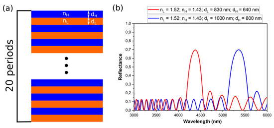
Figure 9.
A scheme of the PAA-based DBR (a); the reflectance spectra of two DBR structures with the same number of dH + dL pairs (20 periods), ∆n = 0.06 and different optical thickness d neff (b).
Since during pulse anodization the successive dH and dL layers may differ in both thickness and porosity, the right side of the Equation (1) is actually a compilation of different values of the d neff product and can be rewritten as follows:
where p is the number of dH + dL pairs in a DBR.
In the PAA based DBRs synthesized by the time-controlled mode both d and neff vary with subsequent layers grown upon the following anodization cycles. Owing to the diffusion-limited problems the d becomes successively smaller and therefore, the last layers are thinner than the first ones (d1 > d2 > … > d20). On the other hand, due to the extending time of anodization the layers produced at the beginning of the process are subjected to longer reaction with acidic electrolyte and thus pores in the first dH + dL pairs become wider than the ones in the last dH + dL pairs. Therefore, the neff of the last layers is larger than the neff of the first ones (n1eff < n2eff < …< n20eff). So the smaller d values of the dH + dL pairs produced at the end of the process are counterbalanced by their larger neff. As a consequence, the product dp∙npeff of each dH + dL pair is optically equalized giving symmetric and intensive PSBs. As pore are broadened after the synthesis, the compensation effect is even stronger leading to PSBs with almost zero transmittance. In the PAA based DBRs synthesized by the charge density-controlled mode the d is the same in every cycle (d1 = d2 = … = d20), whereas the neff remains progressively changing due to the different porosity of the dH + dL pairs, namely the n1eff < n2eff < …< n20eff. Therefore, the ∆neff is not counterbalanced by the ∆d resulting in variation of the product dp∙npeff within the multilayer stack. Consequently, the Bragg-Snell relation is fulfilled only for few dH + dL out of the total 20 pairs. The other pairs provide different optical conditions and accordingly the PSB is centered at slightly different spectral position for these specific pairs. As an effect, the resonance band in the MIR region split and broaden. In fact, owing to the inhomogeneous porosity that remained in the subsequent dH and dL layers of equal thickness, a few DBRs can be formed in one multilayer stack. If two DBRs are created, the Equation (2) is divided into two terms:
In addition:
where pI and pII (p = pI + pII) comprises the number of dH + dL pairs that makes up DBRI and DBRII, respectively. Each of DBRs are built of alternating double-layers characterized by similar optical thickness (d neff).
Furthermore, during the contact with the CuCl2/HCl solution after the electrochemical synthesis the upper layers are more exposed to the interaction with the acid than the lower ones (close to the barrier layer). As a consequence, the ∆neff increases. This effect holds for both PAA_tL-tH and PAA_ CL-CH samples. However, in the latter samples the increasing ∆neff is not counterbalanced by decreasing d values (∆d = 0), what should be reflected in a different optical behavior of the PAA_ CL-CH samples with increasing tp. To check this assumption, the influence of the tp on the optical spectra of the PAA_3653-1535 sample was studied (Figure 10). As expected, in contrast to the PSBs generated by the PAA_600-60 DBR (Figure 3), the λ1 peaks in the transmission spectra of the corresponding PAA_3653-1535 DBR become wider and more asymmetrical with tp. Upon prolonged contact with the CuCl2/HCl solution refractive index of each and subsequent layer become closer to that of air. Accordingly, the products dp∙npeff acquire smaller and the PSB shifts to shorter wavelengths as tp increases. In the case of the PAA_3653-1535 DBR, the λ1 band centered at the lowest T shifts from ca. 4900 nm to about 4600 nm when tp changes from 0 to 50 min. Moreover, the increasing tp enhances the n1eff < n2eff < … < n20eff inequality (n1eff << n20eff) making thereby the spacing between λmI and λmII larger (Figure 10).
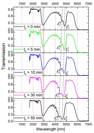
Figure 10.
Transmission spectra of the PAA_3653-1535 for different tp.
The optical properties of the PAA-based DBRs studied in this work could be attractive for application in transparent photonic crystal heat mirror (TPCHM) [39,40]. In principle, TPCHM works as infrared mirrors that decrease heat losses in the receiver of solar concentrators [36]. Precisely, TPCHM should selectively reflect the infrared spectral region while being transparent towards solar irradiance [35]. Such requirements could be fulfilled by the PAA-based DBR after a proper design of the pulse sequence. To make the DBRs more transparent in the 250–2500 nm region (to remove the higher order PSBs [26]) a pulse sequence with a gradual change of applied voltage/current density can be applied (e.g., Gaussian pulse profile) that will induce periodical and gradual refractive index change within the DBRs. The reflection in the MIR region can be enhanced by increasing the number of refractive layers in a DBR stack. The optimization of the material requires, however, further experimental studies supported by adequate theoretical modelling.
4. Conclusions
In this work PAA- based DBRs were synthesized by pulse anodization. Two modes were used to design the DBR structures: time- (the PAA_tL-tH DBRs) and charge density-controlled (PAA_CL-CH DBRs) mode. After the electrochemical synthesis the PAAs were immersed in a saturated CuCl2/HCl solution for a given time. The influence of the immersion time (tp) on optical characteristics of the samples was systematically studied. With increasing tp the photonic stopbands (PSBs) became more intensive and shifted towards blue part of the spectrum. In the PAA_tL-tH DBRs, dH + dL pairs of variable thickness (∆d) under each and successive UH and UL pulse were grown. It was suggested that in this type of samples the ∆d was counterbalanced by variable porosity of respective segments (translating into variable effective refractive index, ∆neff) leading to symmetric PSBs. The pore broadening in the acid solution strengthened the compensation effect. As a consequence, the first order PSBs became more symmetrical and intensive (transmission ~0) with increasing tp. The application of the charge density-controlled mode resulted in an uniform formation of dH and dL layers (∆d = 0) under each and successive UH and UL pulses, respectively. Owing to the equalized thickness of the dH + dL pairs, the ∆neff was not counterbalance by ∆d. As a result, the λ1 bands were wider, split on the blue edge side and red-shifted with reference to those of corresponding PAA tL-tH DBRs. Pore widening after the electrochemical synthesis only enhanced this trend: the PSBs became more broadened and split on their blue edge in the PAA_CL-CH DBRs as the immersion time (td) increased.
Author Contributions
Conceptualization, M.N.; electrochemical synthesis of PAA-based PCs and data analysis, E.B. and G.S.; optical measurements, M.K. and E.B.; SEM analysis, M.N.; writing—original draft preparation, M.N.; writing—review and editing, G.S.; visualization, M.N. and G.S. All authors have read and agreed to the published version of the manuscript.
Funding
The research was financed by the National Science Centre, Poland (UMO-2019/35/B/ST5/01025). The work was co-financed by Military University of Technology under research project UGB 22-845/2021/WAT. The UV-vis-NIR spectrometers used in these studies were obtained with funds from the Polish Ministry of Science and Higher Education grant for investment in large research infrastructure no. 7044/IA/SP/2019.
Conflicts of Interest
The authors declare no conflict of interest.
References
- Krauss, T.F.; De La Rue, R.M. Photonic crystals in the optical regime—Past, present and future. Prog. Quantum Electron. 1999, 23, 51–96. [Google Scholar] [CrossRef]
- Wang, B.; Fei, G.T.; Wang, M.; Kong, M.G.; Zhang, L. De Preparation of photonic crystals made of air pores in anodic alumina. Nanotechnology 2007, 18, 365601. [Google Scholar] [CrossRef]
- Pavesi, L. Porous silicon dielectric multilayers and microcavities. Riv. Nuovo Cimento 1997, 20, 1–76. [Google Scholar] [CrossRef]
- Masuda, H.; Fukuda, K. Ordered Metal Nanohole Arrays Made by a Two-Step Replication of Honeycomb Structures of Anodic Alumina. Science 1995, 268, 1466–1468. [Google Scholar] [CrossRef] [PubMed]
- Law, C.S.; Lim, S.Y.; Abell, A.D.; Voelcker, N.H.; Santos, A. Nanoporous anodic alumina photonic crystals for optical chemo-and biosensing: Fundamentals, advances, and perspectives. Nanomaterials 2018, 8, 788. [Google Scholar] [CrossRef] [PubMed]
- Law, C.S.; Lim, S.Y.; Santos, A. On the Precise Tuning of Optical Filtering Features in Nanoporous Anodic Alumina Distributed Bragg Reflectors. Sci. Rep. 2018, 8, 1–16. [Google Scholar] [CrossRef] [PubMed]
- Chen, Y.; Santos, A.; Wang, Y.; Kumeria, T.; Ho, D.; Li, J.; Wang, C.; Losic, D. Rational Design of Photonic Dust from Nanoporous Anodic Alumina Films: A Versatile Photonic Nanotool for Visual Sensing. Sci. Rep. 2015, 5, 12893. [Google Scholar] [CrossRef]
- Zhao, H.; Liu, L.; Lei, Y. A mini review: Functional nanostructuring with perfectly-ordered anodic aluminum oxide template for energy conversion and storage. Front. Chem. Sci. Eng. 2018, 12, 481–493. [Google Scholar] [CrossRef]
- Ruiz-Clavijo, A.; Caballero-Calero, O.; Martín-González, M.S. Revisiting anodic alumina templates: From fabrication to applications. Nanoscale 2021, 13, 2227–2265. [Google Scholar] [CrossRef]
- Kumeria, T.; Rahman, M.M.; Santos, A.; Ferré-Borrull, J.; Marsal, L.F.; Losic, D. Nanoporous Anodic Alumina Rugate Filters for Sensing of Ionic Mercury: Toward Environmental Point-of-Analysis Systems. ACS Appl. Mater. Interfaces 2014, 6, 12971–12978. [Google Scholar] [CrossRef]
- Ferré-Borrull, J.; Pallarès, J.; Macías, G.; Marsal, L.F. Nanostructural Engineering of Nanoporous Anodic Alumina for Biosensing Applications. Materials 2014, 7, 5225–5253. [Google Scholar] [CrossRef] [PubMed]
- Gorelik, V.S.; Klimonsky, S.O.; Filatov, V.; Napolskii, K.S. Optical properties of one-dimensional photonic crystals based on porous films of anodic aluminum oxide. Opt. Spectrosc. 2016, 120, 534–539. [Google Scholar] [CrossRef]
- Kumeria, T.; Santos, A.; Rahman, M.M.; Ferré-Borrull, J.; Marsal, L.F.; Losic, D. Advanced Structural Engineering of Nanoporous Photonic Structures: Tailoring Nanopore Architecture to Enhance Sensing Properties. ACS Photon. 2014, 1, 1298–1306. [Google Scholar] [CrossRef]
- Lee, W.; Ji, R.; Gösele, U.; Nielsch, K. Fast fabrication of long-range ordered porous alumina membranes by hard anodization. Nat. Mater. 2006, 5, 741–747. [Google Scholar] [CrossRef]
- Lee, W.; Park, S.-J. Porous anodic alumina oxide: Anodization and templated synthesis of functional nanostructures. Chem. Rev. 2014, 114, 7487–7556. [Google Scholar] [CrossRef]
- Santos, A.; Yoo, J.H.; Rohatgi, C.V.; Kumeria, T.; Wang, Y.; Losic, D. Realisation and advanced engineering of true optical rugate filters based on nanoporous anodic alumina by sinusoidal pulse anodisation. Nanoscale 2015, 8, 1360–1373. [Google Scholar] [CrossRef]
- Law, C.S.; Santos, A.; Nemati, M.; Losic, D. Structural Engineering of Nanoporous Anodic Alumina Photonic Crystals by Sawtooth-like Pulse Anodization. ACS Appl. Mater. Interfaces 2016, 8, 13542–13554. [Google Scholar] [CrossRef]
- Acosta, L.K.; Berto-Rosello, F.; Xifre-Perez, E.; Law, C.S.; Santos, A.; Ferré-Borrull, J.; Marsal, L.F. Tunable Nanoporous Anodic Alumina Photonic Crystals by Gaussian Pulse Anodization. ACS Appl. Mater. Interfaces 2020, 12, 19778–19787. [Google Scholar] [CrossRef] [PubMed]
- Santos, A. Nanoporous anodic alumina photonic crystals: Fundamentals, developments and perspectives. J. Mater. Chem. C 2017, 5, 5581–5599. [Google Scholar] [CrossRef]
- Baghdasaryan, T.; Geernaert, T.; Chah, K.; Caucheteur, C.; Schuster, K.; Kobelke, J.; Thienpont, H.; Berghmans, F. Anomalous transparency in photonic crystals and its application to point-by-point grating inscription in photonic crystal fibers. Sci. Rep. 2018, 8, 5470. [Google Scholar] [CrossRef]
- Starkey, T.; Vukusic, P. Light manipulation principles in biological photonic systems. Nanophotonics 2013, 2, 289–307. [Google Scholar] [CrossRef]
- Rahman, M.M.; Garcia-Caurel, E.; Santos, A.; Marsal, L.F.; Pallarès, J.; Ferré-Borrull, J. Effect of the anodization voltage on the pore-widening rate of nanoporous anodic alumina. Nanoscale Res. Lett. 2012, 7, 474. [Google Scholar] [CrossRef]
- Wang, D.; Zhang, L.; Lee, W.; Knez, M.; Liu, L. Novel Three-Dimensional Nanoporous Alumina as a Template for Hierarchical TiO2Nanotube Arrays. Small 2012, 9, 1025–1029. [Google Scholar] [CrossRef]
- Hierro-Rodriguez, A.; Rocha-Rodrigues, P.; Valdés-Bango, F.; Alameda, J.M.; Jorge, P.A.S.; Santos, J.L.; de Araújo, J.P.E.; Teixeira, J.; Guerreiro, A. On the anodic aluminium oxide refractive index of nanoporous templates. J. Phys. D Appl. Phys. 2015, 48, 455105. [Google Scholar] [CrossRef]
- Białek, E.; Włodarski, M.; Norek, M. Fabrication of Porous Anodic Alumina (PAA) by High-Temperature Pulse-Anodization: Tuning the Optical Characteristics of PAA-Based DBR in the NIR-MIR Region. Materials 2020, 13, 5622. [Google Scholar] [CrossRef]
- Becker, M.; Vant-Hull, L.L. Thermal Receivers. In Solar Power Plants, 1st ed.; Winter, C.-J., Sizmann, R.L., Vant-Hull, L.L., Eds.; Springer—Verlag: Berlin, Germany, 1991; pp. 163–198. [Google Scholar]
- Estrada-Wiese, D.; Del Rio, J.A.; De La Mora, M.B. Heat transfer in photonic mirrors. J. Mater. Sci. Mater. Electron. 2014, 25, 4348–4355. [Google Scholar] [CrossRef][Green Version]
- EPITAXYproject®. Available online: http://www.epitaxyproject.com/ (accessed on 31 July 2021).
- Białek, E.; Włodarski, M.; Norek, M. Influence of Anodization Temperature on Geometrical and Optical Properties of Porous Anodic Alumina(PAA)-Based Photonic Structures. Materials 2020, 13, 3185. [Google Scholar] [CrossRef] [PubMed]
- Admassu, D.; Durowade, T.; Sellers, R.; Sivananthan, S. Effect of interface grading on the optical performance of distributed Bragg reflector multilayers in Fabry-Pérot optical filters. Microsyst. Technol. 2020, 27, 2785–2790. [Google Scholar] [CrossRef]
- Lee, G.; Scripka, D.A.; Wagner, B.; Thadhani, N.N.; Kang, Z.; Summers, C.J. Design and fabrication of distributed Bragg reflector multilayers for dynamic pressure sensing. Opt. Expr. 2017, 25, 27067–27076. [Google Scholar] [CrossRef] [PubMed]
- Mrázek, J.; Spanhel, L.; Matějec, V.; Bartoň, I.; Džunda, R.; Puchý, V. Nanocrystalline Zn2TiO4 films for distributed Bragg's reflectors operating in near infrared region. Opt. Mater. 2021, 112, 110805. [Google Scholar] [CrossRef]
- Gao, B.; George, J.P.; Beeckman, J.; Neyts, K. Design, fabrciation and characterization of a distributed Bragg reflector for reducing the étendue of a wavelenght converting system. Opt. Expr. 2020, 28, 12837–12846. [Google Scholar] [CrossRef]
- Paternò, G.M.; Manfredi, G.; Scotognella, F.; Lanzani, G. Distributed Bragg reflectors for the colorimetric detection of bacterial contaminants and pollutants for food quality control. APL Photon. 2020, 5, 080901. [Google Scholar] [CrossRef]
- Yaun, Z.-S.; Jhang, J.-M.; Yu, P.-H.; Jiang, C.-M.; Huang, Y.-C.; Wu, Y.-L.; Lin, J.-J.; Yang, C.-F. Comparisons of theoretical and exeprimantal results of blue light SiO2-Nb2O5 distributed Bragg reflector fabricated using e-beam deposition. Vacuum 2020, 182, 109782. [Google Scholar] [CrossRef]
- RefractiveIndex.INFO. Available online: https://refractiveindex.info/?shelf=main&book=Al2O3&page=Malitson-o (accessed on 31 July 2021).
- Kushnir, S.E.; Napolskii, K.S. Thickness-dependent iridescence of one-diensional photonic crystals based on anodic alumina. Mater. Des. 2018, 144, 140–150. [Google Scholar] [CrossRef]
- Ozin, G.A.; Arsenault, A. Nanochemistry: A chemical Approach to Nanomaterials, 2nd ed.; Royal Society of Chemistry: London, UK, 2015. [Google Scholar]
- Rostami, M.; Talebzadeh, N.; O’Brien, P.G. Transparent Photonic Crystal Heat Mirrors for Solar Thermal Applications. Energies 2020, 13, 1464. [Google Scholar] [CrossRef]
- Rostami, M.; Pirvaram, A.; Talebzadeh, N.; O’Brien, P.G. Numerical evaluation of one-dimensional transparent photonic crystal heat mirror coatings for parabolic dish concentrator receivers. Renew. Energy 2021, 171, 1202–1212. [Google Scholar] [CrossRef]


Publisher’s Note: MDPI stays neutral with regard to jurisdictional claims in published maps and institutional affiliations. |
© 2021 by the authors. Licensee MDPI, Basel, Switzerland. This article is an open access article distributed under the terms and conditions of the Creative Commons Attribution (CC BY) license (https://creativecommons.org/licenses/by/4.0/).