
A Novel Single-Inductor Bipolar-Output DC/DC Boost Converter for OLED Microdisplays

 ,
,  , , ,
, , ,  ,
,  , , and
Abstract
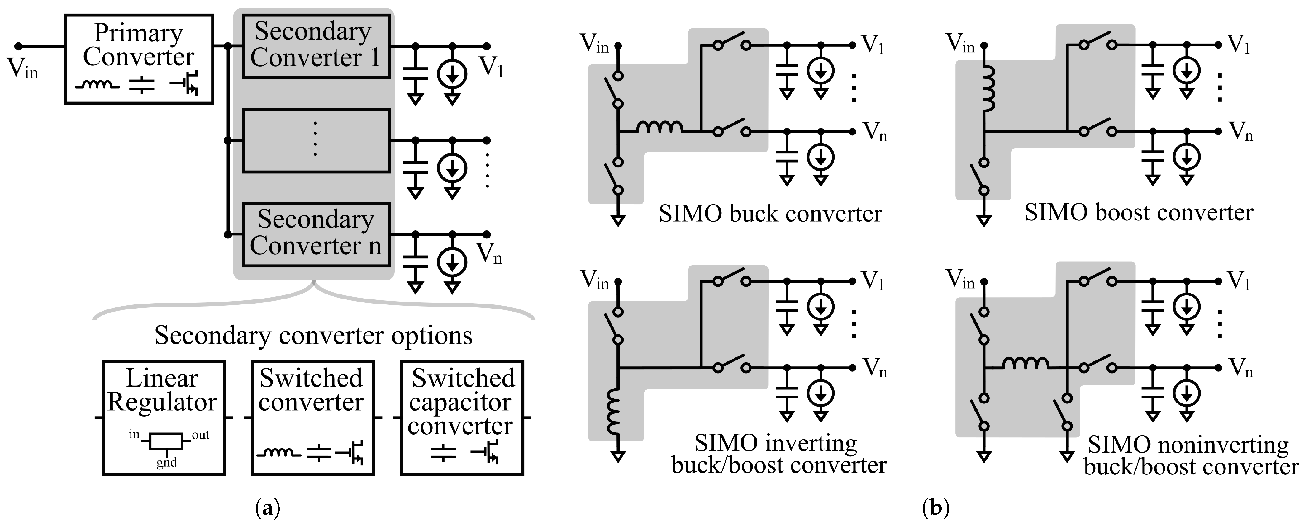
:1. Introduction
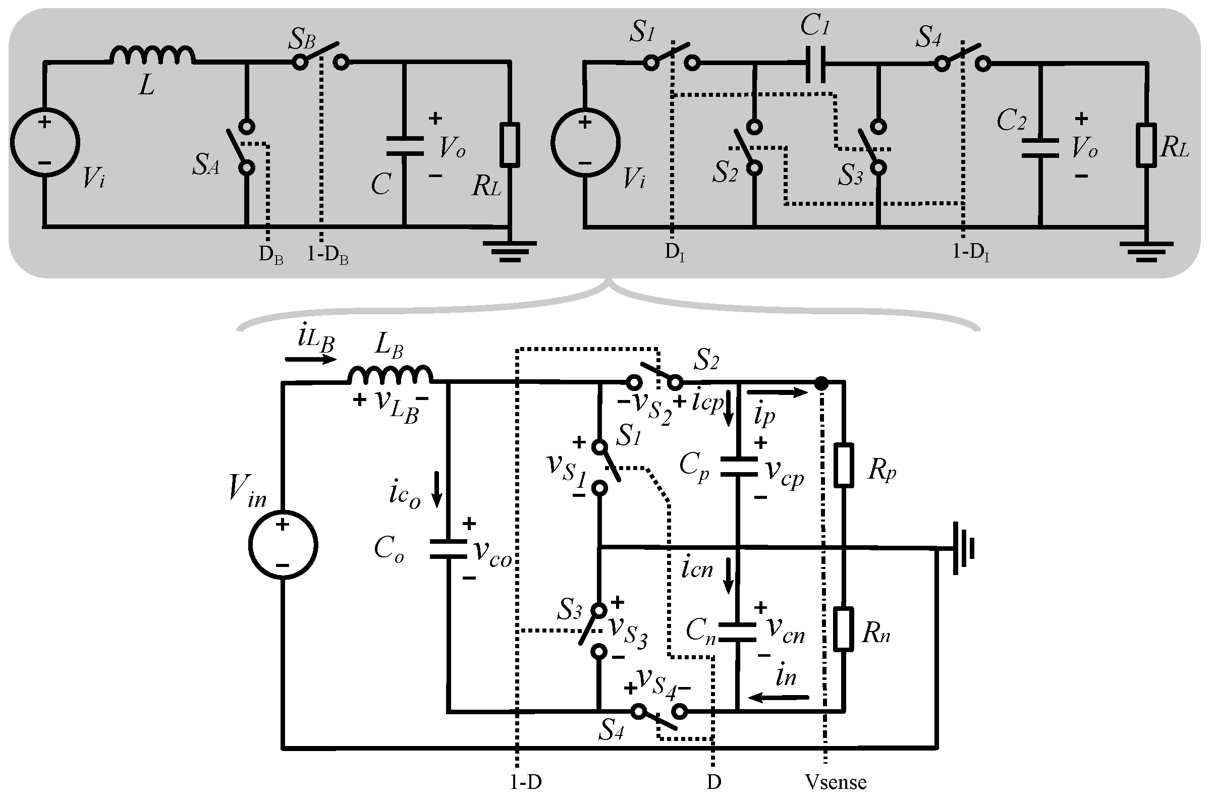
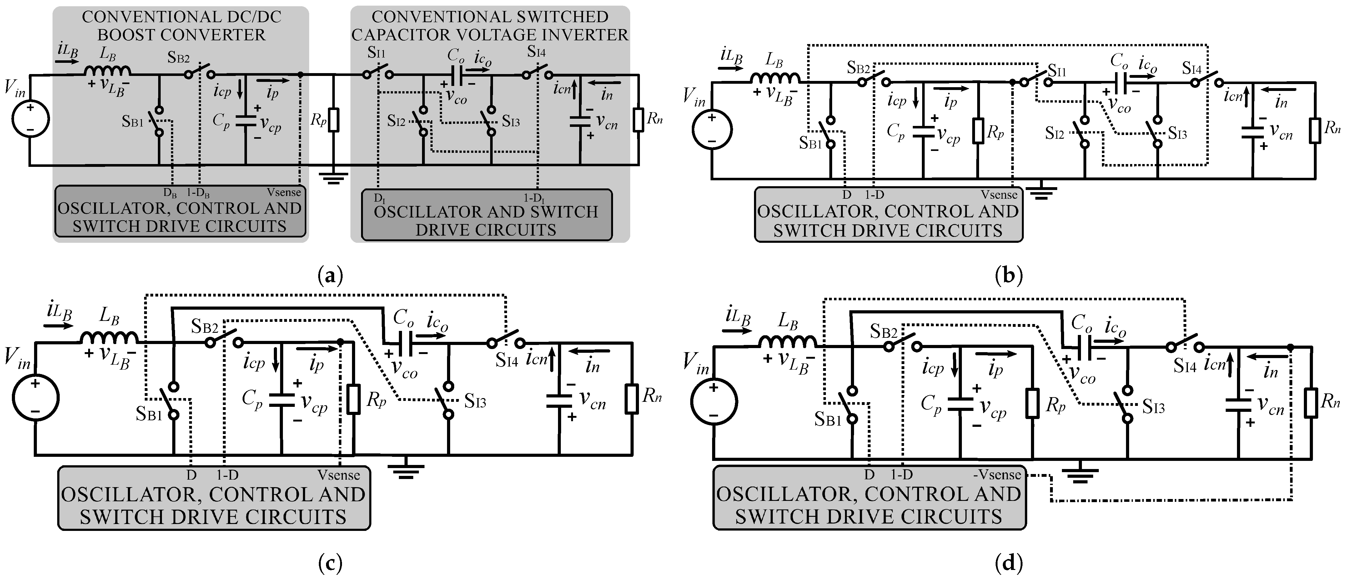
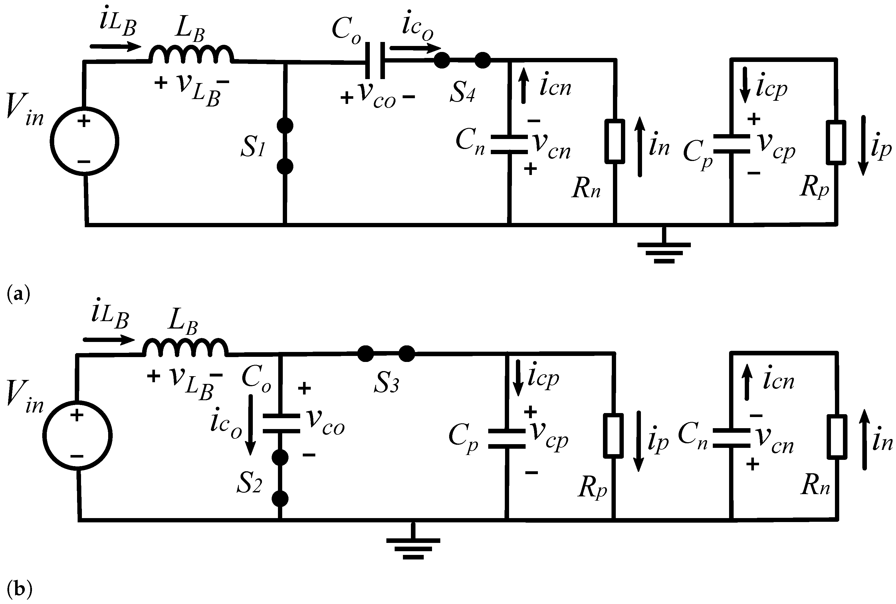
2. Topology Derivation
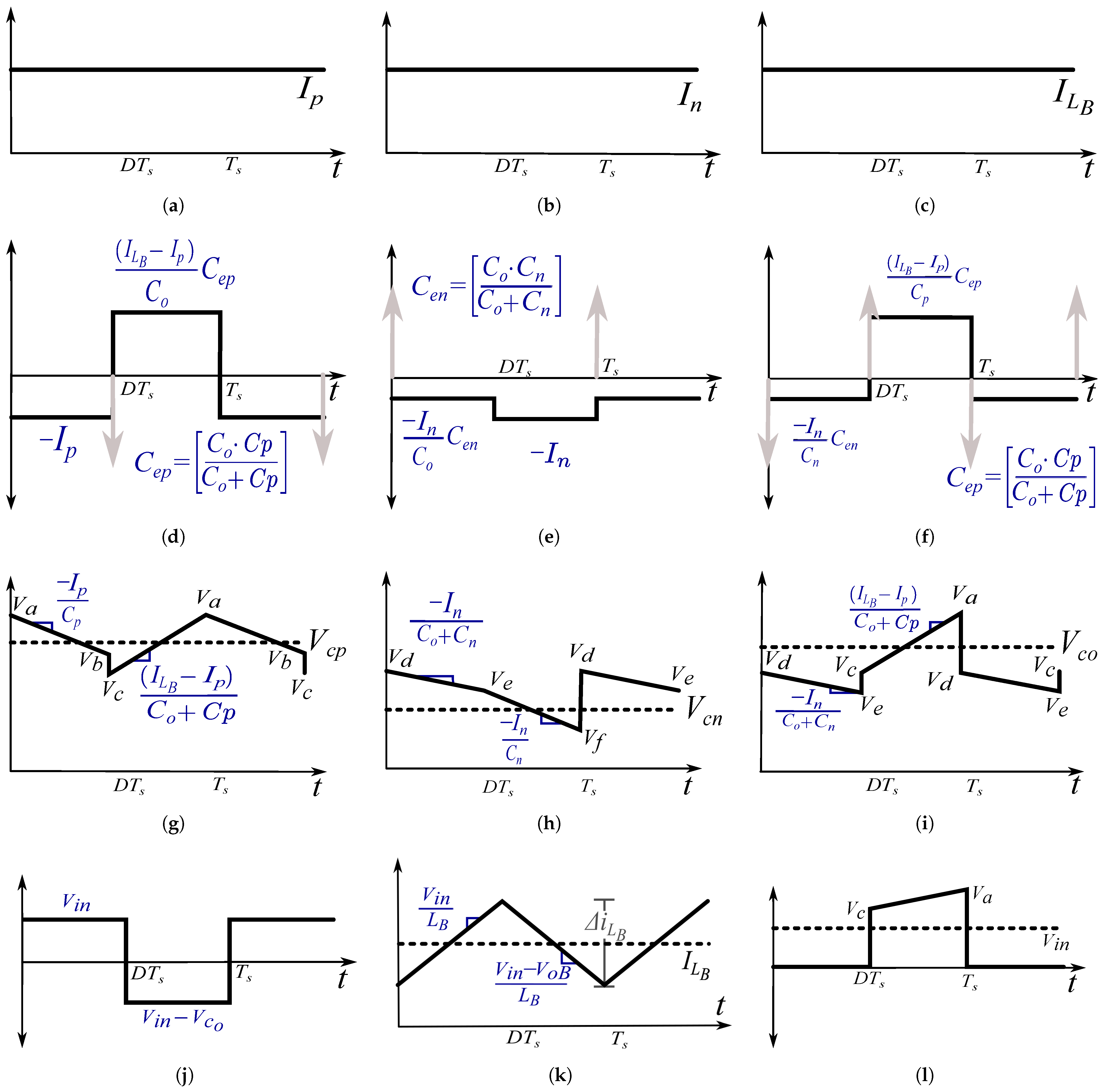
3. CCM Operation of the Proposed Topology
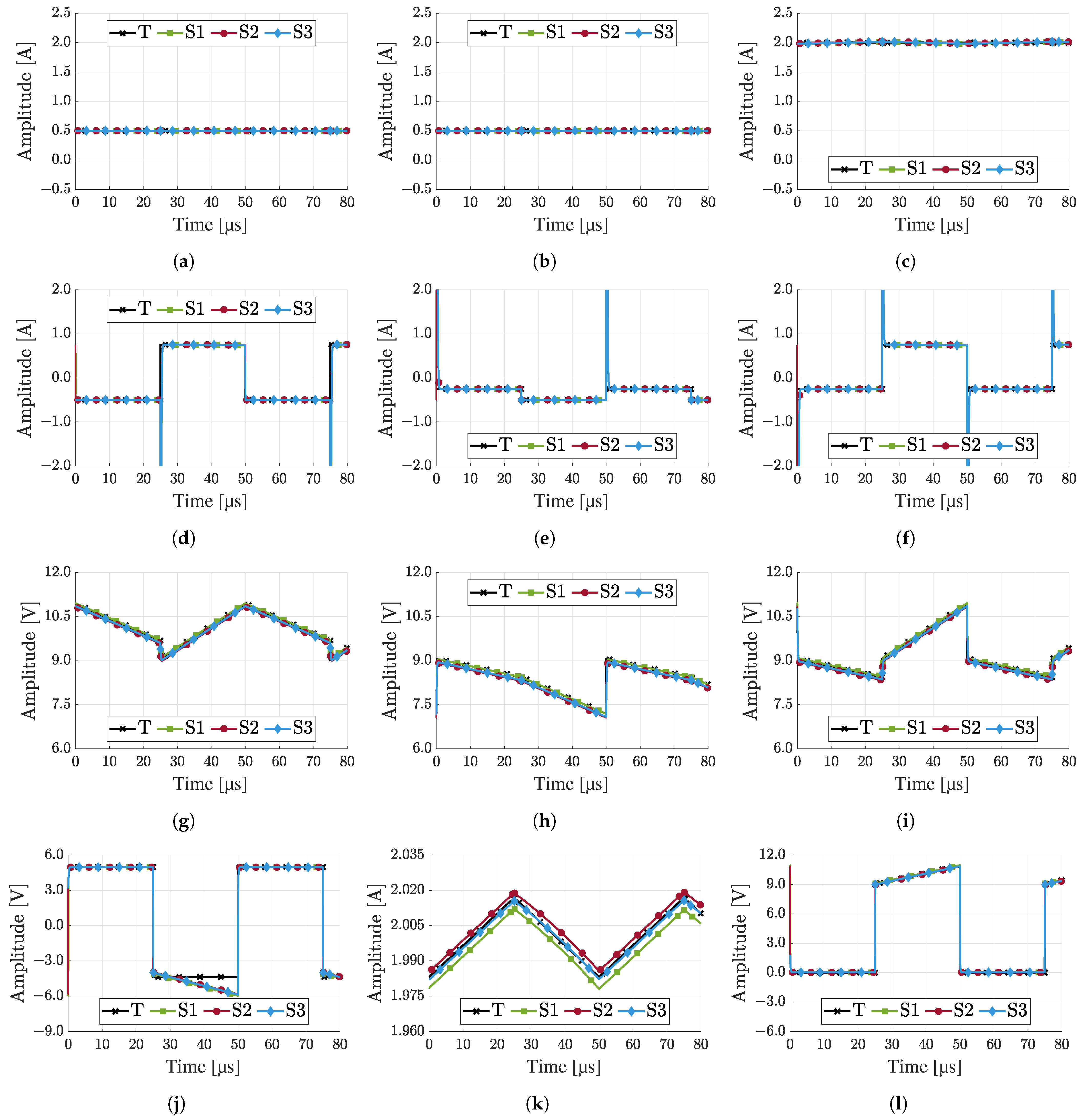
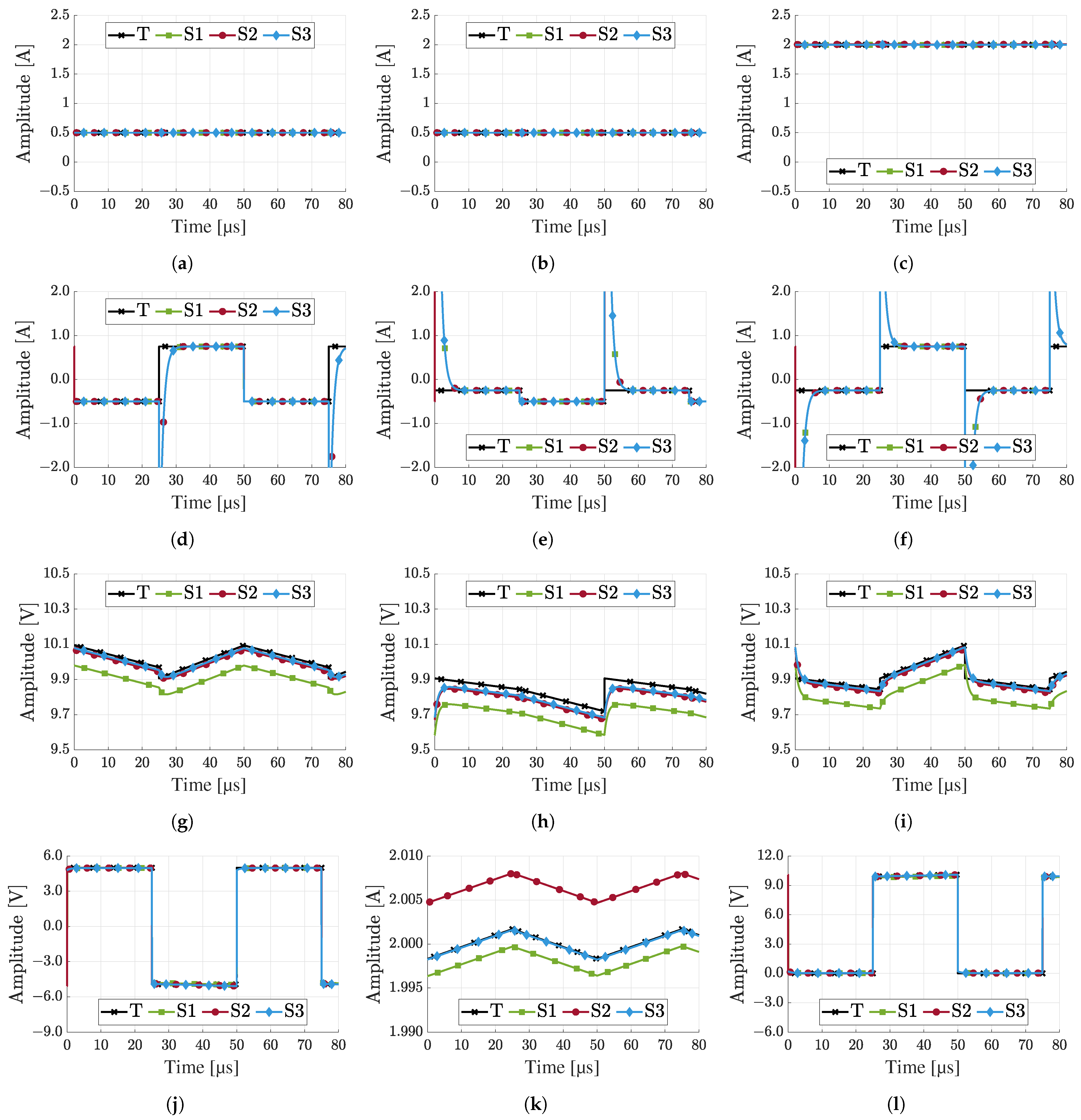
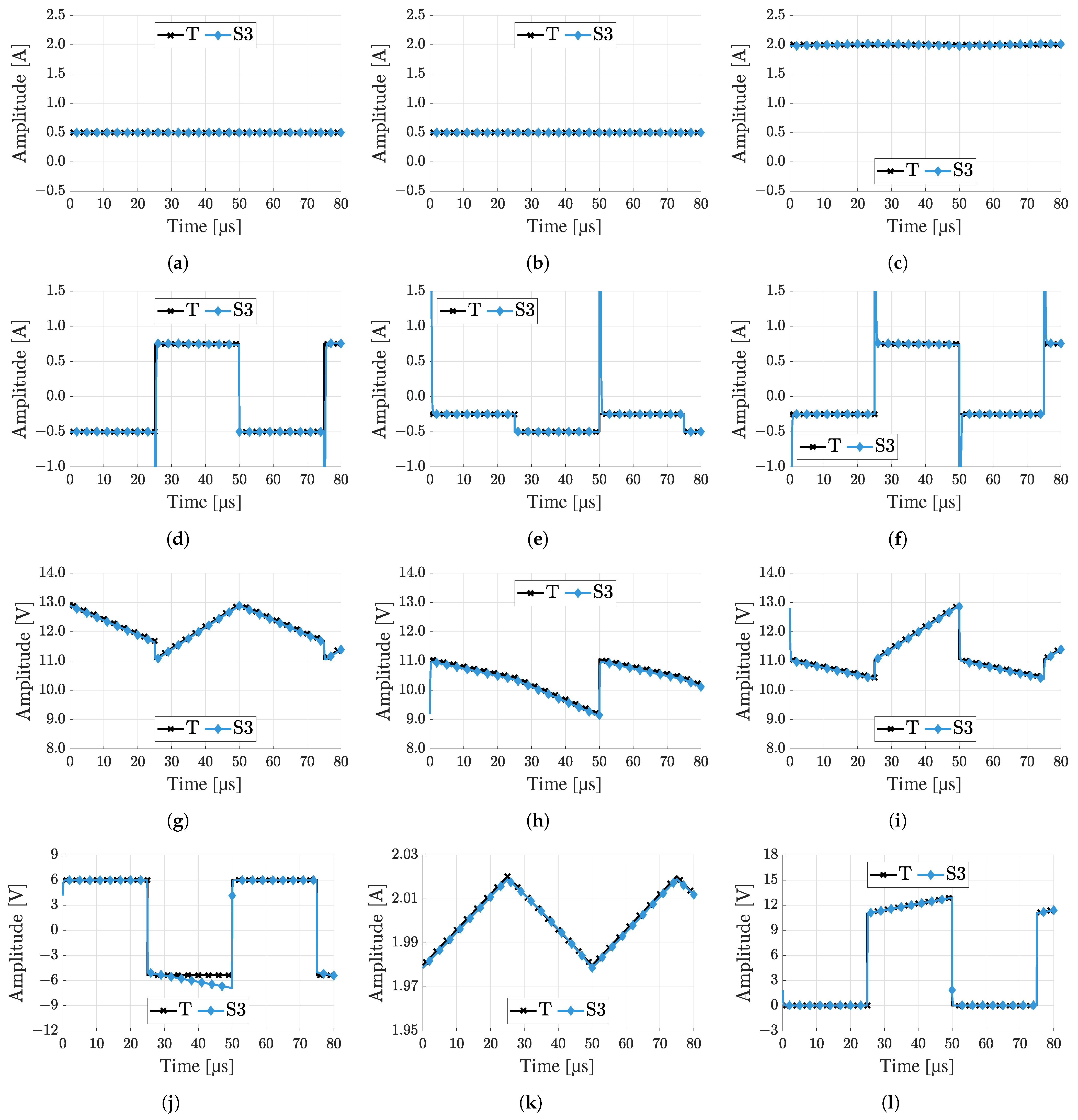
4. Evaluation of the Converter
5. Conclusions
Author Contributions
Funding
Institutional Review Board Statement
Informed Consent Statement
Data Availability Statement
Acknowledgments
Conflicts of Interest
Abbreviations
| SIBO | Single-Inductor Bipolar-Output |
| DC | Direct Current |
| SISO | Single-Inductor Single-Output |
| SIMO | Single-Inductor Multiple-Output |
| CCM | Continuous Conduction Mode |
| DCM | Discontinuous Conduction Mode |
| MAPE | Mean Absolute Percentage Error |
| SD | Standard Deviation |
References
- Chen, H.W.; Lee, J.H.; Lin, B.Y.; Chen, S.; Wu, S.T. Liquid crystal display and organic light-emitting diode display: Present status and future perspectives. Light. Sci. Appl. 2018, 7, 17168. [Google Scholar] [CrossRef] [PubMed]
- Vaidya, V.; Soggs, S.; Kim, J.; Haldi, A.; Haddock, J.N.; Kippelen, B.; Wilson, D.M. Comparison of Pentacene and Amorphous Silicon AMOLED Display Driver Circuits. IEEE Trans. Circuits Syst. I Regul. Pap. 2008, 55, 1177–1184. [Google Scholar] [CrossRef]
- Dyson, M.J. 57-1: Trends in Low-Cost Displays for Emerging Applications; SID Symposium Digest of Technical Papers; Wiley Online Library: Hoboken, NJ, USA, 2021; Volume 52, pp. 799–801. [Google Scholar]
- Huang, Y.; Hsiang, E.L.; Deng, M.Y.; Wu, S.T. Mini-LED, Micro-LED and OLED displays: Present status and future perspectives. Light. Sci. Appl. 2020, 9, 1–16. [Google Scholar] [CrossRef] [PubMed]
- Virey, E.H.; Baron, N.; Bouhamri, Z. 30-4: MicroLED Display Technology Trends and Intellectual Property Landscape; SID Symposium Digest of Technical Papers; Wiley Online Library: Hoboken, NJ, USA, 2020; Volume 51, pp. 436–439. [Google Scholar]
- Lin, Z.R.; Chiu, H.J. Design and Implementation of Solar OLED Lighting Driver Circuit with Frequency Modulation Control. Energies 2020, 13, 5608. [Google Scholar] [CrossRef]
- Mao, F.; Lu, Y.; Bonizzoni, E.; Boera, F.; Huang, M.; Maloberti, F.; Martins, R.P. A Hybrid Single-Inductor Bipolar-Output DC-DC Converter With Floating Negative Output for AMOLED Displays. IEEE J. Solid-State Circuits 2021, 56, 2760–2769. [Google Scholar] [CrossRef]
- Kwak, B.C.; Hong, S.K.; Kwon, O.K. A Highly Power-Efficient Single-Inductor Bipolar-Output DC–DC Converter Using Hysteretic Skipping Control for OLED-on-Silicon Microdisplays. IEEE Trans. Circuits Syst. II Express Briefs 2018, 65, 2017–2021. [Google Scholar] [CrossRef]
- Shin, H.J.; Kim, T.W. Ultra-High-Image-Density, Large-Size Organic Light-Emitting Device Panels Based on Highly Reliable Gate Driver Circuits Integrated by Using InGaZnO Thin-Film Transistors. IEEE J. Electron Devices Soc. 2019, 7, 1109–1113. [Google Scholar] [CrossRef]
- Shin, H.J.; Kim, T.W. Decreased Motion Blur in Large-Size, Organic, Light-Emitting Device Panels Due to Integrated Gate Driver Circuits With a Moving-Picture Response-Time-Reduction Method. IEEE J. Electron Devices Soc. 2020, 8, 326–330. [Google Scholar] [CrossRef]
- Dongsheng, M.; Wing, H.K.; Mok, P.K.T.; Chi-Ying, T. Single-inductor multiple-output switching converters with bipolar outputs. In Proceedings of the ISCAS 2001 IEEE International Symposium on Circuits and Systems (Cat. No. 01CH37196), Sydney, NSW, Australia, 6–9 May 2001; Volume 3, pp. 301–304. [Google Scholar]
- Kobayashi, H.; Nabeshima, T. Handbook of Power Management Circuits; Pan Stanford: Singapore, 2016. [Google Scholar]
- Hong, S.W. 11.6 A 1.46 mm2 Simultaneous Energy-Transferring Single-Inductor Bipolar-Output Converter with a Flying Capacitor for Highly Efficient AMOLED Display in 0.5 µm CMOS. In Proceedings of the 2020 IEEE International Solid-State Circuits Conference-(ISSCC), San Francisco, CA, USA, 16–20 February 2020; pp. 200–202. [Google Scholar] [CrossRef]
- Chae, C.S.; Le, H.P.; Lee, K.C.; Cho, G.H.; Cho, G.H. A single-inductor step-up DC-DC switching converter with bipolar outputs for active matrix OLED mobile display panels. IEEE J. Solid-State Circuits 2009, 44, 509–524. [Google Scholar] [CrossRef] [Green Version]
- Lee, S.; Yoon, J.; Kim, J.; Lee, C.; Jung, H.; Lee, J.; Choi, J. High-capacity DC-DC converters for active matrix OLED display. In Proceedings of the 2010 IEEE Asia Pacific Conference on Circuits and Systems, Kuala Lumpur, Malaysia, 6–9 December 2010; pp. 480–483. [Google Scholar]
- Moon, Y.; Roh, Y.; Gong, J.; Yoo, C. Load-Independent Current Control Technique of a Single-Inductor Multiple-Output Switching DC/DC converter. IEEE Trans. Circuits Syst. II Express Briefs 2012, 59, 50–54. [Google Scholar] [CrossRef]
- Le, H.; Chae, C.; Lee, K.; Wang, S.; Cho, G.; Cho, G. A Single-Inductor Switching DC/DC Converter With Five Outputs and Ordered Power-Distributive Control. IEEE J. Solid-State Circuits 2007, 42, 2706–2714. [Google Scholar] [CrossRef]
- Berkovich, Y.; Axelrod, B.; Shoshani, D.; Beck, Y. DC-DC converter based on the bipolar boost converter and Dickson voltage multiplier. In Proceedings of the 2018 IEEE International Energy Conference (ENERGYCON), Limassol, Cyprus, 3–7 June 2018; pp. 1–6. [Google Scholar]
- Jeon, S.K.; Lee, H.J.; Choi, H.Y. Design of Highly Integrated 3-Channel DC-DC Converter Using PTWS for Wearable AMOLED. J. IKEEE 2019, 23, 1061–1067. [Google Scholar]
- Ko, Y.H.; Jang, Y.S.; Han, S.K.; Lee, S.G. Non-load-balance-dependent high efficiency single-inductor multiple-output (SIMO) DC-DC converters. In Proceedings of the IEEE 2012 Custom Integrated Circuits Conference, San Jose, CA, USA, 9–12 September 2012; pp. 1–4. [Google Scholar]
- Woo, Y.; Le, H.; Cho, G.; Cho, G.; Kim, S. Load-Independent Control of Switching DC-DC Converters With Freewheeling Current Feedback. IEEE J. Solid-State Circuits 2008, 43, 2798–2808. [Google Scholar] [CrossRef]
- Huang, M.; Chen, K. Single-Inductor Multi-Output (SIMO) DC-DC Converters With High Light-Load Efficiency and Minimized Cross-Regulation for Portable Devices. IEEE J. Solid-State Circuits 2009, 44, 1099–1111. [Google Scholar] [CrossRef]
- Dongsheng, M.; Wing-Hung, K.; Chi-Ying, T. A pseudo-CCM/DCM SIMO switching converter with freewheel switching. In Proceedings of the 2002 IEEE International Solid-State Circuits Conference. Digest of Technical Papers (Cat. No. 02CH37315), San Francisco, CA, USA, 3–7 February 2002; Volume 1, pp. 390–476. [Google Scholar]
- Boera, F.; Salimath, A.; Bonizzoni, E.; Maloberti, F. Design of a SIBO DC-DC Converter for AMOLED Display Driving. In Proceedings of the 2018 14th Conference on Ph. D. Research in Microelectronics and Electronics (PRIME), Prague, Czech Republic, 2–5 July 2018; pp. 109–112. [Google Scholar]
- Goh, T.Y.; Ng, W.T. Single Discharge Control for Single-Inductor Multiple-Output DC–DC Buck Converters. IEEE Trans. Power Electron. 2018, 33, 2307–2316. [Google Scholar] [CrossRef]
- Kwon, D.; Rincon-Mora, G.A. Single-Inductor–Multiple-Output Switching DC–DC Converters. IEEE Trans. Circuits Syst. II Express Briefs 2009, 56, 614–618. [Google Scholar] [CrossRef]
- Zhou, S.; Zhou, G.; Wang, Y.; Liu, X.; Xu, S. Bifurcation analysis and operation region estimation of current-mode-controlled SIDO boost converter. IET Power Electron. 2017, 10, 846–853. [Google Scholar] [CrossRef]
- Erickson, R.W.; Maksimovic, D. Fundamentals of Power Electronics; Springer: Berlin/Heidelberg, Germany, 2007. [Google Scholar]
- IRF7380PbF HEXFET Power MOSFET. 2004. Available online: https://www.infineon.com/dgdl/Infineon-IRF7380-DataSheet-v01_01-EN.pdf?fileId=5546d462533600a4015355f9da901b89 (accessed on 20 September 2021).
- Spice Model–IRF7380. Simulation Models. 2002. Available online: https://www.infineon.com/cms/en/product/power/mosfet/n-channel/irf7380/?redirId=148013#!simulation (accessed on 20 September 2021).
- Ceramic, M.; Capacitors, C. TDK Equivalent Circuit Model Library TDK Equivalent Circuit Model Library Multilayer Ceramic Chip Capacitors. 2020. Available online: https://product.tdk.com/system/files/dam/technicalsupport/tvcl/pdf/mlcc_commercial_general_c3216_ecm.pdf (accessed on 20 September 2021).
- Tohgoh, T.; Tsuda, N. Multilayer ceramic chip capacitors. Natl. Tech. Rep. 1989, 35, 22–29. [Google Scholar]
- Max, A. Vishay Dale Filter Inductors, High Current, Axial Leaded. 2014, pp. 1–5. Available online: https://www.vishay.com/docs/34015/ihb.pdf (accessed on 20 September 2021).
- Dmt, T. Output Power Chokes—Toroid Styles Output Power Chokes—Toroid Styles. 2010, pp. 3–4. Available online: https://www.coilcraft.com/getmedia/41fe41f7-5d27-436f-943d-7ed00be2b2aa/dmt.pdf (accessed on 20 September 2021).


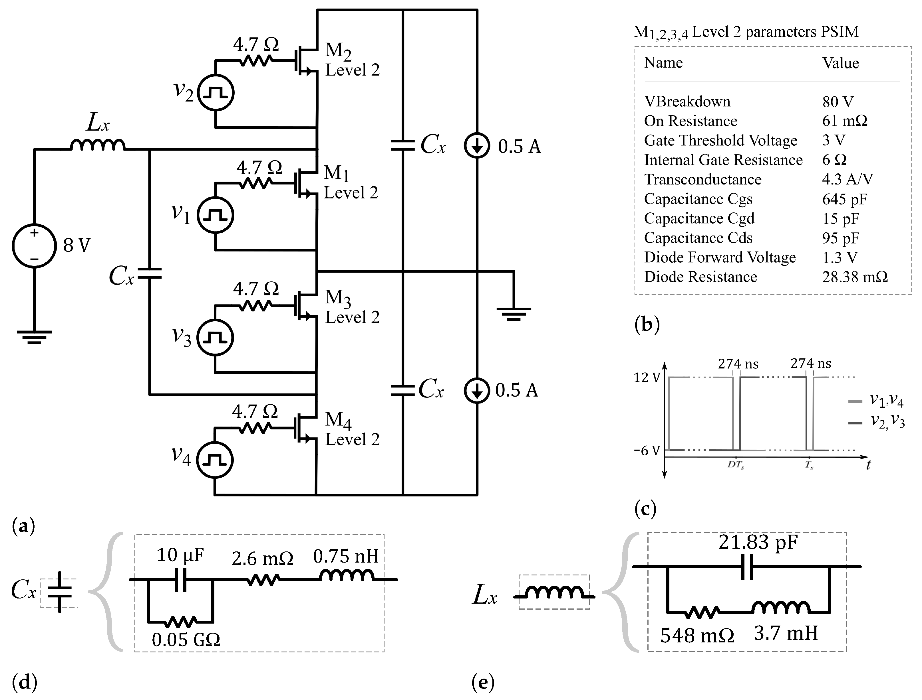
| Variable | Case Study | Vin [V] | C [μF] | L [mH] | Ix [A] | D [%] | Ts [μs] |
|---|---|---|---|---|---|---|---|
| Ripple | 1 | 5.0 | 100 | 37 | 1.0 | 50 | 50 |
| 2 | 5.0 | 10.0 | 3.7 | 1.0 | 50 | 50 | |
| Duty cycle | 3 | 3.0 | 10.0 | 3.7 | 0.2 | 10 | 50 |
| 4 | 3.0 | 10.0 | 3.7 | 0.2 | 30 | 50 | |
| 5 | 3.0 | 10.0 | 3.7 | 0.2 | 50 | 50 | |
| 6 | 3.0 | 10.0 | 3.7 | 0.2 | 70 | 50 | |
| 7 | 3.0 | 10.0 | 3.7 | 0.2 | 90 | 50 | |
| Input voltage | 8 | 6.0 | 10.0 | 3.7 | 1.0 | 50 | 50 |
| 9 | 7.0 | 10.0 | 3.7 | 1.0 | 50 | 50 | |
| 10 | 8.0 | 10.0 | 3.7 | 1.0 | 50 | 50 | |
| 11 | 9.0 | 10.0 | 3.7 | 1.0 | 50 | 50 | |
| 12 | 10 | 10.0 | 3.7 | 1.0 | 50 | 50 |
| Case Study | Ripple | Simulation Time [min] | ||
|---|---|---|---|---|
| OrCAD | LTspice | PSIM | ||
| 1 | Low | 542.9 | 399.6 | 4.500 |
| 2 | High | 8.500 | 6.900 | 4.700 |
| Case Study | Ripple | Simulator | [V] | [V] | [V] | [A] | [V] | [V] | [V] | [A] | Max. Error Parameter |
|---|---|---|---|---|---|---|---|---|---|---|---|
| 1 | Low | T | 10.02 | 9.828 | 9.938 | 2.000 | 0.188 | 0.188 | 0.250 | 0.003 | |
| S1 | 9.903 | 9.690 | 9.831 | 1.998 | 0.164 | 0.174 | 0.250 | 0.003 | |||
| S2 | 9.992 | 9.779 | 9.920 | 2.006 | 0.165 | 0.175 | 0.252 | 0.003 | |||
| S3 | 10.00 | 9.789 | 9.929 | 2.000 | 0.164 | 0.174 | 0.250 | 0.003 | |||
| Error [mA] o [mV] | 113.1 | 137.9 | 106.7 | 6.400 | 23.40 | 13.30 | 1.600 | 0.000 | |||
| Error [%] | 1.129 | 1.403 | 1.074 | 0.320 | 12.48 | 7.093 | 0.640 | 0.000 | |||
| 2 | High | T | 10.16 | 8.281 | 9.375 | 2.000 | 1.875 | 1.875 | 2.500 | 0.034 | |
| S1 | 10.18 | 8.280 | 9.404 | 1.996 | 1.836 | 1.859 | 2.500 | 0.034 | |||
| S2 | 10.06 | 8.154 | 9.283 | 2.003 | 1.841 | 1.861 | 2.509 | 0.034 | |||
| S3 | 10.08 | 8.179 | 9.305 | 1.999 | 1.834 | 1.856 | 2.500 | 0.034 | |||
| Error [mA] o [mV] | 97.30 | 127.1 | 92.30 | 4.500 | 40.90 | 18.80 | 8.500 | 0.600 | |||
| Error [%] | 0.958 | 1.535 | 0.985 | 0.225 | 2.181 | 1.003 | 0.340 | 1.775 |
| Ripple | ||||||||||||||||
|---|---|---|---|---|---|---|---|---|---|---|---|---|---|---|---|---|
| MAPE [%] | SD [%] | MAPE [%] | SD [%] | MAPE [%] | SD [%] | MAPE [%] | SD [%] | MAPE [%] | SD [%] | MAPE [%] | SD [%] | MAPE [%] | SD [%] | MAPE [%] | SD [%] | |
| Low | 0.504 | 0.544 | 0.769 | 0.551 | 0.445 | 0.547 | 0.142 | 0.160 | 12.25 | 0.355 | 6.880 | 0.282 | 0.213 | 0.370 | 0.000 | 0.000 |
| High | 0.640 | 0.384 | 0.931 | 0.804 | 0.681 | 0.340 | 0.133 | 0.098 | 2.020 | 0.199 | 0.862 | 0.132 | 0.120 | 0.191 | 0.690 | 0.951 |
| Case Study | D [%] | Simulator | [V] | [V] | [V] | [A] | [V] | [V] | [V] | [A] | Max. Error Parameter |
|---|---|---|---|---|---|---|---|---|---|---|---|
| 3 | 10 | T | 3.345 | 2.770 | 3.298 | 0.222 | 0.275 | 0.475 | 0.500 | 0.004 | |
| S3 | 3.342 | 2.763 | 3.297 | 0.222 | 0.271 | 0.471 | 0.500 | 0.004 | |||
| Error [mA] o [mV] | 2.605 | 6.916 | 1.556 | 0.027 | 4.274 | 3.913 | 0.003 | 0.017 | |||
| Error [%] | 0.078 | 0.250 | 0.047 | 0.012 | 1.554 | 0.824 | 0.001 | 0.409 | |||
| 4 | 30 | T | 4.312 | 3.837 | 4.196 | 0.286 | 0.325 | 0.425 | 0.500 | 0.012 | |
| S3 | 4.307 | 3.827 | 4.192 | 0.286 | 0.319 | 0.421 | 0.500 | 0.012 | |||
| Error [mA] o [mV] | 4.772 | 10.11 | 3.634 | 0.077 | 5.949 | 3.819 | 0.001 | 0.025 | |||
| Error [%] | 0.111 | 0.263 | 0.087 | 0.027 | 1.830 | 0.899 | 0.000 | 0.208 | |||
| 5 | 50 | T | 6.031 | 5.656 | 5.875 | 0.400 | 0.375 | 0.375 | 0.500 | 0.020 | |
| S3 | 6.021 | 5.640 | 5.866 | 0.400 | 0.367 | 0.371 | 0.500 | 0.020 | |||
| Error [mA] o [mV] | 10.24 | 16.35 | 9.013 | 0.115 | 8.361 | 3.703 | 0.010 | 0.037 | |||
| Error [%] | 0.170 | 0.289 | 0.153 | 0.029 | 2.230 | 0.987 | 0.002 | 0.184 | |||
| 6 | 70 | T | 10.03 | 9.751 | 9.860 | 0.667 | 0.425 | 0.325 | 0.500 | 0.028 | |
| S3 | 10.00 | 9.719 | 9.837 | 0.667 | 0.413 | 0.321 | 0.500 | 0.028 | |||
| Error [mA] o [mV] | 23.83 | 31.91 | 22.53 | 0.096 | 12.36 | 3.606 | 0.016 | 0.078 | |||
| Error [%] | 0.238 | 0.327 | 0.229 | 0.014 | 2.908 | 1.110 | 0.003 | 0.275 | |||
| 7 | 90 | T | 30.01 | 29.84 | 29.87 | 2.000 | 0.475 | 0.275 | 0.500 | 0.036 | |
| S3 | 29.81 | 29.61 | 29.66 | 2.000 | 0.456 | 0.272 | 0.500 | 0.036 | |||
| Error [mA] o [mV] | 202.5 | 223.2 | 201.1 | 0.147 | 18.79 | 3.455 | 0.102 | 0.259 | |||
| Error [%] | 0.675 | 0.748 | 0.673 | 0.007 | 3.955 | 1.256 | 0.020 | 0.709 |
| Case Study | ||||||||||||||||
|---|---|---|---|---|---|---|---|---|---|---|---|---|---|---|---|---|
| MAPE [%] | SD [%] | MAPE [%] | SD [%] | MAPE [%] | SD [%] | MAPE [%] | SD [%] | MAPE [%] | SD [%] | MAPE [%] | SD [%] | MAPE [%] | SD [%] | MAPE [%] | SD [%] | |
| 3 to 7 | 0.254 | 0.243 | 0.376 | 0.210 | 0.238 | 0.253 | 0.018 | 0.009 | 2.496 | 0.962 | 1.015 | 0.172 | 0.005 | 0.009 | 0.357 | 0.215 |
| Case Study | [V] | Simulator | [V] | [V] | [V] | [A] | [V] | [V] | [V] | [A] | Max. Error Parameter |
|---|---|---|---|---|---|---|---|---|---|---|---|
| 8 | 6 | T | 12.16 | 10.28 | 11.38 | 2.000 | 1.875 | 1.875 | 2.500 | 0.041 | |
| S3 | 12.11 | 10.21 | 11.34 | 1.999 | 1.834 | 1.856 | 2.500 | 0.040 | |||
| Error [mA] o [mV] | 45.98 | 73.03 | 39.74 | 0.679 | 41.19 | 18.74 | 0.132 | 0.190 | |||
| Error [%] | 0.378 | 0.710 | 0.349 | 0.034 | 2.197 | 1.000 | 0.005 | 0.469 | |||
| 9 | 7 | T | 14.16 | 12.28 | 13.38 | 2.000 | 1.875 | 1.875 | 2.500 | 0.047 | |
| S3 | 14.11 | 12.21 | 13.34 | 1.999 | 1.834 | 1.856 | 2.500 | 0.047 | |||
| Error [mA] o [mV] | 43.89 | 71.45 | 37.72 | 0.555 | 41.21 | 18.82 | 0.026 | 0.203 | |||
| Error [%] | 0.310 | 0.582 | 0.282 | 0.028 | 2.198 | 1.004 | 0.001 | 0.430 | |||
| 10 | 8 | T | 16.16 | 14.28 | 15.38 | 2.000 | 1.875 | 1.875 | 2.500 | 0.054 | |
| S3 | 16.11 | 14.21 | 15.34 | 1.999 | 1.834 | 1.856 | 2.500 | 0.054 | |||
| Error [mA] o [mV] | 44.26 | 72.20 | 38.10 | 0.554 | 41.28 | 18.79 | 0.026 | 0.204 | |||
| Error [%] | 0.274 | 0.506 | 0.248 | 0.028 | 2.202 | 1.002 | 0.001 | 0.377 | |||
| 11 | 9 | T | 18.16 | 16.28 | 17.38 | 2.000 | 1.875 | 1.875 | 2.500 | 0.061 | |
| S3 | 18.11 | 16.21 | 17.34 | 1.999 | 1.834 | 1.856 | 2.500 | 0.061 | |||
| Error [mA] o [mV] | 44.64 | 72.95 | 38.48 | 0.554 | 41.36 | 18.76 | 0.025 | 0.204 | |||
| Error [%] | 0.246 | 0.448 | 0.221 | 0.028 | 2.206 | 1.000 | 0.001 | 0.335 | |||
| 12 | 10 | T | 20.16 | 18.28 | 19.38 | 2.000 | 1.875 | 1.875 | 2.500 | 0.068 | |
| S3 | 20.11 | 18.21 | 19.34 | 1.999 | 1.834 | 1.856 | 2.500 | 0.067 | |||
| Error [mA] o [mV] | 45.01 | 73.70 | 38.86 | 0.553 | 41.43 | 18.72 | 0.024 | 0.204 | |||
| Error [%] | 0.223 | 0.403 | 0.201 | 0.028 | 2.210 | 0.999 | 0.001 | 0.301 |
| Case Study | ||||||||||||||||
|---|---|---|---|---|---|---|---|---|---|---|---|---|---|---|---|---|
| MAPE [%] | SD [%] | MAPE [%] | SD [%] | MAPE [%] | SD [%] | MAPE [%] | SD [%] | MAPE [%] | SD [%] | MAPE [%] | SD [%] | MAPE [%] | SD [%] | MAPE [%] | SD [%] | |
| 8 to 12 | 0.291 | 0.055 | 0.540 | 0.109 | 0.265 | 0.053 | 0.029 | 0.003 | 2.212 | 0.027 | 1.003 | 0.004 | 0.002 | 0.002 | 0.389 | 0.059 |
| Case Study | All Variables | |||||
|---|---|---|---|---|---|---|
| MAPE [%] | SD [%] | MAPE [%] | SD [%] | MAPE [%] | SD [%] | |
| 1 to 2 | 0.425 | 0.447 | 2.929 | 4.529 | 1.677 | 3.367 |
| 3 to 7 | 0.221 | 0.230 | 0.968 | 1.081 | 0.595 | 0.859 |
| 8 to 12 | 0.281 | 0.195 | 0.902 | 0.859 | 0.591 | 0.690 |
| All cases | 0.280 | 0.267 | 1.267 | 1.267 | 0.774 | 1.566 |
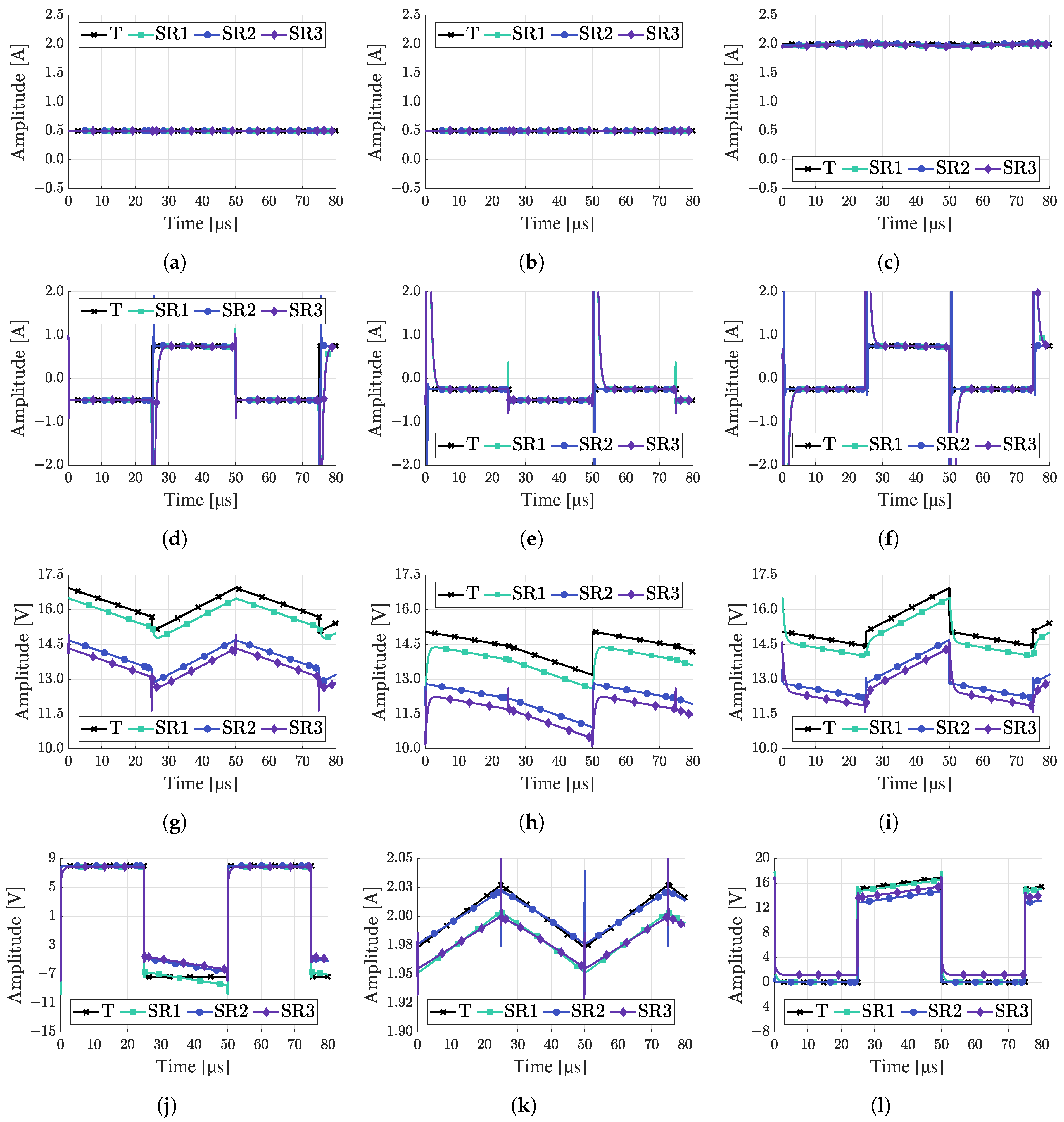
| Case Study | Simulation Type | [V] | [V] | [V] | [A] | [V] | [V] | [V] | [A] | Max. Error Parameter |
|---|---|---|---|---|---|---|---|---|---|---|
| T | 16.16 | 14.28 | 15.38 | 2.000 | 1.875 | 1.875 | 2.500 | 0.054 | ||
| 10 | SR1 | 15.72 | 13.66 | 14.97 | 1.978 | 1.689 | 1.795 | 2.500 | 0.052 | |
| Error [mA] o [mV] | 439.4 | 618.3 | 409.7 | 22.19 | 186.1 | 80.32 | 0.050 | 1.817 | ||
| Error [%] | 2.720 | 4.330 | 2.665 | 1.109 | 9.928 | 4.284 | 0.002 | 3.362 | ||
| SR2 | 13.92 | 12.02 | 13.14 | 2.000 | 1.851 | 1.898 | 2.503 | 0.047 | ||
| Error [mA] o [mV] | 2237 | 2266 | 2230 | 0.497 | 24.48 | 23.27 | 2.563 | 7.416 | ||
| Error [%] | 13.85 | 15.87 | 14.51 | 0.025 | 1.305 | 1.241 | 0.103 | 13.72 | ||
| SR3 | 13.57 | 11.52 | 12.82 | 1.978 | 1.680 | 1.780 | 2.490 | 0.044 | ||
| Error [mA] o [mV] | 2584 | 2763 | 2554 | 22.16 | 195.0 | 95.00 | 10.00 | 10.05 | ||
| Error [%] | 15.99 | 19.35 | 16.61 | 1.108 | 10.40 | 5.067 | 0.400 | 18.60 |
Publisher’s Note: MDPI stays neutral with regard to jurisdictional claims in published maps and institutional affiliations. |
© 2021 by the authors. Licensee MDPI, Basel, Switzerland. This article is an open access article distributed under the terms and conditions of the Creative Commons Attribution (CC BY) license (https://creativecommons.org/licenses/by/4.0/).
Share and Cite
Casallas, I.; Urbina, R.; Paez-Rueda, C.-I.; Correa-Flórez, C.A.; Vuelvas, J.; Parraga, M.; Hay, A.-K.; Fajardo, A.; Perilla, G. A Novel Single-Inductor Bipolar-Output DC/DC Boost Converter for OLED Microdisplays. Energies 2021, 14, 6220. https://doi.org/10.3390/en14196220
Casallas I, Urbina R, Paez-Rueda C-I, Correa-Flórez CA, Vuelvas J, Parraga M, Hay A-K, Fajardo A, Perilla G. A Novel Single-Inductor Bipolar-Output DC/DC Boost Converter for OLED Microdisplays. Energies. 2021; 14(19):6220. https://doi.org/10.3390/en14196220
Chicago/Turabian StyleCasallas, Ingrid, Robert Urbina, Carlos-Ivan Paez-Rueda, Carlos Adrián Correa-Flórez, José Vuelvas, Manuel Parraga, Abdel-Karim Hay, Arturo Fajardo, and Gabriel Perilla. 2021. "A Novel Single-Inductor Bipolar-Output DC/DC Boost Converter for OLED Microdisplays" Energies 14, no. 19: 6220. https://doi.org/10.3390/en14196220
APA StyleCasallas, I., Urbina, R., Paez-Rueda, C.-I., Correa-Flórez, C. A., Vuelvas, J., Parraga, M., Hay, A.-K., Fajardo, A., & Perilla, G. (2021). A Novel Single-Inductor Bipolar-Output DC/DC Boost Converter for OLED Microdisplays. Energies, 14(19), 6220. https://doi.org/10.3390/en14196220