Abstract
Many applications (electric vehicles, renewable energies, low-voltage DC grids) require simple, high-power density and low-current ripple-boost converters. Traditional step-up converters are limited when large transformation ratios are involved. In this work is proposed a step-up converter that brings together the characteristics of high gain, low ripple, and high-power density. From the converter proposal, a mathematical analysis of its operation is first performed, including its static transfer function, stress of components, and voltage and current ripples. Furthermore, it provides a design example for an application of Vin = 48 V to Vo = 270 V and 500 W. For its implementation, two different wide bandgap (WBG) semiconductor models have been used, hybrid GaN cascodes and SiC MOSFETs. Finally, the experimental results of the produced prototypes are shown, and the results are discussed.
1. Introduction
In recent years, with the massive adoption of electricity as the main energy source by end users, an adaptation in voltage ratings is taking place for distribution as well as for consumption.
At the domestic and industrial level, the main promoters of change are the introduction of low-voltage direct-current (LVDC) distribution grids and the increasing use of renewable sources of energy. In this field, the proposed distribution and consumption network voltages are in the 24–380 V range [1,2,3,4,5,6,7]. Based on the premise that the output voltages of renewable energy sources—photovoltaic and fuel cells—are below the voltage distribution and consumption level, the use of boost converters is required [8,9,10].
Within the automotive sector, the latest electric vehicle configurations operate in general in the 150–450 Vdc range [11], requiring, as well, the use of step-up converters to supply voltage to the electrical engines from the batteries or to charge them [12].
The aerospace and aeronautical segments do the same. The introduction of electric propulsion systems and the transition from mechanical to electric drive systems have increased electric power consumption, thus increasing the need to use higher voltage [13,14,15,16].
In this scenario, DC–DC conversion systems play a key part, allowing the interconnection between buses and loads from energy sources.
The expected features of such converters are reliability, size, weight, and reduced current ripple. Input current ripple is particularly important in those systems where the power source is a battery or fuel cell, because of its lifetime impact [17].
To solve these requirements, different solutions can be considered taking into account the simplicity of design, implementation, and cost. In the previous mentioned applications, non-isolated interleaved boost converters are widely used [10]. Nevertheless, there are other applications, usually related with high step-up ratios and high power, where efficiency is a major concern. Here, isolated converters are used in order to optimize efficiency and enhance the security of the system thanks to the transformer, but in counterpart volume, mass and price are increased [18,19].
A key factor in the converter selection topology is the step-up ratio. High step-up ratios using simple converters and controllers is a challenging task due to the presence of zeros in the left half-plane. This tends to unbalance the system when it operates at high duty cycles, becoming the controller more sensitive to inaccuracies and delays [20].
Although there are techniques described in the literature to minimize these effects [21,22], the use of voltage boosting techniques allows lower duty cycles, reducing the controllers complexity but at the same time increasing the number of components [23].
Low duty cycle enables simpler multidevice structures in the converters, providing several advantages: decouple the switching frequency from the inductor frequency, reduce the input current ripple, share the losses among devices and in more complex designs, enable reconfiguration techniques to improve the versatility and robustness of the converter [24].
Voltage boosting techniques can be used to reduce the duty cycle; the most popular are based on charge pumps that are well-suited for low power applications [25], the use of voltage multiplication cells that require the use of capacitors [26], and finally the use of switched inductors, based on magnetizing inductors in parallel and demagnetizing them in series [27]. In this paper, the use of switched inductors will be analyzed.
In [28] a high-gain (from 32 to 800 V), non-isolated step-up converter with interleaving is introduced. It employs voltage multiplication cells to keep a reduced duty cycle of 0.68. The converter has been evaluated in different load conditions achieving a 95% efficiency for 500 W. Another high-gain (from 20 to 260 V), non-isolated converter is presented in [29]. It uses transistor-switched inductors to achieve a reduced duty cycle of 0.75. For experimental validation, it has been evaluated at 200 W loads, achieving 94.5% efficiency.
This work proposes a high-gain interleaving boost converter scheme that uses a switched inductor for achieving high gain ratios with no need of high duty cycles. As mentioned, the switched inductor structure charges several inductors in parallel during the ON-State and discharges them in series during OFF-State.
The main strength of this proposal lies in its great versatility. A widespread structure of n interleaved phases, k phase-switched inductors and m phase-switched power transistors is developed. This allows the optimization of the inductors, the limitation of the input and output current ripple and power sharing between phases.
Considering the high step-up ratio required and with the aim of increasing power density, the prototypes have been fully developed with wide bandgap (WBG) semiconductors. The key advantages of these semiconductors -SiC and GaN- over traditional silicon devices are the Band Gap Energy, Breakdown Field, Saturation Drift Velocity and Thermal conductivity. As a result, higher voltage transistors can be produced for higher temperatures, which enables the optimization of thermal management systems—and higher frequency—which reduces the size of the passive elements [30,31,32,33].
To conclude this introduction, the paper has been structured as follows: Section 2 presents the general topology and its working concept. In Section 3, two converters are proposed, one based on SiC switches and one based on GaN switches. Section 4 presents and discusses the experimental results, and it closes with a conclusion of the work in Section 5.
2. Converter Description and Operation Principle
The proposed converter scheme has a multiphase high-gain boost (HGBoost) structure, as shown in Figure 1a. The benefits of this type of structure, commonly referred to as the Interleaved Boost Converter (IBC), are related to the power-sharing between phases and the reduction of the input current ripple [34,35].
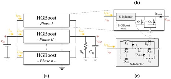
Figure 1.
Simplified sketch of the proposed high-gain boost converter: (a) General diagram of the n-phase converter; (b) Single-phase scheme with m transistors; (c) Scheme of the selected switched inductor.
According to Figure 1b, the proposal employs multiple switches per phase. The switches will turn on sequentially every 360°/m, where m is the number of switches per phase, sharing the power between all each period. On the other hand, there will be a phase shift of 360°/n, where n is the number of phases. There is an impact of this type of implementation in terms of power and current distribution between switches. The main drawback of this type of implementation is the increased complexity of the control [10].
Additionally, the proposed converter incorporates a switched inductor cell (S-Inductor) that improves the step-up voltage capability of the circuit.
A continuous current mode operation (CCM) would be considered for the HGBoost operating description [36]. Each HGBoost phase has two states, ON-State and OFF-State (Figure 2). The voltage and current waveforms in each inductor of the S-Inductor based on each of the following states is shown in Figure 3a. It is important to note that due to the interleaving, the duty cycle (D) will be within the range (0, 1/m), where m is the number of switches per phase.
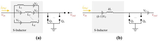
Figure 2.
HGBoost equivalent states: (a) ON-State. (b) OFF-State.
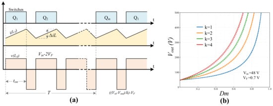
Figure 3.
Waveforms and graphic transfer function: (a) Current and voltage waveforms in an inductor (L) of one inductor from S-Inductor. (b) Graphic DC transfer function representation (VO) for different numbers of inductors of the S-Inductor (k). An input voltage of 48 V and a direct diode drop (VF) of 0.7 V are considered. In continuous line, the drop voltage of the diodes is neglected, in dashed line, a 0.7 V voltage drop is considered.
In the ON-state, one of the transistors is turned on. Because of the S-Inductor configuration, during this interval, shown in Figure 2a, the k-inductors are connected in parallel. A small unbalance voltage appears in the inductors in parallel; the first inductor and the k-th have only one diode (Dp) in series (VF) in this state, thus they have a slightly higher voltage according to the expression (1).
During the OFF-State all transistors are off and the current flows through the series diodes (DS), keeping them in series and supplying the load through the output diode (DO), according to Figure 2b. The voltage in each inductor, assuming an identical charging in ON-State of the inductors is given by (2).
Assuming identical inductances, the following DC transfer function (3) can be obtained, where D means the one-switch duty cycle, vin the input voltage, vout the output voltage, m the number of switches per phase and k the total number of inductors in the S-inductor. A graphic representation of the output voltage as a function of Dm for an input voltage of 48 V and different k is shown in Figure 3b.
The stress on the semiconductors will be analyzed next. The blocking voltage supported by the parallel diodes of the S-Inductor (Dpi,j—Figure 1c) are described in (4) and (5). It should be noted that the Dpi,1 diode is connected to the input and the Dpi,2 diodes are connected to the output. In all cases VF was neglected compared to the magnitude of the input and output voltages. The maximum blocking voltage in the series diode (Dsi) of the S-Inductor is described by (6).
On the other hand, the maximum voltages supported by the switches correspond to the output voltage .
For the inductor current, it is possible to calculate, assuming no losses, an average current per inductor defined by (7) where n is the number of phases and io the output current.
Maximum diode current corresponds with the maximum inductor current, defined according to (8). Maximum switch current is defined by (9) where f is the switching frequency.
As mentioned before, an advantage of interleaving topologies is the decreasing of current ripple, (10) and (11) are the expressions for input and output current ripple are described, where and .
3. Converter Design Example
The prototype for experimental validation is a two-phase device (n = 2), with two switches per phase (m = 2) and two inductors per phase (k = 2). The voltage gain is Vo/Vin = 5.6, with Vin = 48 V and Vout = 270 V. Based on (3), this implies a switch duty cycle of 0.35. This voltage range is well-suited for a large number of applications [1,5,37,38,39].
Because of the high output voltage, full WBG diodes and switches have been considered. In both cases, the diodes are SiC, but SiC and GaN switches have been tested. In addition, Schottky SiC diodes minimize switching losses and make it possible to increase the switching frequency compared to silicon diodes [30].
SiC and GaN switches, due to the high voltage breaking field, can be produced using thinner wafers—compared to Si—achieving significant reductions in resistances (Ron) and parasitic capacitances. In practice, this means lower switching losses [31] and also lower conduction losses, enabling the reduction of thermal management systems and increasing power density [32].
A major constraint for this use is the special driving characteristics required. On one hand, the low capacitances of the devices (Ciss, Coss, Crss) require layouts with minimum source inductance in order to minimize the ringing on switching [40,41]. Furthermore, and especially for GaN devices, they have a high sensitivity to gate overvoltages [40]. The latest SiC switch (MOSFET) reviews incorporate dedicated source terminals to minimize the effects of source inductance on switching [42]. Due to their gate-overvoltage sensitivity, some GaN switch manufacturers integrate transistor and controller on the same chip [43]; however, currently these devices are for 300 V and are therefore not suitable for this application.
To achieve the GaN device advantages without the driver disadvantage, hybrid devices were considered. A GaN cascode hybrid switch uses a GaN Junction Field-Effect Transistor (JFET) as the main power control device, while a conventional low-voltage Si MOSFET is used to control it. Consequently, very balanced devices in terms of performance/drive requirements are available in the market.
The developed prototype to validate the proposal is shown in Figure 4, and the selected elements are in Table 1. To drive both transistor proposals (TP65H035WSQA and SCT3120ALHR), CREE’s CPWR-AN10 driver was used. One of the advantages of this driver lies in the use of unregulated isolation sources to provide controlled ON and OFF voltages to the transistors [44] allowing the validation of both transistors without major layout changes. The manufacturers’ recommended driving voltages were used [45,46]. The CPWR-AN10 includes an optoisolated inputs control, and a Zynq®-7000 Xilinx unit was used to generate the PWM control signals.
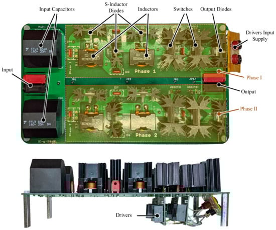
Figure 4.
Top and side view of the prototype circuit.

Table 1.
Parameters and elements selected in the prototypes.
4. Experimental Results: SiC and GaN Versions
A MDO3104 Tektronix mixed-domain oscilloscope was used as a data acquisition instrument. Tektronix TCP0030A current probes and Tektronix THDP0200 high-voltage differential probes were also used.
For its operation, the converter was controlled in open loop, through a fixed duty cycle (D = 0.35) for a constant output voltage. The same measurements were carried out using SiC and GaN switches.
4.1. Phase Currents and Switch Voltages
The phase current and the drain-source switch voltage waveforms are shown in Figure 5a for the SiC converter and Figure 5b for the GaN converter.
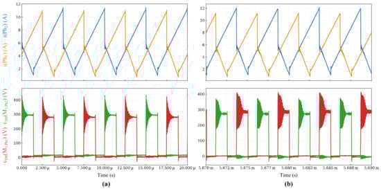
Figure 5.
Converter waveforms: (a) SiC switch converter (SCT3120ALHR). Upper waveform: In orange current i(Ph1) (2 A/div); in blue i(Ph2) (2 A/div). Lower waveform: In green VDS(M1,Ph1) (100 V/div); in red VDS(M1,Ph2) (100 V/div). Time scale 2.5 µs/div. (b) GaN switch converter (TP65H035WSQA). Upper waveform: In orange current i(Ph1) (2 A/div); in blue i(Ph2) (2 A/div). Lower waveform: In green VDS(M1,Ph1) (100 V/div); in red VDS(M1,Ph2) (100 V/div). Time scale 2.5 µs/div.
First, correct phase interleaving is verified. For the SiC converter, Figure 5a, a properly balanced current is verified, with a maximum current of roughly 11.3 A; this value has good correlation with (8), assuming identical inductors. In the GaN converter Figure 5b, there are 400 mA maximum current variations per phase; this may be due to the tolerance of the inductors (15%).
By means of a voltage analysis of the switches, the DC transfer function (3) is verified, as well as the output voltage, since .
On the other hand, some switching ringing appears, due to resonances between the parasitic elements of the circuit [47]. However, the ringing overvoltage is within the nominal voltage of the switches (650 V) and does not represent a risk.
4.2. Output Currents and Output Diode Voltage
Figure 6 shows the converter output current (iout) waveform before the output capacitor (Co) and the single-phase output diodes voltages as well as the drain-source switch voltage for SiC Figure 5a and GaN Figure 5b prototypes.
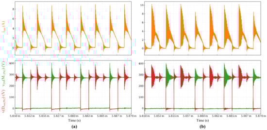
Figure 6.
Converter waveforms: (a) SiC switch converter (SCT3120ALHR). Upper waveform: In orange current iout (2 A/div). Lower waveform: In green VDS(M1,Ph2) (100 V/div); in red V(Dout,Ph2) (100 V/div). Time scale 2.5 µs/div. (b) GaN switch converter (TP65H035WSQA). Upper waveform: In orange current iout (2 A/div). Lower waveform: In green VDS(M1,Ph2) (100 V/div); in red V(Dout,Ph2) (100 V/div) Time scale 2.5 µs/div.
It can be noted that the output current frequency equals twice the frequency from one switch, allowing it to reduce the voltage and current ripple.
The inductor tolerance effects are shown more clearly in the GaN prototype again in Figure 6b; however, these currents are within the range of the output diodes (UJ2D1210T).
4.3. Inductor Currents
Figure 7 shows the first inductor current of each S-Inductor, Figure 7a for the SiC converter and Figure 7b for the GaN converter. It can be verified that both converters work in continuous mode with about 500 mA of margin. The maximum currents reached are in accordance with the theoretical value (8), at 5.6 A value.
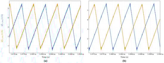
Figure 7.
Converter waveforms: (a) SiC switch converter (SCT3120ALHR). In orange current i(L1,Ph1) (2 A/div); in blue i(L1,Ph1) (2 A/div). Time scale 2 µs/div. (b) GaN switch converter (TP65H035WSQA). In orange current i(L1,Ph1) (2 A/div); in blue i(L1,Ph1) (2 A/div). Time scale 2 µs/div.
4.4. Efficiency
Figure 8 shows the efficiency of the prototypes under different load conditions, 156 Ω and 94 Ω. For its operation, a fixed 0.35 duty cycle was selected and an input voltage sweep between 12 and 48 V was performed, regardless of the type of semiconductor employed (SiC & GaN).
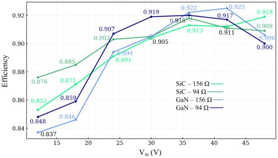
Figure 8.
Prototypes efficiency under different load and input voltage. In light green SiC prototype with 156 Ω load. In dark green SiC prototype with 94 Ω load. In light blue GaN prototype with 156 Ω load. In dark blue GaN prototype with 94 Ω load.
5. Conclusions
An interleaved high-gain boost converter based on a switched inductor able to provide high-gain ratio for operation in low-voltage DC networks and automotive power systems has been presented and validated in this paper. The main advantage of the proposal is its high versatility, allowing power sharing between phases and switches, and reducing the current ripple.
The equations provide three adjusting parameters, m (number of switches per phase), k (number of switched inductors per phase), and n (number of phases). Thanks to its high level of configurability, the proposal’s design can cover a wide range of step-up voltages and power ratings.
For its validation, two 500 W converters with 48Vin and 270Vo were designed; a two-phase device (n = 2), with two switches per phase (m = 2) and two inductors per phase (k = 2) were selected.
The experimental results based on the use of SiC and GaN switches show very uniform results from the point of view of switching response as well as efficiency. Since the evaluated WBG devices have different driving voltages, the use of an adjustable voltage driver (CPWR-AN10) was possible to validate the design with both switches without driver changes.
For future works, it would be interesting to evaluate the operation using soft switching techniques to increase efficiency and to suggest synchronous rectification techniques to minimize the impact of the diodes.
Author Contributions
D.M., A.G. and J.M.B. conceived the idea, designed the experiment, guided the experiment, and wrote the manuscript; R.G., C.T. and C.O. conducted most of the validation test. All authors have read and agreed to the published version of the manuscript.
Funding
This research received no external funding.
Institutional Review Board Statement
Not applicable.
Informed Consent Statement
Not applicable.
Data Availability Statement
Not applicable.
Conflicts of Interest
The authors declare no conflict of interest.
References and Notes
- Rodriguez-Diaz, E.; Savaghebi, M.; Vasquez, J.C.; Guerrero, J.M. An overview of low voltage DC distribution systems for residential applications. In Proceedings of the 2015 IEEE 5th International Conference on Consumer Electronics—Berlin (ICCE-Berlin), Berlin, Germany, 6–9 September 2015; pp. 318–322. [Google Scholar]
- Elvira, D.G.; Blaví, H.V.; Pastor, À.C.; Salamero, L.M. Efficiency Optimization of a Variable Bus Voltage DC Microgrid. Energies 2018, 11, 3090. [Google Scholar] [CrossRef]
- EATON Impact DC-grids. 2018. Available online: https://gelijkspanning.org/wp-content/uploads/2020/06/2.6-GG-DC-presentatie-Eaton-Waarom-DC-Rev6E.pdf (accessed on 2 February 2021).
- Mackay, L.; van der Blij, N.H.; Ramirez-Elizondo, L.; Bauer, P. Toward the Universal DC Distribution System. Electr. Power Compon. Syst. 2017, 45, 1032–1042. [Google Scholar] [CrossRef]
- Dragicevic, T.; Lu, X.; Vasquez, J.C.; Guerrero, J.M. DC Microgrids—Part II: A Review of Power Architectures, Applications, and Standardization Issues. IEEE Trans. Power Electron. 2016, 31, 3528–3549. [Google Scholar] [CrossRef]
- Ravyts, S.; Van Den Broeck, G.; Hallemans, L.; Vecchia, M.D.; Driesen, J. Fuse-Based Short-Circuit Protection of Converter Controlled Low-Voltage DC Grids. IEEE Trans. Power Electron. 2020, 35, 11694–11706. [Google Scholar] [CrossRef]
- Ourahou, M.; Ayrir, W.; EL Hassouni, B.; Haddi, A. Review on smart grid control and reliability in presence of renewable energies: Challenges and prospects. Math. Comput. Simul. 2020. [Google Scholar] [CrossRef]
- Pan, C.T.; Lai, C.M. A high-efficiency high step-up converter with low switch voltage stress for fuel-cell system applications. IEEE Trans. Ind. Electron. 2010, 57, 1998–2006. [Google Scholar] [CrossRef]
- Li, W.; He, X. Review of Nonisolated High-Step-Up DC/DC Converters in Photovoltaic Grid-Connected Applications. IEEE Trans. Ind. Electron. 2011, 58, 1239–1250. [Google Scholar] [CrossRef]
- Garrigós, A.; Sobrino-Manzanares, F. Interleaved multi-phase and multi-switch boost converter for fuel cell applications. Int. J. Hydrogen Energy 2015, 40, 8419–8432. [Google Scholar] [CrossRef]
- Kerler, M.; Burda, P.; Baumann, M.; Lienkamp, M. A concept of a high-energy, low-voltage EV battery pack. In Proceedings of the 2014 IEEE International Electric Vehicle Conference (IEVC), Florence, Italy, 17–19 December 2014; pp. 1–8. [Google Scholar]
- Deilami, S.; Muyeen, S.M. An insight into practical solutions for electric vehicle charging in smart grid. Energies 2020, 1545. [Google Scholar] [CrossRef]
- Buticchi, G.; Bozhko, S.; Liserre, M.; Wheeler, P.; Al-Haddad, K. On-Board Microgrids for the More Electric Aircraft—Technology Review. IEEE Trans. Ind. Electron. 2019, 66, 5588–5599. [Google Scholar] [CrossRef]
- Wheeler, P.; Bozhko, S. The More Electric Aircraft: Technology and challenges. IEEE Electrif. Mag. 2014, 2, 6–12. [Google Scholar] [CrossRef]
- De Boissieu, J.; Bouhours, G.; Boulanger, B.; Bourgue, O.; Meinguet, F.; Bekemans, M.; Cesaretti, G.; Taylor, R.; Bommottet, D.; Martens, P. High voltage electrical power system architecture optimized for electrical propulsion & high power payload. In Proceedings of the European Space Power Conference 2019, Juan-les-Pins, France, 30 September–4 October 2019; pp. 1–7. [Google Scholar]
- Bekemans, M.; Bronchart, F.; Scalais, T.; Franke, A. Configurable High Voltage Power Supply for Full Electric Propulsion Spacecraft. In Proceedings of the 2019 European Space Power Conference (ESPC 2019), Juan-les-Pins, France, 30 September–4 October 2019. [Google Scholar] [CrossRef]
- Khaligh, A.; Li, Z. Battery, Ultracapacitor, Fuel Cell, and Hybrid Energy Storage Systems for Electric, Hybrid Electric, Fuel Cell, and Plug-In Hybrid Electric Vehicles: State of the Art. IEEE Trans. Veh. Technol. 2010, 59, 2806–2814. [Google Scholar] [CrossRef]
- Liang, T.-J.; Lee, J.-H.; Chen, S.-M.; Chen, J.-F.; Yang, L.-S. Novel Isolated High-Step-Up DC–DC Converter with Voltage Lift. IEEE Trans. Ind. Electron. 2013, 60, 1483–1491. [Google Scholar] [CrossRef]
- Forouzesh, M.; Baghramian, A. Galvanically isolated high gain Y-source DC-DC converters for dispersed power generation. IET Power Electron. 2016, 9, 1192–1203. [Google Scholar] [CrossRef]
- Freudenberg, J.; Looze, D. Right half plane poles and zeros and design tradeoffs in feedback systems. IEEE Trans. Automat. Contr. 1985, 30, 555–565. [Google Scholar] [CrossRef]
- Bag, S.; Roy, T.; Mukhopadhyay, S.; Samanta, S.; Sheehan, R. Boost converter control using Smith Predictor technique to minimize the effect of Right Half Plane zero. Proc. IEEE Int. Conf. Control Appl. 2013, 983–988. [Google Scholar] [CrossRef]
- Wu, W.-C.; Bass, R.M.; Yeargan, J.R. Eliminating the effects of the right-half plane zero in fixed frequency boost converters. In Proceedings of the PESC 98 Record. In Proceedings of the 29th Annual IEEE Power Electronics Specialists Conference (Cat. No.98CH36196), Fukuoka, Japan, 22 May 1998; Volume 1, pp. 362–366. [Google Scholar]
- Forouzesh, M.; Siwakoti, Y.P.; Gorji, S.A.; Blaabjerg, F.; Lehman, B. Step-Up DC-DC converters: A comprehensive review of voltage-boosting techniques, topologies, and applications. IEEE Trans. Power Electron. 2017, 32, 9143–9178. [Google Scholar] [CrossRef]
- Sobrino-Manzanares, F.; Garrigos, A. Bidirectional, Interleaved, Multiphase, Multidevice, Soft-Switching, FPGA-Controlled, Buck–Boost Converter with PWM Real-Time Reconfiguration. IEEE Trans. Power Electron. 2018, 33, 9710–9721. [Google Scholar] [CrossRef]
- Palumbo, G.; Pappalardo, D. Charge Pump Circuits: An Overview on Design Strategies and Topologies. IEEE Circuits Syst. Mag. 2010, 10, 31–45. [Google Scholar] [CrossRef]
- Prudente, M.; Pfitscher, L.L.; Emmendoerfer, G.; Romaneli, E.F.; Gules, R. Voltage Multiplier Cells Applied to Non-Isolated DC–DC Converters. IEEE Trans. Power Electron. 2008, 23, 871–887. [Google Scholar] [CrossRef]
- Axelrod, B.; Berkovich, Y.; Ioinovici, A. Switched-Capacitor/Switched-Inductor Structures for Getting Transformerless Hybrid DC–DC PWM Converters. IEEE Trans. Circuits Syst. I Regul. Pap. 2008, 55, 687–696. [Google Scholar] [CrossRef]
- Alghaythi, M.L.; O’Connell, R.M.; Islam, N.E.; Khan, M.M.S.; Guerrero, J.M. A High Step-Up Interleaved DC-DC Converter with Voltage Multiplier and Coupled Inductors for Renewable Energy Systems. IEEE Access 2020, 8, 123165–123174. [Google Scholar] [CrossRef]
- Salvador, M.A.; Lazzarin, T.B.; Coelho, R.F. High Step-Up DC–DC Converter with Active Switched-Inductor and Passive Switched-Capacitor Networks. IEEE Trans. Ind. Electron. 2018, 65, 5644–5654. [Google Scholar] [CrossRef]
- Elasser, A.; Chow, T.P. Silicon carbide benefits and advantages for power electronics circuits and systems. Proc. IEEE 2002, 90, 969–986. [Google Scholar] [CrossRef]
- ON Semiconductors MOSFET Gate-Charge Origin and its Applications Introduction—2016.
- She, X.; Huang, A.Q.; Lucia, O.; Ozpineci, B. Review of Silicon Carbide Power Devices and Their Applications. IEEE Trans. Ind. Electron. 2017, 64, 8193–8205. [Google Scholar] [CrossRef]
- Matallana, A.; Ibarra, E.; López, I.; Andreu, J.; Garate, J.I.; Jordà, X.; Rebollo, J. Power module electronics in HEV/EV applications: New trends in wide-bandgap semiconductor technologies and design aspects. Renew. Sustain. Energy Rev. 2019, 113, 109264. [Google Scholar] [CrossRef]
- Hwang, J.C.; Chen, L.H.; Yeh, S.N. Comprehensive analysis and design of multi-leg fuel cell boost converter. Appl. Energy 2007, 84, 1274–1288. [Google Scholar] [CrossRef]
- Thounthong, P.; Davat, B. Study of a multiphase interleaved step-up converter for fuel cell high power applications. Energy Convers. Manag. 2010, 51, 826–832. [Google Scholar] [CrossRef]
- Erickson, R.W.; Maksimović, D. Fundamentals of Power Electronics; Springer US: Boston, MA, USA, 1997; ISBN 978-1-4757-0559-1. [Google Scholar]
- Rodriguez-Diaz, E.; Vasquez, J.C.; Guerrero, J.M. Intelligent DC Homes in Future Sustainable Energy Systems: When efficiency and intelligence work together. IEEE Consum. Electron. Mag. 2016, 5, 74–80. [Google Scholar] [CrossRef]
- Rodriguez-Diaz, E.; Chen, F.; Vasquez, J.C.; Guerrero, J.M.; Burgos, R.; Boroyevich, D. Voltage-Level Selection of Future Two-Level LVdc Distribution Grids: A Compromise Between Grid Compatibiliy, Safety, and Efficiency. IEEE Electrif. Mag. 2016, 4, 20–28. [Google Scholar] [CrossRef]
- Rodriguez-Diaz, E.; Vasquez, J.C.; Guerrero, J.M. Potential energy savings by using direct current for residential applications: A Danish household study case. In Proceedings of the 2017 IEEE Second International Conference on DC Microgrids (ICDCM), Atlanta, GA, USA, 27–29 June 2017; IEEE: Nuremburg, Germany, 2017; pp. 547–552. [Google Scholar]
- Lidow, A.; de Rooij, M.; Strydom, J.; Reusch, D.; Glaser, J. GaN Transistors for Efficient Power Conversion; John Wiley & Sons, Ltd.: Hoboken, NJ, USA, 2019; ISBN 9781119594406. [Google Scholar]
- Zhang, Z.; Fu, J.; Liu, Y.-F.; Sen, P.C. Switching Loss Analysis Considering Parasitic Loop Inductance with Current Source Drivers for Buck Converters. IEEE Trans. Power Electron. 2011, 26, 1815–1819. [Google Scholar] [CrossRef]
- CREE C3M0065100J—Datasheet. 2020.
- Efficient Power Conversion. EPC2112—Preliminary Datasheet. 2018.
- CREE CPWR-AN10—SiC MOSFET Driver. Rev-C—Datasheet. 2014.
- ROHM SCT3120ALHR—Datasheet. 2018.
- Transphorm Inc. TP65H035WSQA—Datasheet; Transphorm Inc.: Goleta, CA, USA, 2018. [Google Scholar]
- Toshiba Electronic Devices & Storage Corporation Parasitic Oscillation and Ringing of Power MOSFETs—Application Note; 2017.


Publisher’s Note: MDPI stays neutral with regard to jurisdictional claims in published maps and institutional affiliations. |
© 2021 by the authors. Licensee MDPI, Basel, Switzerland. This article is an open access article distributed under the terms and conditions of the Creative Commons Attribution (CC BY) license (http://creativecommons.org/licenses/by/4.0/).