1. Introduction
The Flyback topology circuit represents one of the most attractive dc-dc converters used for low and medium power applications. To date, the Flyback converters have been widely employed as USB chargers for cell phones, notebooks, LCD TVs, and LED drivers [
1,
2,
3,
4,
5,
6]. The key factors that make this solution very popular are related to the simple design of the conversion stage, high efficiency, inexpensive cost of the components, possible multiple isolated output stages, and high output voltage.
It is worth remembering that the Flyback topology has been widely studied in the literature, where several advantageous results with respect to other converter topologies have been pointed out. In this perspective, the authors in [
7] have compared the performance between a flyback, a buck-boost, and a hybrid solution [
8,
9,
10,
11,
12,
13,
14] in terms of some key factors (e.g., cost, efficiency, step-down ability, etc.). The comparison has highlighted the superior performance of the flyback converter, which makes it the preferred choice for countless dc-dc power applications.
The flyback converter can be summarized into two different operating modes. When the current in the secondary windings goes to zero before the OFF time of the power switch, the Flyback operates in discontinuous conduction mode (DCM). On the other hand, when the current in the primary windings is greater than zero before the OFF time is complete, the converter operates in the continuous conduction mode (CCM) [
15].
In many applications, the flyback converter can be used with a feedback control loop, with the aim to sense the voltage and current variations of the output. Generally, an optocoupler is used to sense the output voltage and in addition, it provides electrical isolation (SSR—secondary side regulation). Nevertheless, the use of an optocoupler presents a few disadvantages [
16]. Indeed, the current transfer ratio may be subjected to variation due to the temperature, and furthermore, the optocoupler introduces an undesired pole in the feedback loop, which may lead to an instability of the converter.
On the other hand, the adoption of the constant-current primary sensing regulation (CC-PSR) technique [
3,
4], the feedback loop at the output(secondary) side is not used and consequentially, the output voltage can be adjusted by using only the control method of the electrical quantities in the primary side. This leads to a save cost and the power losses are strongly reduced. More specifically, in this configuration, only the auxiliary winding is used to sense the output voltage. It is worth underlining that this approach brings greater safety and reliability. As a disadvantage, the primary-side control may result in less accuracy in comparison to the feedback conventional method.
The high-power-factor (Hi-PF) flyback converter is one of the most popular topologies used in low-medium power applications (e.g., LED drivers that feed from the ac power line [
17,
18,
19,
20]). It has been widely used due to its low input current distortion (low THD) and it guarantees high safety isolation. Furthermore, it is easily suitable for CC-PSR operation [
21,
22,
23]. The Hi-PF flyback converters can be used with a fixed switching frequency and in the DCM mode (FF-DCM) [
24,
25]. This mode operation is theoretically able to obtain unity power factor and zero THD.
Furthermore, the Hi-PF flyback converters can also be used in the Quasi-Resonant (QR) mode, where the switching period depends on transformer demagnetization. It presents several advantages compared to FF-DCM such as valley-switching, (almost zero-voltage switching, ZVS) and low EMI emissions. However, its standard implementation guarantees a sinusoidal envelope of the peaks of the primary current. This cannot achieve a very low THD of the input current, as widely discussed in [
22,
23,
24,
25,
26,
27]. However, more recently, an enhanced QR control method [
28] able to provide Hi-PF QR flyback converters with the ability to ideally get a sinusoidal input current has been disclosed.
In this paper, the contribution to the distortion of the input current in a Hi-PF Flyback converter due to a nonzero current at the turn-on instant of the power switch in a switching cycle has been discussed in depth.
Firstly, the general trend of the impact of a nonzero current at the turn-on instant on the input current shape and, ultimately, on its THD is analyzed with both the traditional (QR) method and the enhanced QR (EQR) method. Secondly, this impact is analyzed more in detail with reference to some typical implementations of the zero current detectors (ZCD) circuit responsible for determining the turn-on instant of the power switch.
It is worth underlining that both the quantitative and the qualitative effects of a nonzero initial current due to the implementation of the zero-current detection circuit have not been yet documented in the literature.
Finally, several experimental results showing the aforementioned contributions in a couple of prototypes of Hi-PF Flyback converter controlled with both the traditional QR method and the enhanced QR method are presented.
2. Review of the Hi-PF QR Flyback Converter and Its Control Methods
A flyback converter (whether Hi-PF or not) is said to be QR-operated when the turn-on of the power switch (usually a MOSFET) is synchronized to the instant when the transformer demagnetizes (i.e., as the secondary current becomes zero), normally after an appropriate delay. In this way, the turn-on can be commanded on the valley of the drain voltage ringing that follows the demagnetization, thus with minimum turn-on losses. For this reason, this operation is often termed “valley-switching”.
A Hi-PF QR flyback converter, whose principle schematic and relevant key waveforms are shown in
Figure 1 and
Figure 2 respectively, is powered from the ac power line with no energy reservoir capacitor after the input bridge rectifier (
Cin serves as a high-frequency smoothing filter). Thus, its input voltage is essentially a rectified sinusoid (
VIN(θ) =
VPK|
sin(θ)|) and the current
IAC(θ) drawn from the power line is sinusoidal-like (the rectified input current
IIN(θ) downstream the bridge is |
IAC(θ)|. In these expressions and in the following discussion,
VPK is the peak line voltage, θ = 2p
fL t is the instantaneous phase angle of the line voltage,
fL is the line frequency. Note also that uppercase subscripts will refer to quantities considered on a line cycle time scale, lowercase subscripts to quantities considered on a switching cycle time scale. Circuit parameters have a lowercase subscript, dc quantities do not have subscripts.
With no loss of generality, whichever type of feedback -SSR or PSR- is used, it is possible to assume that the error signal is processed producing a control voltage Vc that controls the input-to-output power flow. Being a Hi-PF system, the open-loop bandwidth of the overall control loop is very narrow—typically below 20 Hz—and under steady-state operation, Vc can be regarded as a dc level, at least to a first approximation.
Considering peak current mode control, the turn-off of the power switch is determined by the current sense signal reaching the value programmed by the control loop that regulates Vout or Iout via Vc. This value is set by the reference VcsREF(θ) output by the “Current reference generator” block that receives at its inputs the control voltage Vc, the voltage VMULT(θ)—a scaled-down image of the input voltage VIN(θ) that serves as a sinusoidal template—and, in case, the output Q of the PWM latch.
In fact, VcsREF(θ) is fed into the inverting input of the PWM comparator that receives the voltage Vcs(t,θ) on the other input. Vcs(t,θ) is sensed across the sense resistor Rs, which is proportional to the instantaneous current Ip(t,θ) flowing through the primary winding Lp and the power switch M when this is in the on state. Assuming that the PWM latch is set (and M turned on) at t = 0, the current Ip(t,θ) will be ramping up linearly and so will do Vcs(t,θ); at the instant t = TON, when Vcs(TON, θ) = VcsREF(θ), i.e., Ip(TON, θ) = VcsREF(θ)/Rs, the PWM comparator resets the PWM latch, thus switching off M.
As M is switched off, most of the energy stored in Lp is transferred to the secondary winding Ls so that current starts flowing through Ls and D, dumping this energy into the output capacitor Cout and the load. As Ls is completely demagnetized (i.e., the current through Ls zeroes) the diode D opens. The drain voltage Vds, which was fixed at VIN(θ)+VR (VR = nVout) while D was conducting, starts oscillating around the instantaneous line voltage VIN(θ) due to the resonance of the parasitic capacitance of the drain node (Cds) with Lp. The quick drain voltage fall that marks the onset of this ringing is coupled to the ZCD block in the controller through the auxiliary winding Laux and the resistor Rzcd. The ZCD block releases a pulse as it detects the negative-going edge and this pulse sets the PWM latch and turns on the power switch M, starting a new switching cycle.
Therefore, the shape of VcsREF(θ) determines the shape of the envelope of the peak primary current IpPK(θ) = Ip(TON, θ) = VcsREF(θ)/Rs and, in turn, that of the average inductor current, i.e., the rectified input current IIN(θ) and ultimately the current IAC(θ) drawn from the power line. The way the “Current reference generator” block combines the input signals Vc and VMULT(θ) (and, in case, Q) to produce the reference VcsREF(θ)defines the control method.
With the traditional control method [
27], which in the following discussion will be referred to as the “QR method”, the reference
VcsREF(θ)is defined by the relationship:
where
KM is a constant (multiplier gain, dimensionally 1/V). Being
Vc a dc level and
VMULT(θ) a rectified sinusoid, the peaks of the primary current will be enveloped by a sinusoid:
where
IPPK is the peak value of the envelope
IpPK(θ). With this method there is an inherent distortion in the input current because the input current flows only during the on-time
TON of the power switch M. Assuming that the turn-on of the power switch is commanded in the instant when the transformer demagnetizes (i.e., assuming
TV = 0, see
Figure 2 right-hand side),
TON is constant along a line cycle whereas the switching period
T is not [
27]. The rectified input current is, therefore:
In [
28] an enhanced control method was proposed that produces a reference
VcsREF(θ) related to the input signals by the relationship:
In this way, the peak primary current envelope will not be sinusoidal:
but, considering again the approximation
TV = 0, the rectified input current will be:
so that, in this case,
IPPK coincides with the peak value
IPK of both
IIN(θ) and
IAC(θ). As previously mentioned, we will refer to this enhanced method as the “EQR method”.
3. Input Current Distortion Due to Power Processing: A Closer Look
The simplification TV = 0 used to determine the shape of the rectified input current Iin(θ) described by (3) for the QR method and (6) for the EQR method leads to neglecting the contribution to IIN(θ) provided by the negative inductor current that flows during this time interval.
The distortion caused by this negative current is discussed in [
7], where the analysis has been carried out based on the equivalent circuit depicted in
Figure 3. This has been done under the simplifying assumption that the primary current in the instant when M is turned on to start a new switching cycle is zero (Zero-current switching at turn-on, ZCS), as shown in the timing diagrams of
Figure 4. Notice that this is equivalent to saying that M is turned on with ZVS (Zero-voltage switching) if
VIN ≤
VR and with valley-switching if
VIN >
VR.
Assuming that
t = 0 is the instant when the transformer demagnetizes (i.e., when secondary current zeroes and ringing starts) and
tON the instant when the power switch is turned on, this condition can be labeled as
tON =
Tneg. The results of the analysis, as well as the definition of the relevant timing and electrical quantities, are summarized in
Table 1.
The ZCS assumption is not always true in practice, because the control circuit that initiates a new switching cycle upon detecting the transformer’s demagnetization (ZCD circuit) is not always realized in such a way that the power switch M can be always turned on in the exact instant when the ringing current after demagnetization zeroes.
3.1. Effects of a Nonzero Current at the Turn-on Instant of the Power Switch M
A nonzero current at the turn-on instant will alter the Qpos and/or the Qneg contribution in a switching cycle and this, in turn, will have an impact on the input current shape and, ultimately, on its THD. Both the quantitative and the qualitative effects of this impact have not been analyzed in the existing literature and will be addressed in this section.
The impact is different depending on whether one analyzes the open-loop operation (i.e., with assigned input and output voltages and a profile of the peak primary current IpPK(θ) having a fixed amplitude) or the closed-loop operation. In this second case, the input voltage is assigned but the amplitude of the profile of the peak primary current IpPK(θ) is determined by the control loop to deliver the average power demanded by the load in a line cycle with a regulated output voltage or current.
The analysis carried out in this section refers to the open-loop operation.
In the following analysis, the definitions of the quantities considered in
Table 1 do not change. To distinguish the quantities related to the
tON ≠
Tneg case from those related to the
tON =
Tneg case, the former ones will have an “*” superscript.
It is worth reminding that instantaneous values of all time-varying quantities are considered a function of the phase angle θ = 2πfL t when considering their evolution on a line cycle time scale. Instantaneous values of those quantities that vary within a switching cycle as well are a function of both phase angle and time, being intended that time extends over a single switching cycle, during which the phase angle can be considered constant. To simplify the notation, these dependances will not be explicitly indicated.
We will consider two fundamental cases.
Case I: 0 <
tON <
Tneg (refer to
Figure 5)
In this hypothesis, the initial current Ip(tON) is negative and TON > Tpos. Qneg may be affected by the tON value; considering an open-loop operation, Qpos and Tpos will not be affected, in closed-loop operation they will be: a different Qneg value due to a different tON value needs to be compensated by an opposite change in Qpos so that the input current to the converter is such that the average power delivered to the load in a line cycle does not change. Tpos will need to change accordingly.
We need to distinguish two subcases.
- ○
Subcase I (a): VIN ≤ VR.
We need to distinguish two further subdivisions.
- ▪
Subsubcase I (a1): 0 < tON ≤ Tz.
In this case, the sinusoidal portion of the negative current will be truncated by the turn-on of the power switch before the drain voltage touches zero. Turn-on will not be exactly ZVS (Zero-voltage switching). The duration of the negative portion of the primary current will be reduced (T*neg < Tneg) and so will be Q*neg.
- ▪
Subsubcase I (a2): Tz < tON ≤ Tneg.
In this case, the turn-on of the power switch occurs while the primary current, though negative, is already ramping up linearly as if the power switch were turned on at t = Tz. Turn-on will still be exactly ZVS. Both T*neg and Q*neg will be unaffected (T*neg = Tneg, Q*neg = Qneg).
- ○
Subcase I (b): VIN > VR.
The situation becomes similar to that when VIN ≤ VR: current is sinusoidal until t = tON, after that it is a linear ramp. Turn-on will occur before the drain voltage reaches the valley, so valley switching will be lost. Both T*neg and Q*neg will be reduced.
The results of this analysis are summarized in
Table 2, where
Tz is that defined in
Table 1 (it is unaffected by
tON and is not shown).
The diagrams in
Figure 6 show how
T*neg and
Q*neg vary as a function of the ratio
VIN/
VR for different values of
tON. Values are normalized to those for
VIN >
VR (
Tr/2 and 2
VR Cds respectively). The diagrams in
Figure 7 show how
T*neg and
Q*neg vary with
tON for different values of the ratio
VIN/
VR. Values are normalized in the same manner.
Case II:
Tneg < tON <
Tneg +
Tr/2 (refer to
Figure 8)
In this case, the initial current Ip(tON) is positive and TON < Tpos. Qpos and Tpos will be affected, whereas Qneg and Tneg will not: Qneg depends on voltages only and not on the power circulating in the converter. Regardless of whether VIN is greater or less than VR, turn-on occurs on the positive wave of the drain voltage ringing and with the positive current if tON < Tr. However, we need to distinguish two subcases.
- ○
Subcase II (a): VIN ≤ VR.
In this case, due to the charge not transferred from
Lp to
Cds while the drain voltage is clamped in the interval
Tz ≤
t ≤
Tneg, the ringing occurring after
Tneg has a peak amplitude reduced from
VR to
VIN in voltage and from
VR YL to
VIN YL in current:
- ○
Subcase II (b): VIN ≤ VR.
In this case, the exchange of electric charge between Lp and Cds is unaffected, and there is no change in the ringing occurring after Tr/2.
The results of this analysis are summarized in
Table 3, where
Tz and
Tzz (which are those defined in
Table 1) are not shown because not relevant and unaffected by
tON.
The diagrams in
Figure 9 show how
T*pos and
Q*pos vary as a function of the ratio
VIN/
VR for different values of
tON. Values are normalized to those of
Tpos and
Qpos when
tON =
Tneg. The diagrams in
Figure 10 show how
T*neg and
Q*neg vary with
tON for different values of the ratio
VIN/
VR. Values are normalized in the same manner.
3.2. Comments on Previous Analysis
It is worth reminding that this analysis contains simplifications that impact the quantitative aspect. Especially noteworthy is the one concerning the Coss of the power switch M, a strongly nonlinear capacitance that in the latest MOSFET generations increases dramatically (a hundred times or more) when the drain-source voltage falls below few ten volts. This capacitance has been considered constant or, at least, not significantly impacting the overall Cds.
Another simplification is that the ringing has been assumed to be undamped. Actually, the ringing current flowing through the primary winding of the transformer encounters the ac resistance of that winding at the ringing frequency (typically, some hundred kHz). Because of skin and proximity effects, and depending on the construction of the transformer, its value may be even significantly high and provide significant damping of the ringing. In the context of the present analysis, the most significant consequence of the damping is that the amplitude of the ringing, even considering the first valley, will be lower than VR. Therefore, the valley of the drain voltage will touch zero at an input voltage lower than VR.
Another simplification concerns what happens when the ac line voltage VAC(θ) approaches zero.
The present analysis points out the existence of a time interval around zero crossings of
VAC(θ) (often termed dead zone) where the input current to the converter
IAC(θ) = 0, although
VAC(θ) ≠ 0, originating the so-called crossover distortion. This happens when the peak current in a switching cycle becomes so small that
Qpos < |
Qneg| and the rectified input current
IIN(θ) becomes negative. The physical interpretation of being
IIN(θ) < 0 and
IAC(θ) = 0 around the zero-crossings is: when
IIN(θ) < 0 it actually charges back the input capacitor (
Cin in
Figure 1) so that
VIN(θ) becomes larger than
VAC(θ), the input bridge is reverse-biased and, consequently,
IAC(θ) is zero.
The situation is even more complicated because of the residual voltage across the input capacitance
Cin and the possible interactions with the input EMI filter due to the drastic reduction of the switching frequency that occurs near the zero-crossings. Additionally, there is another dead zone around the line voltage zero-crossings where no primary-to-secondary energy transfer takes place that interacts with that determined by the average inductor current
IIN(θ) being negative. All these aspects are expanded in [
7].
For the completeness of the analysis, it is worth mentioning another minor effect that makes the task of an accurate description of the behavior near the zero crossings even tougher.
As reported in [
7], the previously mentioned region around the line voltage zero crossings where there is no input-to-output energy transfer occurs when the inductor peak current is so low that the energy stored in
Lp during the on-time
TON of the power switch M is not enough to charge
Cds up to
VIN(θ) +
VR when the power switch turns off.
As illustrated in
Figure 11, the drain waveform is a sinusoidal arc going from zero to a peak value
VY <
VR and then back to zero. The situation is significantly different as compared to that considered during the previous analysis and shown in
Figure 4:
VY is not large enough for the voltage on the secondary side of the transformer to forward bias the rectifier and have current circulating, thus the
TFW interval disappears and no energy is delivered to the output.
Assuming as t = 0 the instant when the drain voltage peaks, the interval Tz needed for it to fall to zero is essentially the same as that needed to reach the peak after turn-off. Both the rise and fall times are then in the range of Tr/4. The rise time of the drain voltage, which has always been assumed to be negligible, in this case, is not so short but the duration of the switching period is largely dominated by the interval Tzz + Tpos because of the very low input voltage, then its effect on the switching frequency can still be neglected.
The equations shown in
Figure 2 and that have been used to derive those in
Table 1,
Table 2 and
Table 3 are no longer valid and should be modified by substituting
VR with
VY.
3.3. Quantitative Aspects of a Nonzero Current at the Turn-on Instant of the Power Switch M
To provide a quantitative idea of the impact of a nonzero current at the turn-on instant in the closed-loop operation, the analysis done so far will be applied to a pair of exemplary cases.
The first exemplary case is a Hi-PF QR flyback converter whose main electrical specification is detailed in
Table 4 and that is controlled with the traditional QR method, where the peak primary current is enveloped by a rectified sinusoid as expressed by (2).
This control method provides a rectified input current to the converter,
IIN(θ), which is given by the sequence of 〈
Ip〉 along each line half-cycle, that is expressed by:
In this converter the turn-on instant
tON has been swept in the interval 0 ≤
tON ≤
Tr, considering operation at low line voltage (115 Vac) and high line voltage (230 Vac) at full load. The results are shown in the diagram in
Figure 12.
Notice that in a large region around tON = Tr/2, the one of greater practical interest, the distortion is nearly independent of tON, especially at the low line. Based on this observation, it is possible to conclude that with the QR control method the distortion of the input current is essentially insensitive to the way the ZCD circuit is realized and to the statistical spread of its parameters.
The second exemplary case is a Hi-PF QR flyback converter whose main electrical specification is detailed in
Table 5 and that is controlled with the EQR method, where the envelope of the peak primary current is given by (5).
This control method provides a rectified input current to the converter,
IIN(θ), expressed by:
In this converter too the turn-on instant
tON has been swept in the interval 0 ≤
tON ≤
Tr considering operation at 115 Vac and 230 Vac at full load. The results are shown in the diagram in
Figure 13.
Notice that in this case in the region around tON = Tr/2, at the low line the distortion is a little dependent on tON, whereas at the high line the dependence is significantly higher. In both cases, the distortion becomes smaller as tON is delayed. Based on this observation, it is possible to conclude that with the EQR control method the distortion of the input current, though lower as compared to the QR method, is more sensitive to tON and, then, to the way the ZCD circuit is realized and to the statistical spread of its parameters.
Notice that in the positive terms in (5), the ratio Tpos(θ)/TON(θ) expresses the effect that the current in the turn-on instant of the power switch M has on the shape of the input current. In fact, in the case Tpos (θ) ≠ TON (θ), since in general, they are not proportional to one another, the positive term contains a distortion term that adds up to the distortion caused by the negative one. This explains why the EQR method is more sensitive to tON and to the implementation of the ZCD circuit.
3.4. Notes on the THD Calculation Method
The THD of
IAC(θ) vs.
tON plots of
Figure 12 and
Figure 13 have been derived determining the expressions of
IIN(θ), Equation (8) for the QR method and Equation (9) for the EQR method, and then extending them over the interval (0, 2π). In these equations
IPPK, which is related to the power delivered by the converter, is the unknown parameter,
tON is the independent variable, the others are those in
Table 2 and
Table 3.
Notice that the quantity
IPPK in these tables is given by Equation (2) for the QR method and Equation (5) for the EQR method. To prevent the singularity when
VIN = 0 in the expressions related to
VIN ≤
VR where
VIN appears at the denominator, a voltage drop
VF = 0.7 V across the body diode of the power switch has been assumed. Hence, in all formulas in
Table 2 where
VIN ≤
VR it is actually
VIN =
VPK sin θ +
VF.
In closed-loop operation, for a given VAC, the average value of the product VIN (θ)⋅IIN (θ) over a line half-cycle (i.e., the integral of the product in (0, π) divided by π) must be equal to the dc input power to the converter Pin = Vout Iout/h. This equation is solved by iteration for the unknown parameter IPPK with a given value of tON, thus completely defining Equations (8) and (9).
As previously said, the Fourier coefficients (i.e., the peak amplitudes of each harmonic) of IAC(θ) are computed by extending Equations (8) and (9) over the interval (0, 2π). Being IAC(θ) an odd function, there are only sine terms. Because of its rotational symmetry (IAC(θ + p) = - IAC(θ)) there are only odd harmonics.
The THD is computed as the ratio between the square root of the sum of squares of the peak amplitudes of the higher order harmonics (from 3rd up to 39th) and the peak amplitude of the fundamental one.
Finally, all these calculations are repeated sweeping tON from 0 to Tr. This has been done with the help of Mathcad®, engineering math software.
4. Impact of ZCD Circuit Operation on Input Current Shaping
The impact of a nonzero current as the power switch M turns on, causing
Tpos(θ) ≠
TON(θ), will be now analyzed more in detail with reference to some typical implementations of the ZCD circuit that determines the turn-on instant
tON of the power switch M. Some results, referred to the exemplary converter specified in
Table 5 and controlled with the EQR method will be presented to provide the reader with some quantitative information. No investigation will be done on the converter specified in
Table 4 and controlled with the QR method, since the previous analysis has shown its substantial insensitivity to the position of
tON and, then, to the operation of the ZCD circuit.
The calculation method used to obtain the results that are shown in the following sections is the same as that described in
Section 3.4.
4.1. Optimal ZCD Circuit
An optimal ZCD circuit ensures that the turn-on of the power switch always occurs with zero initial current (
tON =
Tneg), so that it is always
Tpos =
TON and, as stated by Equation (9), no distortion is introduced in the positive terms all over the
VIN range:
The principle circuit shown in
Figure 14 along with its key waveforms may fulfill this task. The auxiliary winding
Laux is coupled to the primary winding of the transformer in such a way that its voltage
Vaux and the drain voltage
Vds are in-phase. More specifically,
Vaux is a replica of the drain voltage
Vds scaled down by the turn ratio and centered on zero.
Vaux, which is negative during the on-time of the power switch M, is positive during the off-time, as long as the current circulates on the secondary winding; when this current zeroes (demagnetization), Vds starts ringing with a negative-going sinusoidal arc and the same falling arc appears on Vaux.
Laux is coupled to the ZCD pin of the control IC via the resistor Rzcd: since the voltage Vzcd on the ZCD pin is top and bottom clamped, Rzcd limits the current sunk/sourced by the clamps.
A comparator (ZCD comparator) with the noninverting input referred to a slightly positive threshold Vth (e.g., 100 mV) senses Vzcd on its inverting input. Another comparator (CS comparator), whose inverting input is referred to as a negative threshold -Vth1 very close to zero (e.g., −20 mV) senses the voltage on the current sense input VCS on its noninverting input. The PWM latch is edge-sensitive and its set input S is driven by the AND gate that receives the outputs of the two comparators. With this circuit arrangement, the output Q of the PWM latch goes high causing the power switch M to turn on both conditions, Vzcd < Vth and VCS > -Vth1, are met.
When the secondary current zeroes, Vaux collapses and, as it goes below the upper clamp value, also Vzcd starts collapsing. As Vzcd falls below Vth the output of the ZCD comparator goes high. Being Vth close to zero, this occurs about Tr/4 after the secondary current zeroes. The primary current Ip is ringing too (in quadrature to Vaux), so in that instant, Ip is close to its negative peak, it is VCS < -Vth1 and the output of the CS comparator is low. As long as Ip is negative and it is VCS < -Vth1, the output of the CS comparator stays low. Only when VCS exceeds -Vth1 (either because of ringing when VIN > VR, or because Ip is ramping up linearly when VIN ≤ VR), the output of the CS comparator and the output of the AND gate go high too. The PWM latch is then set, its output Q goes high and turns on the gate driver and the power switch M, starting a new switching cycle.
The diagrams of
Figure 15 provide some exemplary quantitative results for the converter specified in
Table 5. The diagrams on the left-hand side show the shape of the input current to the converter
IAC(θ) (in red) along with a black sinusoid for reference and, below, its harmonic contents at full load and
Vac = 115 V. The diagrams on the right-hand side show the same at
Vac = 230 V.
The horizontal red dotted lines in the upper diagrams mark the points where |VIN| = VR, i.e., the transition from the region (|VIN| > VR), where the negative charge Qneg depends on VR only, to the region (|VIN| < VR) of IIN(θ) and then, of IAC(θ) where Qneg depends on VIN too.
Note that the shape of IAC(θ) shows the crossover distortion, highlighted by the blue circle, i.e., the dead zone corresponding to a negative IIN(θ) around the zero crossings of the instantaneous line voltage VAC(θ), which makes IAC(θ) = 0, although VAC(θ) ≠ 0 as previously explained.
The dead zone in
IAC(θ) predicted by (10) lies in the interval −3.2° < θ < 3.2° at 115 Vac and in the interval −5.8° < θ < 5.8° at 230 Vac. As discussed in
Section 3.2, the accuracy of the model Equation (10) around line voltage zero-crossings is impaired by the existence of other distortion causes (above all else the input capacitor
Cin). Therefore, these data on the dead zone amplitude are ballpark figures that can be used only for comparison with other ZCD circuits by isolating their contribution alone.
4.2. Differentiator-Based ZCD Circuit
The principle schematic of this circuit and its key waveforms are shown in
Figure 16. Both the external circuit connected to the ZCD pin and its operation are exactly the same as with the optimal ZCD circuit, except that in this case the pin is directly connected to
Laux.
Internally, the voltage on the ZCD pin is unclamped; as to the differentiator, it is assumed that it is Rd Cd << Tr/2. The current Id (and, then, the voltage Vd = Id Rd) is zero as long as Vaux is on either level and is nonzero when Vaux transitions from one level to the other. The voltage Vd is sensed by a comparator whose inverting input is referred to a negative threshold -Vth close to zero, e.g., −100 mV.
When the secondary current zeroes and the negative-going edge of Vaux starts, the voltage Vd applied to the noninverting input of the comparator becomes much negative, thus its output goes low. When the negative-going edge ends Id zeroes and so does Vd too: as it exceeds -Vth the output of the comparator has a low-to-high transition. The PWM latch, edge-sensitive, is then set, its output Q goes high turning on the gate driver and the power switch M and starting a new switching cycle.
With this circuit, if
VIN >
VR the turn-on of the power switch M occurs on the valley of the
Vds ringing (
tON =
Tr/2, when its derivative is zero): zero derivative means zero ringing currents and, then, zero initial current and
Tpos =
TON. No distortion is associated with the corresponding positive term in Equation (9). When
VIN ≤
VR the turn-on is commanded as the drain voltage touches zero, i.e.,
tON =
Tz given in
Table 1 when the ringing current is still negative. In this case, based on
Table 2,
TON is expressed as:
and (5), neglecting the contribution of the ringing current as previously stated, becomes:
As a conclusion, the differentiator-based ZCD circuit does not introduce any distortion as long as VIN > VR (condition fulfilled along most of the rectified sinusoid at the high line, e.g., with the European mains); conversely, it introduces a distortion term when VIN ≤ VR, a condition that is fulfilled along most of the rectified sinusoid at the low line, i.e., with US or Japan mains). The amplitude of this distortion is related to the ratio Tzz/TON and a Fourier analysis of Equation (12) shows that the distortion term creates a component at the fundamental frequency and odd harmonics, all in phase opposition to the fundamental component.
With reference again to the converter specified in
Table 5, the diagrams of
Figure 17 provide the same exemplary quantitative results as those shown in
Figure 15 with the optimal ZCD circuit. Note that the harmonic contents have a distribution not too different from that provided by the optimal ZCD circuit, but with a slightly larger amplitude. This results in a slightly higher THD: +1% at 115 Vac and +1.3% at 230 Vac.
In this case the crossover distortion due to the positive term in Equation (12) becoming smaller than the negative term is slightly wider: the dead zone in IAC(θ) occurs in the interval −3.4° < θ < 3.4° at 115 Vac and in −6.7° < θ < 6.7° at 230 Vac.
4.3. Comparator-plus-Delay ZCD Circuit
The principle schematic of this circuit and its key waveforms are shown in
Figure 18.
The external circuit connected to the ZCD pin and its operation are the same as the optimal ZCD circuit. Internally, the voltage Vzcd on the ZCD pin is top and bottom clamped and there is the same ZCD comparator with the noninverting input referred to as a slightly positive threshold Vth (e.g., 100 mV) that senses Vzcd on its inverting input as seen in the optimal ZCD circuit. The output X of the ZCD comparator goes through a delay block Td, ideally tuned to slightly less than Tr/4, after that it reaches the set input of the edge-sensitive PWM latch.
When the secondary current zeroes, Vaux collapses and, as it goes below the upper clamp value, Vzcd also starts collapsing. As Vzcd falls below Vth the output X of the comparator has a low-to-high transition. After a delay Td the PWM latch is set, its output Q goes high and turns on the gate driver and the power switch M, starting a new switching cycle.
Note that, being Vth close to zero, the negative edge is detected about Tr/4 after the secondary current zeroes. Note also that the resistor Rzcd, along with the parasitic capacitance of the internal clamp plus some external stray contributors (which are anyhow well defined once the layout of the external circuit is defined), form an RC low-pass filter that delays Vzcd with respect to Vaux. This delay adds up to Td and can be fine-tuned by adjusting Rzcd (or even adding a small external capacitor between the ZCD pin and ground) so that the overall delay equals Tr/2 and it is tON = Tr/2 both with VIN > VR and VIN ≤ VR.
With this circuit, therefore, when
VIN >
VR turn-on occurs on the valley of the
Vds ringing, the initial current is zero,
Tpos =
TON, and no distortion is introduced. When
VIN ≤
VR the ringing current at
t =
Tr/2 is ramping up linearly but is still negative. In this case, based on
Table 2,
TON is given by:
and (9) becomes:
Once more with reference to the converter specified in
Table 5, the diagrams of
Figure 19 provide the same results as those shown in
Figure 15 and
Figure 17, with the comparator-plus-delay ZCD circuit. Note that the harmonic contents is lower in amplitude as compared to that of the differentiator-based ZCD circuit and quite close to that of the optimal ZCD circuit: the THD values are only 0.4% at 115 Vac and 0.3% at 230 Vac larger.
Compared to the previous case, the dead zone in IAC(θ) is slightly narrower at high line: it occurs in the interval −3.4° < θ < 3.4° at 115 Vac and in −6.2° < θ < 6.2° at 230 Vac.
To summarize:
- ▪
The optimal ZCD circuit does not alter the shape of the input current determined by the control mechanism but its implementation in a control IC requires a high level of silicon use.
- ▪
The differentiator-based ZCD circuit provides the highest THD values and its implementation in a control IC, though simple, requires silicon consuming structures able to withstand relatively large positive and negative voltages.
- ▪
The comparator-plus-delay ZCD circuit performs only slightly worse than the optimal ZCD circuit, provides the fine-tuning capability, and compared to the other two solutions, is less silicon consuming.
It is worth noticing that all the three ZCD circuit implementation do not alter the shape of the input current in the region
VIN >
VR; their difference in THD performance comes from the different behavior in the
VIN ≤
VR region. A significant portion of this difference is in the amplitude of the dead-zone in
IAC(θ) that is generated. The diagram of
Figure 20 shows how the total amplitude of the dead-zone changes as a function of the parameter
Kv =
VPK/
VR for various implementations of the ZCD circuit.
It has been shown that the detrimental effect of the ZCD circuit on the input current shape is caused by a negative current in the turn-on instant of the power switch M that makes
Tpos(θ) <
TON(θ). If we artificially delay the turn-on instant beyond
Tr/2 after demagnetization, the initial current will be positive, thus making
Tpos(θ) >
TON(θ). This will create a positive term (increasing with the extra delay) that will partly compensate for the negative term due to the ringing current and is expected to result in a lower THD of the input current. Actually, this is shown in the diagram of
Figure 13 and is consistent with the reduction of the dead-zone amplitude and the resulting crossover distortion shown in
Figure 20 with an increasing delay.
In conclusion, the comparator-plus-delay ZCD circuit seems to be the best practical choice, due to its fine-tuning capability, good performance, and simplicity. The comparator-plus-delay ZCD circuit might even outperform the optimal ZCD circuit when Tpos(θ) > TON(θ). Anyway, any improvement in the THD attempted in this way should be traded off against the consequences of a long delay in restarting a new switching cycle: losing exact valley switching (higher turn-on losses and electromagnetic noise) and pushing the operation more deeply into DCM (worsening of current form factor, higher conduction losses).
5. Experimental Verifications
A pair of test benches have been set up to experimentally assess the impact of a nonzero current at turn-on on the THD of the input current to verify the theoretical predictions outlined in
Section 4.
The first test bench was based on the reference Hi-PF QR flyback converter specified in
Table 4 and whose picture is shown in
Figure 21 on the left-hand side. The converter is an old design based on the L6562A, a PFC IC from STMicroelectronics primarily intended for boost-based PFC converters, that implements the QR control method.
The second test bench was based on the reference Hi-PF QR flyback converter specified in
Table 5 and whose picture is shown in
Figure 21 on the right-hand side. The converter is a newly developed design based on the HVLED007, a PFC IC from STMicroelectronics specific for flyback topology that implements the EQR control method.
The instrumentation used to set up the test benches included an ac source Chroma 61501 and an e-load Chroma 6314A + 63108A set in constant current mode (both converters provide a regulated output voltage); voltage waveforms acquisitions and time measurements were done with the oscilloscope Tektronix DPO 7054C; the THD was measured with a power meter Yokogawa WT210.
Both controllers have a comparator-plus-delay ZCD circuit onboard and in both cases, the delay from the transformer’s demagnetization instant to the turn-on instant of the power switch M has been adjusted by acting on the external interface circuit between the auxiliary winding and the ZCD input pin, as shown in
Figure 22.
It is worth reminding that the experimental data will provide the total result of all the concurrent causes of distortion and it is not generally possible to isolate each of them. Additionally, they are interacting with each other, thus a change in one of them may affect the amount of distortion caused by another one in a way that may be either detrimental or ameliorative. The objective is, therefore, to possibly capture a trend.
Experiments have been carried out at full load, where the contribution of other distortion causes (primarily, Cin) is expected to be at a minimum, at 115 Vac and 230 Vac.
Figure 23 shows a few key waveforms (drain-source voltage
Vds, auxiliary winding voltage
Vaux and the gate-drive output
Vgs) at the lower and upper ends of the adjustment range in the converter specified in
Table 4 and controlled by the L6562A control IC with the QR method.
The period of the ringing after demagnetization is 1.72 μs, then Tr/2 = 860 ns and the explored range (730 ns to 1.16 μs) includes both conditions tON < Tneg and tON > Tneg for VIN > VR.
Figure 24 shows (round markers connected by solid lines) the measured THD values of the input current
IAC(θ) as a function of different
tON instants, obtained by varying
Cadj, at both 115 Vac and 230 Vac and 100% load. For comparison, the plot shows also the corresponding values obtained by calculation (rhomboid markers connected by dotted lines) shown in the plot of
Figure 12.
The experimental data confirm the “flat” trend of THD vs. tON predicted by the theoretical analysis, even though there is some discrepancy, a sort of offset, in the predicted values. The reasons for this difference have not been investigated but they might be explained by the presence of other distortion causes (e.g., Cin, or a negative input offset of the PWM comparator).
Figure 25 shows the same key waveforms (
Vds,
Vaux, and
Vgs) as in
Figure 23 at the lower and upper ends of the adjustment range in the converter specified in
Table 5 and controlled by the HVLED007 control IC with the EQR method.
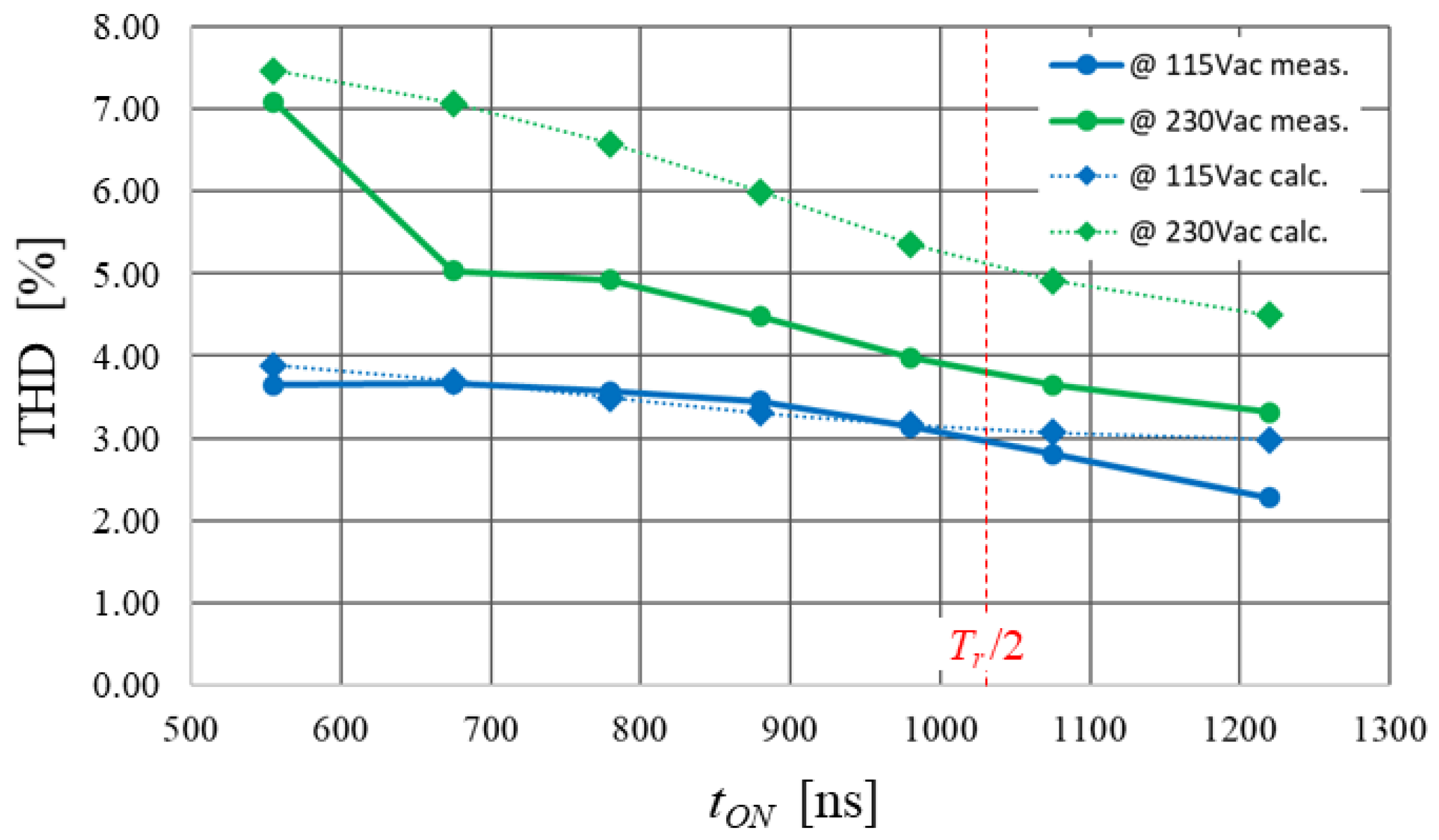
The period of the ringing after demagnetization is 2.07 μs, then Tr/2 = 1.035 μs and the explored range (550 ns to 1.22 μs) includes both conditions tON < Tneg and tON > Tneg for VIN > VR.
Figure 26 shows (round markers connected by solid lines) the measured THD values of the input current
IAC(θ) as a function of different
tON instants, obtained by varying
Cadj, at both 115 Vac and 230 Vac and 100% load. For comparison, the plot shows also the corresponding values obtained by calculation (rhomboid markers connected by dotted lines) reported in the plot of
Figure 13.
The experimental data at low line are very well aligned to those calculated, except for the longest delay where the actual THD trend and the predicted one seem to diverge. At the high line, surprisingly, the measured values are lower than the calculated ones. However, the trend is the same except for the shortest delay, where the two values are much closer to one another. This difference is compatible with a positive offset of the PWM comparator, which increases the positive contribution of the per-cycle charge Qpos and then, tends to reduce the THD.
To complete the experimental analysis, it is worth measuring the impact of tON on converter’s efficiency (h = Pout/Pin). With valley switching (tON = Tr/2 when VIN > VR) the per-cycle energy lost at turn-on is at a minimum and increases as tON moves in either direction. However, with a shorter tON the switching frequency increases slightly (so do capacitive and switching losses) but operation gets closer to transition and the current form factor improves slightly (so conduction losses are a bit lower). With a longer tON there are the opposite changes in power losses. Additionally, a positive initial current causes a small amount of switching losses at turn-on, as if the converter worked in slight CCM.
Figure 27 shows the measured efficiency values of the converter specified in
Table 4 and controlled by the L6562A control IC with the QR method as a function of different
tON instants, the same as those considered in the plot of
Figure 24, at 115 Vac and 230 Vac, 100% and 50% load.
Figure 28 shows the measured efficiency values of the converter specified in
Table 5 and controlled by the HVLED007 control IC with the EQR method as a function of different
tON instants, the same as those considered in the plot of
Figure 26, at 115 Vac and 230 Vac, 100% and 50% load.
In both cases it is possible to observe that the efficiency at low line is essentially insensitive to tON, which is a benign characteristic: since at low line the full load efficiency is at a minimum, i.e., power losses are at a maximum, the thermal design of the converter will be unaffected by the ZCD circuit, its setting, and its tolerances. This makes sense since under these conditions, conduction losses dominate.
At high line, where capacitive and switching losses dominate, the efficiency has a peak in the neighborhood of tON = Tr/2, meaning that capacitive losses are actually dominant. At 50% load this trend becomes more visible at low line as well.
These observations suggest a few system-level design guidelines. In converters controlled with the QR method, since tON has essentially no impact on the THD of the input current, it makes sense to set the ZCD circuit to target tON = Tr/2 to optimize their efficiency. In converters controlled with the EQR method one can aim to minimize the THD of the input current by setting the ZCD circuit to target tON > Tr/2 with no impact on the thermal design. However, by doing so the drop in efficiency at high line and/or lighter load will be more pronounced. This fact should be kept in mind in designs where the electrical specification sets efficiency targets at high line and/or light load as well.
6. Conclusions
Hi-PF QR Flyback is the preferred converter different application thanks to the related high benefit/cost ratio. Although, one can implement an optimal control there are some inherent causes of distortion due to the nonideality of the components. In this work, the distortion due to the actual ZCD circuit has been qualitatively and quantitatively investigated. Moreover, a comparison among three ZCD has been performed. An optimal ZCD circuit does not negatively affect the input current but requires much silicon for implementing the control IC. A differentiator-based ZCD is the worst in terms of THD and, similarly to the previous case, it is silicon consuming. The comparator-plus-delay ZCD circuit enables the best trade-off between performance (only slightly worse than the optimal ZCD circuit) and silicon consumption (the lowest one). Two test benches have been used to experimentally assess the impact of a nonzero current at turn-on on the THD of the input current and verify the aforesaid theoretical predictions, finding a good agreement especially as far as the trend is concerned. The impact of a nonzero current at turn-on on efficiency has been assessed too.
As a conclusion, it is possible to state that the impact of the ZCD circuit on the THD of the input current in Hi-PF QR flyback converters is essentially negligible with the traditional QR method and low with the enhanced QR method. In other words, the detection method, as well as the quality and the performance of the semiconductor components utilized for the ZCD circuit, only slightly affect the THD of the input current or the efficiency of the converter. Therefore, utilizing more sophisticated and/or costly detection circuits does not necessarily provide significant improvement. Rather, it appears that the low-cost comparator-plus-delay ZCD circuit in use in the control ICs considered for the experiments is all in all the best choice.
The experiments have shown also that with the traditional QR method it is possible to set the comparator-plus-delay ZCD circuit to target the maximum conversion efficiency with no impact on the THD of the input current by setting tON = Tr/2. With the enhanced QR method it is possible to have a slight improvement of the THD by setting the ZCD circuit so as to have tON > Tr/2, with no penalty on the thermal design but with a higher deterioration rate of the efficiency at high line and/or light load.


