Sequential Switching Shunt Regulator Parallel Power Processing Control for High Capacitance Solar Arrays


Abstract
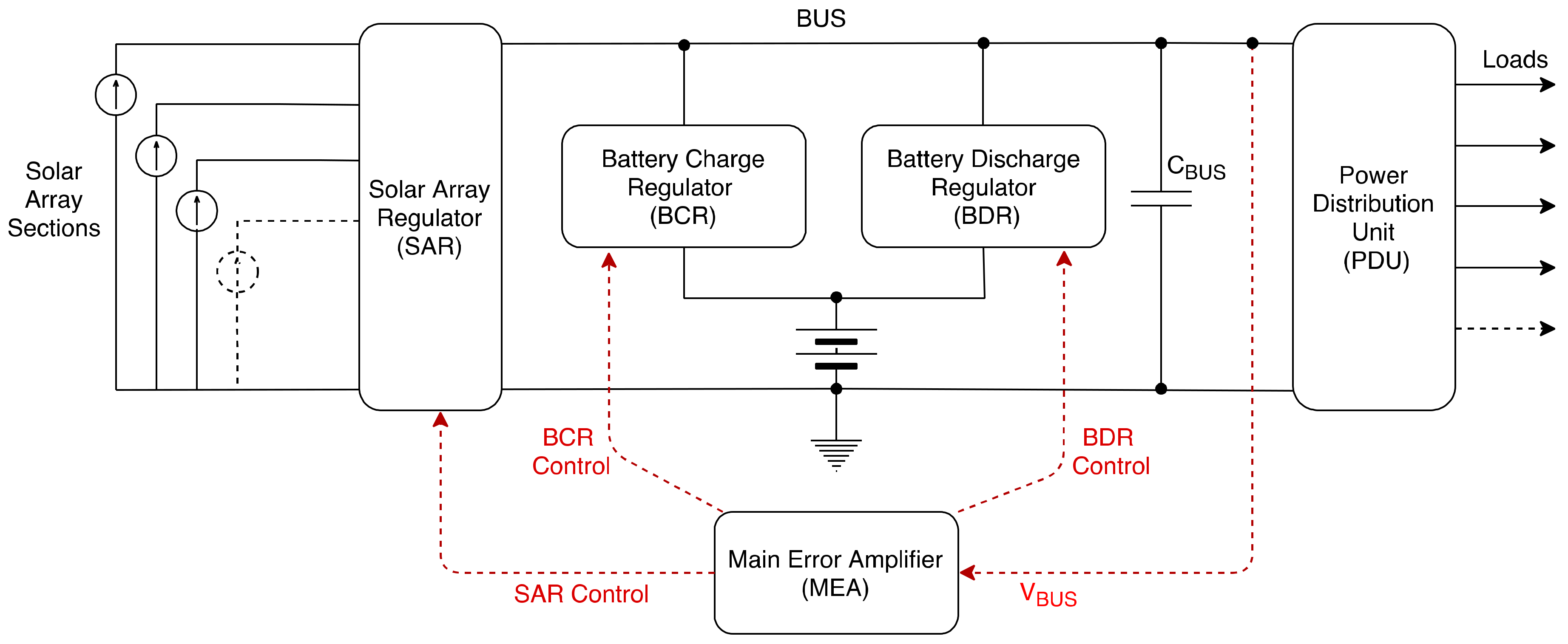
:1. Introduction
- The requirement to use an active current limiter [3,9] to avoid the current spikes produced by the discharge of the CSA at shunt–transistor turn on. When one solar array section is connected to the bus, the CSA is charged to the bus voltage. That energy is dissipated in the shunt transistor when it turns on. The requirement to use an active current limiter has a major drawback because the shunt transistor switching time increases drastically, and this results in an increase of the switching power losses.
- Increase of the dump turn-on delay penalizing the DC characteristic (output voltage ripple) and the AC characteristics (regulator bandwidth and output impedance).
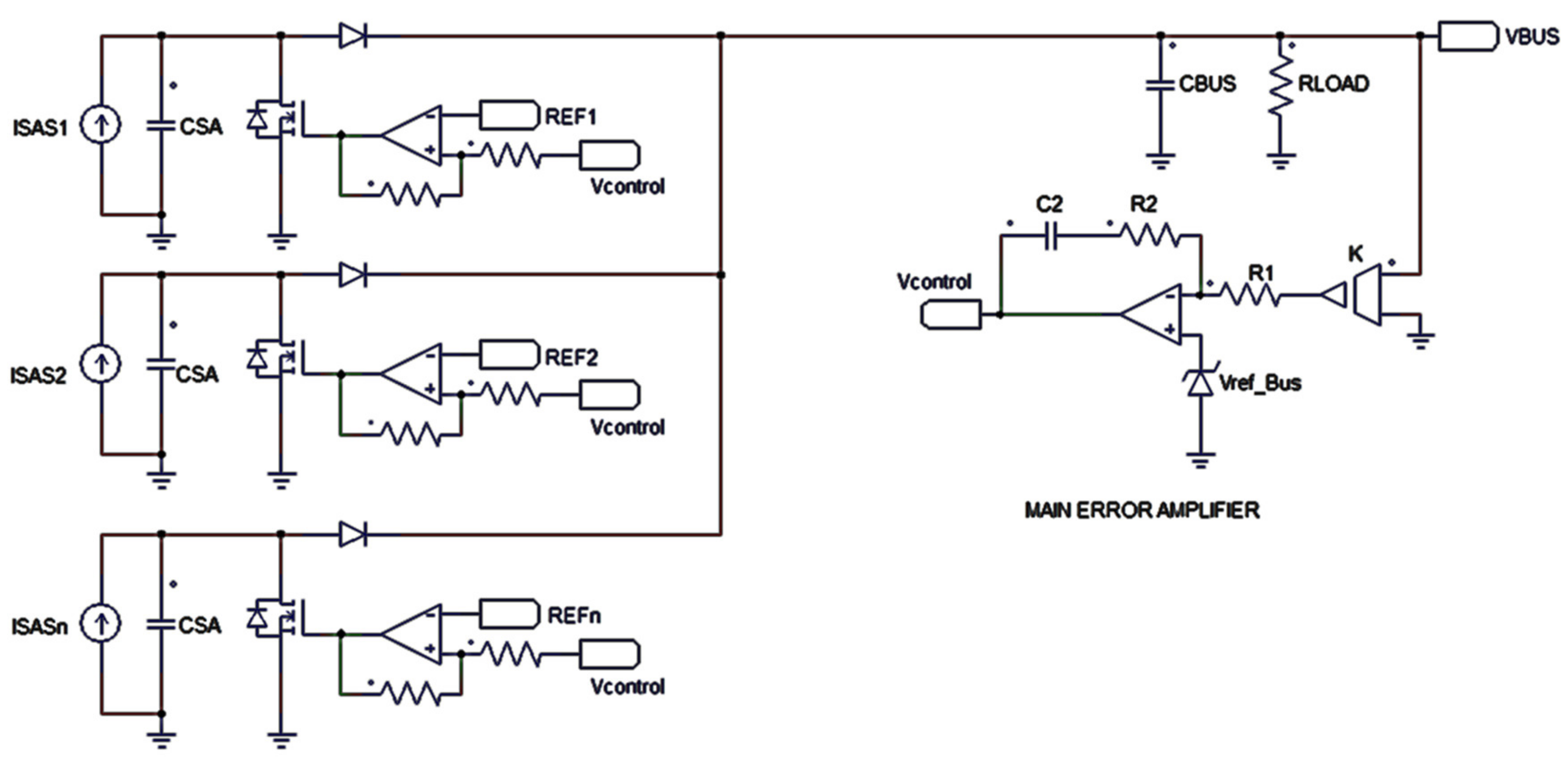
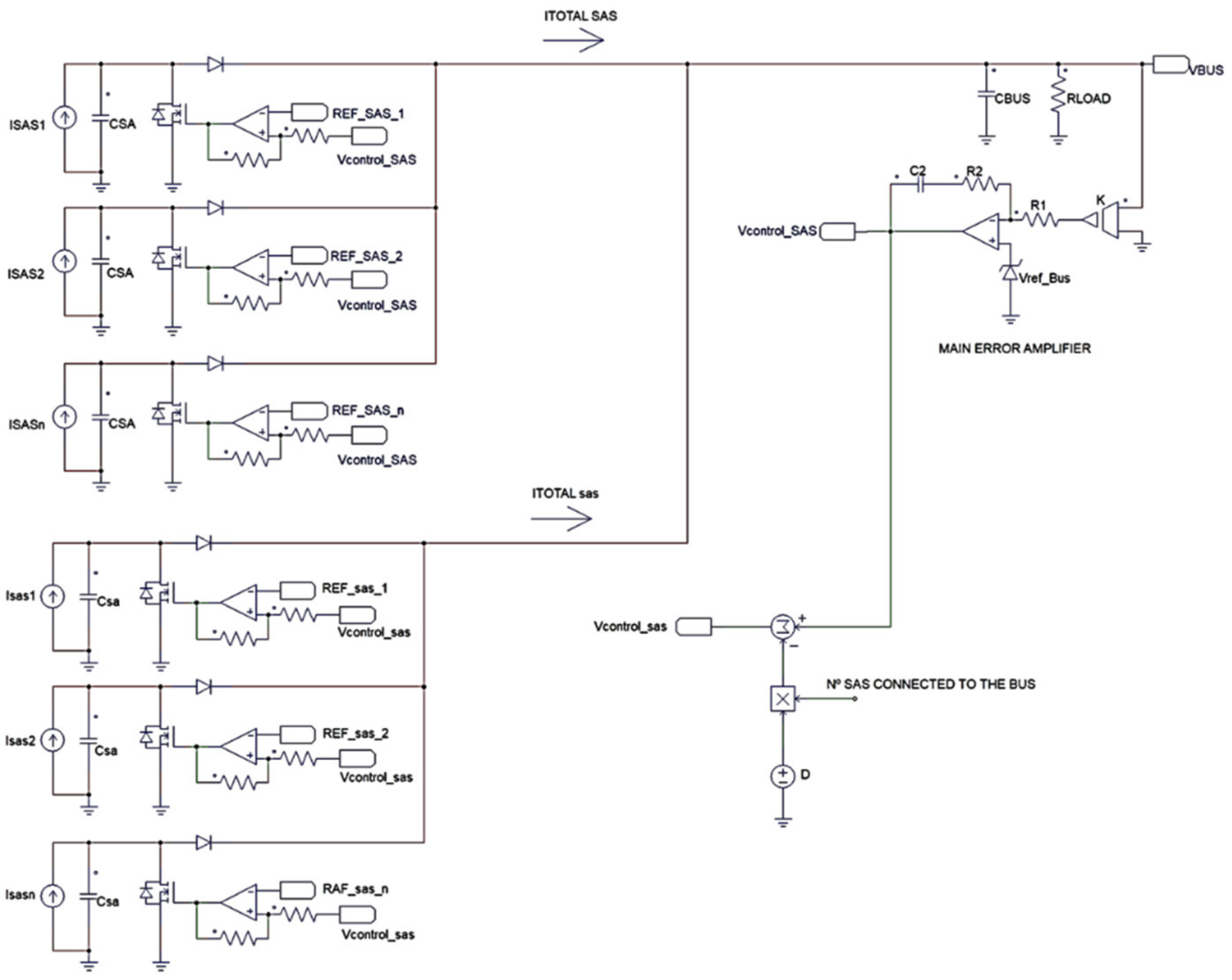
2. Proposed S3R Control Method
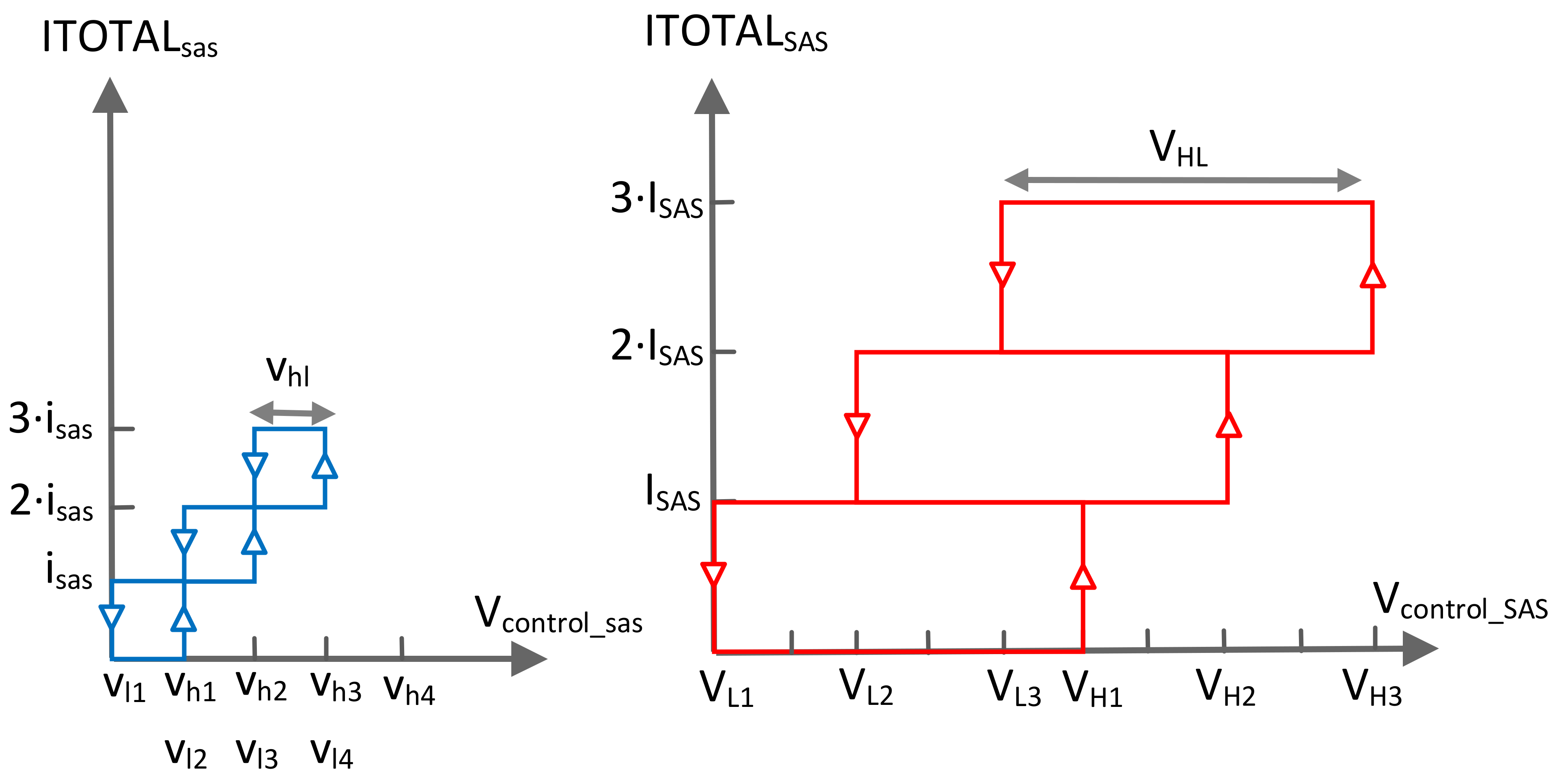
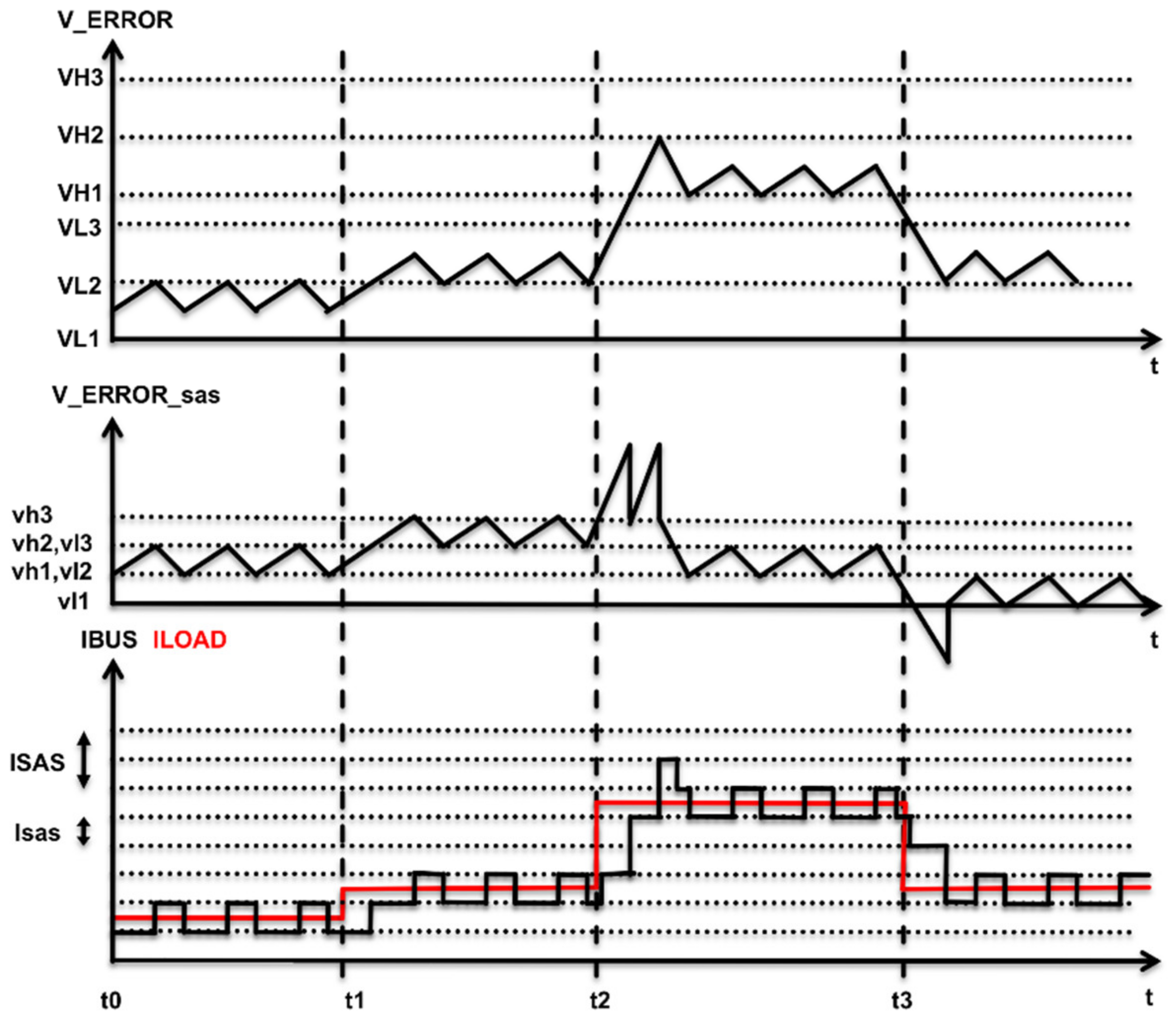
- From t0 to t1 (steady state response): In this state, the low-power Section 2 switches to regulate the bus voltage, while all the high-power sections are fully off. The total load-averaged current is given by Equation (7).ILOAD = Isas1 + <Isas2>
- From t1 to t2 (small load perturbation): At t1, a load current step occurs. VERROR and VERROR_sas increase switching on the upper low-power current sections until the current balance is reached. In this case, the compensation is achieved with the third low-power section. Since the VERROR signal does not cross the VH1 threshold, the high-power sections are not connected. This is the classical S3R response. In this case, the total load-averaged current is given by Equation (8).ILOAD = Isas1 + Isas2 + <Isas3>
- From t2 to t3 (large load perturbation): At t2, a large load current step occurs. Now the low-power sections remaining current is insufficient to compensate the load change. After switching on all the low-power sections, VERROR increases until it crosses the VH1 threshold; at this moment the high-power Section 1 is switched on and a constant voltage is subtracted to VERROR to generate VERROR_sas. The compensation is not yet achieved, so VERROR increases until it crosses the VH2 threshold, at this moment the high-power Section 2 is switched on and the voltage subtracted to VERROR to generate VERROR_sas is doubled, see Equation (9). Now the balance between bus and load currents becomes positive so the control voltage decreases, and the system enters in the small power sections regulation zone. The fine current balance is achieved with the second small power section. The total load-averaged current is given by Equation (10).VERROR_sas = VERROR − 2·DILOAD = Isas1 + <Isas2> + ISAS1 + ISAS2
- From t3 to t4 (large load perturbation): At t3, a large load current step occurs. All the low-power sections are switched off, but this is insufficient to compensate the load change. After switching off all of the low-power sections, VERROR still decreases until it crosses the VL2 threshold; at this moment the high-power Section 2 is switched off and the voltage subtracted to VERROR to generate VERROR_SAS is given by Equation (11). Now the balance between the bus and load currents becomes negative so the control signals increase and the system enters into the small power sections regulation zone. The fine current balance is achieved with the first small power section. The total load-averaged current is given by Equation (12).VERROR_sas = VERROR − DILOAD = <Isas1> + ISAS1
3. Shunt Transistor Turn-On Delay Modeling
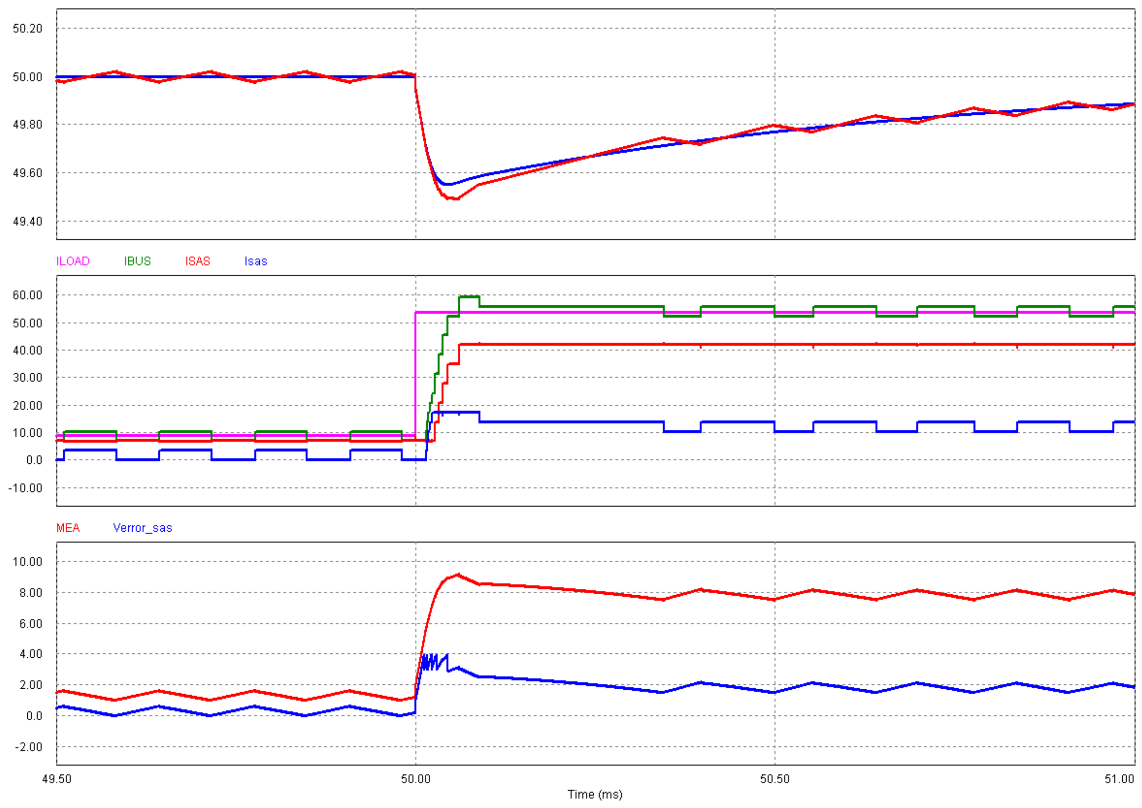
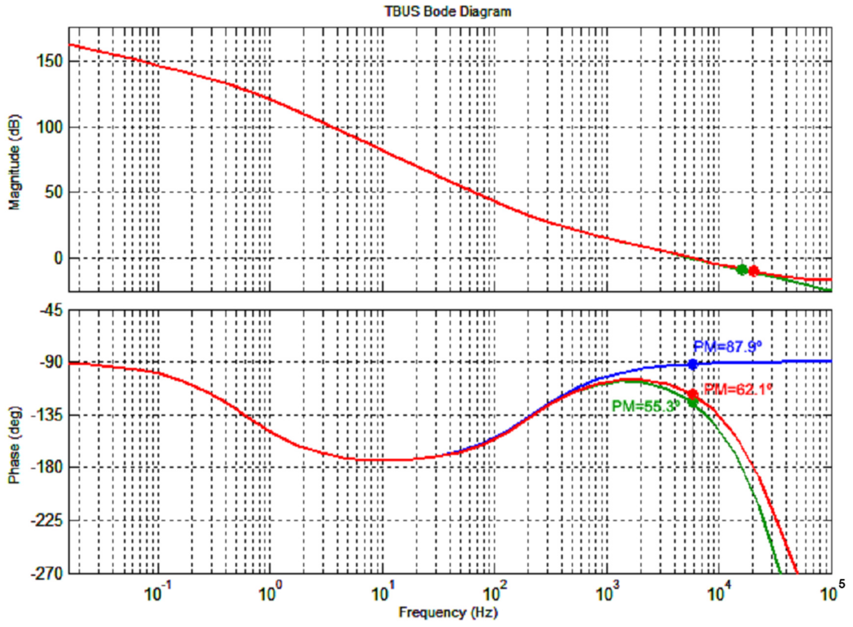
4. Simulation Results
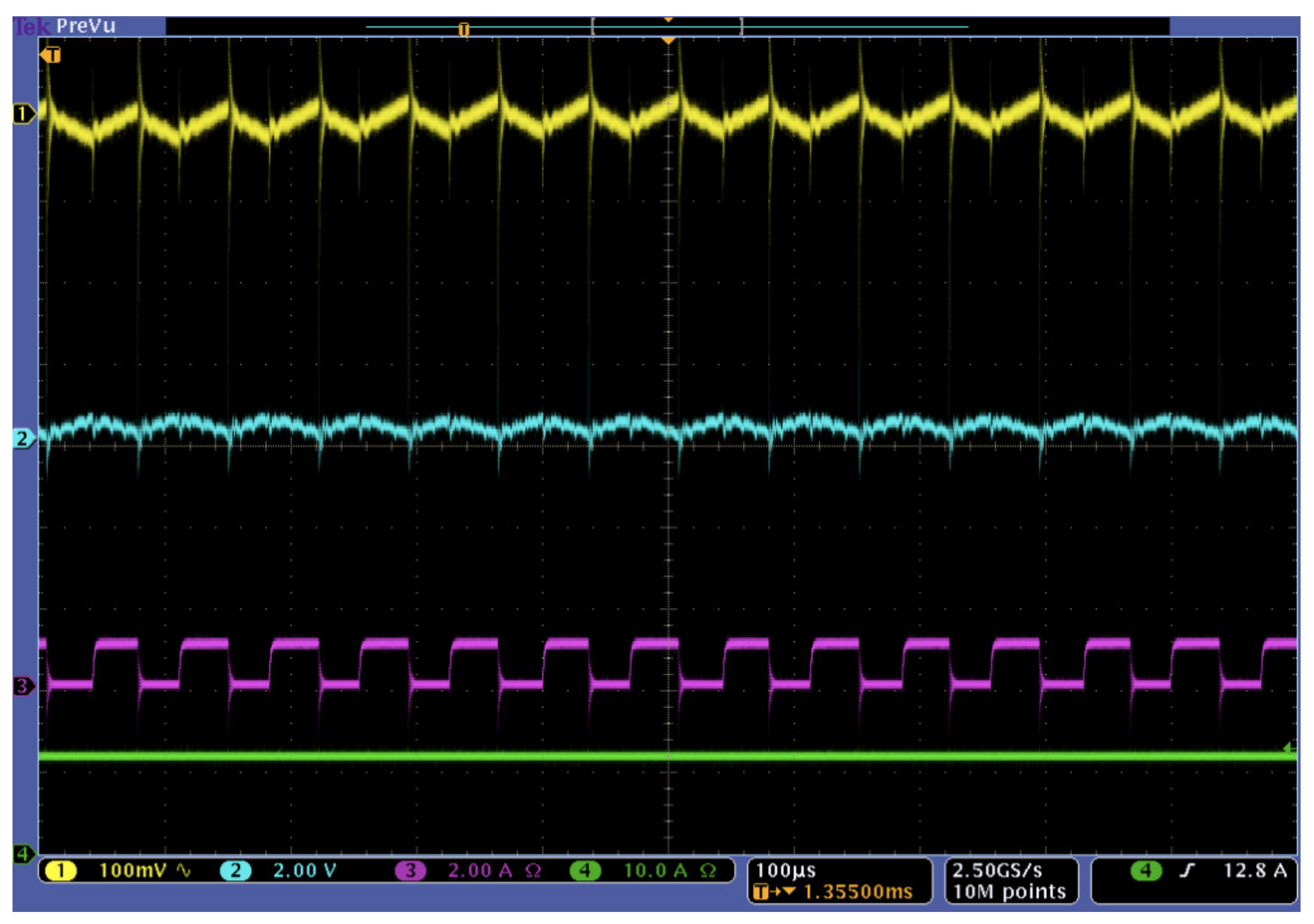
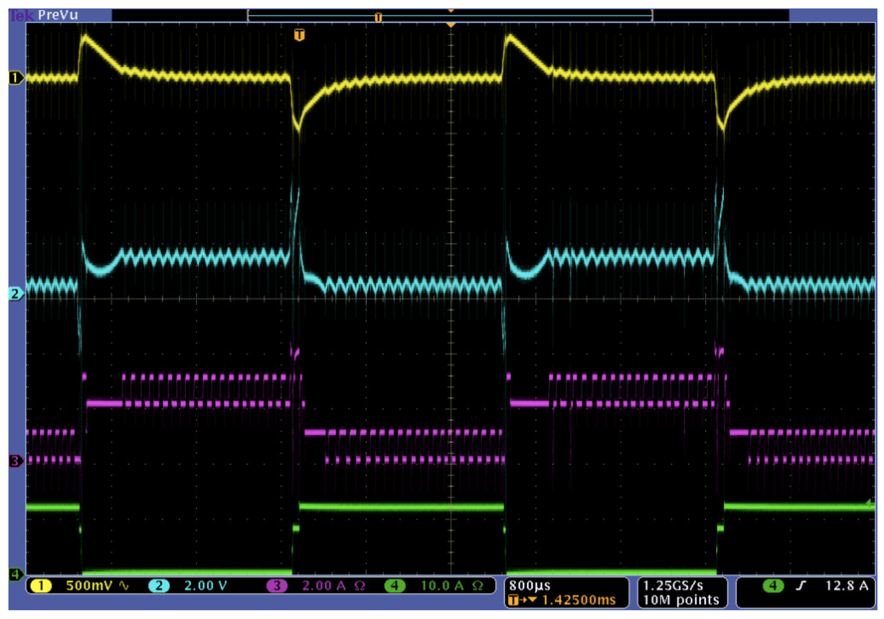
5. Experimental Results
6. Conclusions
Author Contributions
Funding
Institutional Review Board Statement
Informed Consent Statement
Data Availability Statement
Conflicts of Interest
References
- Capel, A.; O’Sullivan, D.; Marpinard, J.C. High-power conditioning for space applications. IEEE Proc. 1998, 76, 391–408. [Google Scholar] [CrossRef]
- O’Sullivan, D.; Weinberg, A.H. The sequential switching shunt regulator (S3R). ESTEC Spacecr. Power Cond. Semin. 1977, ESA SP-126, 123–131. [Google Scholar]
- Zhu, H.; Zhang, D. Design considerations of sequential switching shunt regulator for high-power applications. IEEE Trans. Ind. Electron. 2020, 67, 9358–9369. [Google Scholar] [CrossRef]
- Rueda-Boldó, P.; Fernández-Lisbona, E. Multi Junction Ga/As solar cell capacitance and its impact upon solar arrays regulators. In Proceedings of the Sixth European Space Power Conference, Porto, Portugal, 6–10 May 2002; pp. 29–34. [Google Scholar]
- Blok, R.; van den Berg, E.; Slootweg, D. Solar cell capacitance measurement. In Proceedings of the Sixth European Space Power Conference, Porto, Portugal, 6–10 May 2002; pp. 597–602. [Google Scholar]
- Schwander, D. Dynamic solar cell measurement techniques: New small signal measurement techniques. In Proceedings of the Sixth European Space Power Conference, Porto, Portugal, 6–10 May 2002; pp. 603–608. [Google Scholar]
- Barde, H. Comparison of three different methods for the characterisation of triple junction GaAs space solar cells. In Proceedings of the Seventh European Space Power Conference, Stresa, Italy, 9–13 May 2005; pp. 91–97. [Google Scholar]
- Garrigós, A.; Blanes, J.M.; Carrasco, J.A.; Ejea, J.B. Influence of the parasitic solar array capacitance in the Sequential Switching Shunt Series Regulator. In Proceedings of the 13th IEEE Mediterranean Electrotechnical Conference, Malaga, Spain, 16–19 May 2006; pp. 1198–1201. [Google Scholar]
- Delepaut, C.; Martin, M. Current limitation techniques in a S3R power cell. In Proceedings of the Third European Space Conference, Graz, Austria, 23–27 August 1993; pp. 61–66. [Google Scholar]
- Ebale, G.; Lamantia, A.; La Bella, M. Power Control System for the AGILE Satellite. In Proceedings of the Seventh European Space Power Conference, Stresa, Italy, 9–13 May 2005; pp. 589–596. [Google Scholar]
- Garrigós, A.; Carrasco, J.A.; Blanes, J.M.; Sanchis-Kilders, E. A new Sequential Swithching Shunt Regulator –Digital Shunt Regulator (S3R-DSR) for solar array regulators. In Proceedings of the IEEE International Symposium on Industrial Electronics, Montreal, QC, Canada, 9–13 July 2006; pp. 1064–1069. [Google Scholar]
- Fernández, A.; González, J.R. Modelling of the section capacitance to interfere with a S3R. In Proceedings of the Eleventh European Space Power Conference, Thessaloniki, Greece, 3–7 October 2016. [Google Scholar]
- O’Sullivan, D.; Spruyt, H.; Crausaz, A. PWM conductance control. In Proceedings of the19th Annual IEEE Power Electronics Specialists Conference, Kyoto, Japan, 11–14 April 1988; pp. 351–359. [Google Scholar]
- Capel, A.; Perol, P. Comparative performance evaluation between the S4R and the S3R regulated bus topologies. In Proceedings of the IEEE Annual Power Electronics Specialists Conference, Vancouver, BC, Canada, 17–21 June 2001; pp. 1963–1969. [Google Scholar]


| System Specifications | |
|---|---|
| Power | 4500 W |
| Csa | 0.3 μF/A |
| Bus voltage (VBUS) | 50 V |
| Bus voltage ripple (ΔVBUS) | <1% VBUS |
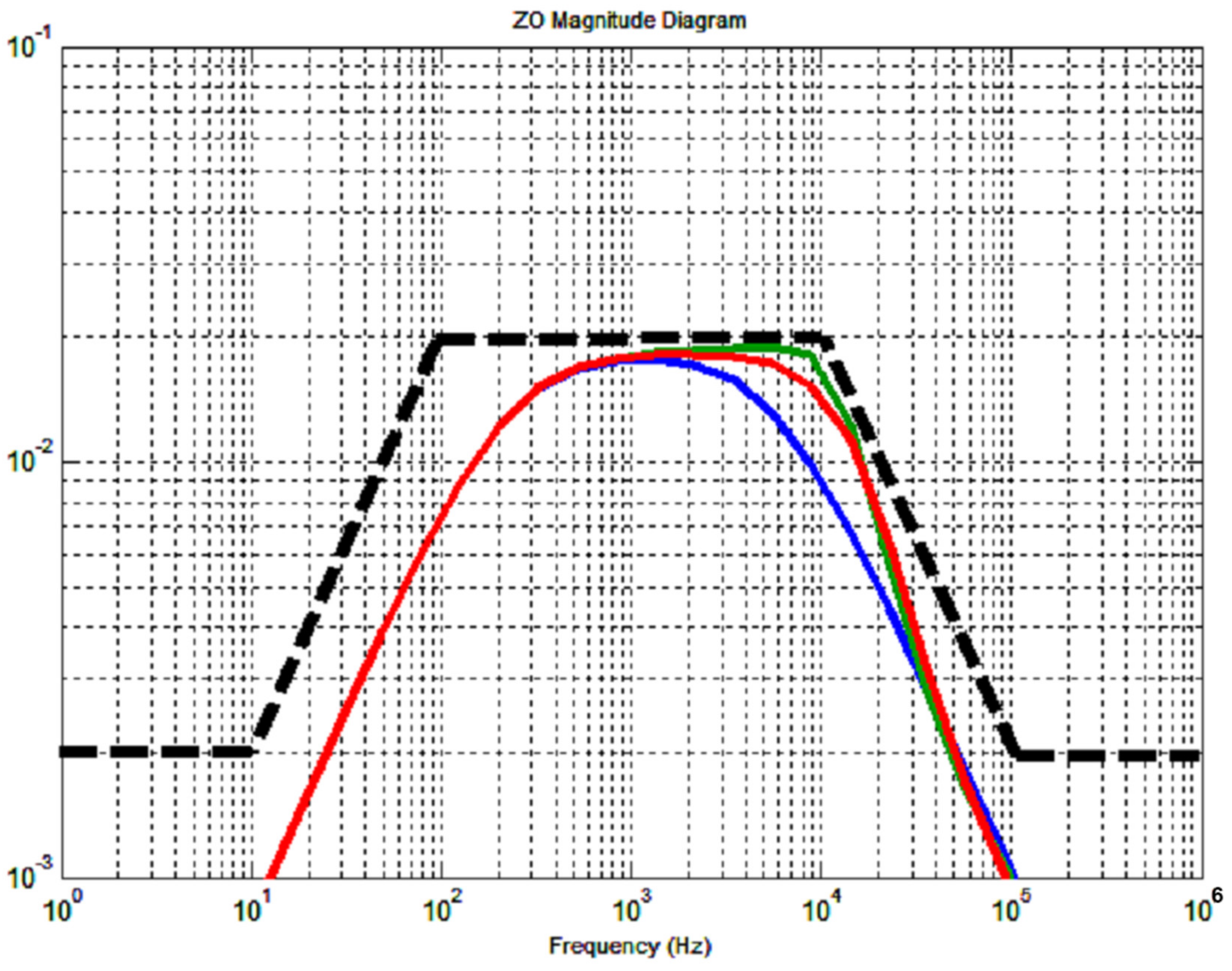
| Maximum output impedance (ZO max) | 11.1 mΩ |
| Control loop gain margin | ≥10 dB |
| Control loop phase margin | ≥60° |
| System Specifications | |
|---|---|
| Number of high-power solar array sections (SAS) | 10 (7 A/section) |
| Number of low-power solar array sections (sas) | 6 (3.5 A/section) |
| Bus capacitance | 2.76 mF |
| G | 7 A/V |
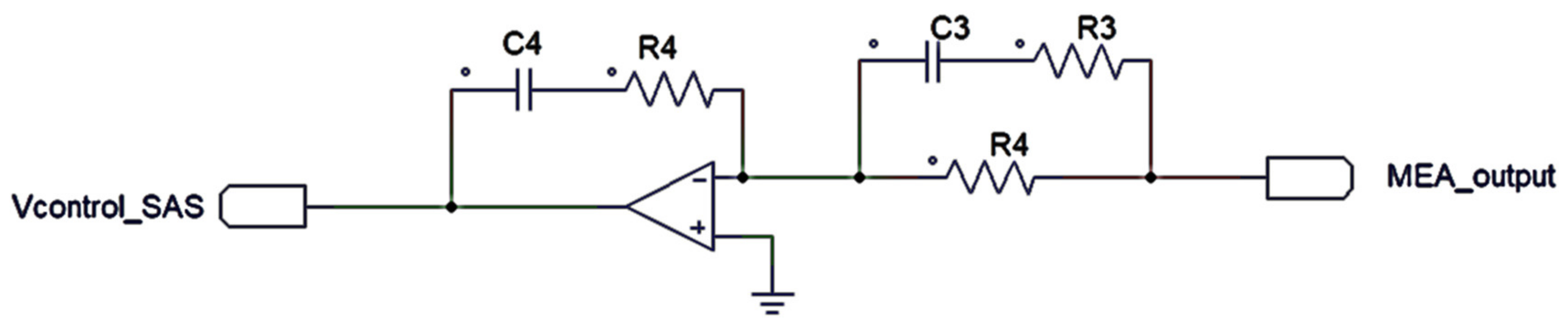
| K | 0.1 |
| R1 | 1 kΩ |
| R2 | 145 kΩ |
| C2 | 5 nF |
| R3 | 100 Ω |
| C3 | 3.7 nF |
| R4 | 1 kΩ |
| C4 | 3 pF |
| Breadboard System Specifications | |
|---|---|
| Power | 1200 W |
| Bus voltage (VBUS) | 50 V |
| Bus voltage ripple (ΔVBUS) | <1% VBUS |
| Maximum output impedance (ZO max) | 50 mΩ |
| Control loop gain margin | ≥10 dB |
| Control loop phase margin | ≥60° |
| High-power solar array sections | 3 (4 A/section) |
| Low-power solar array sections | 4 (1 A/Section) |
| Bus capacitance | 480 μF |
Publisher’s Note: MDPI stays neutral with regard to jurisdictional claims in published maps and institutional affiliations. |
© 2021 by the authors. Licensee MDPI, Basel, Switzerland. This article is an open access article distributed under the terms and conditions of the Creative Commons Attribution (CC BY) license (http://creativecommons.org/licenses/by/4.0/).
Share and Cite
Blanes, J.M.; Carrasco, J.A.; Garrigós, A.; Marroquí, D.; Torres, C. Sequential Switching Shunt Regulator Parallel Power Processing Control for High Capacitance Solar Arrays. Energies 2021, 14, 429. https://doi.org/10.3390/en14020429
Blanes JM, Carrasco JA, Garrigós A, Marroquí D, Torres C. Sequential Switching Shunt Regulator Parallel Power Processing Control for High Capacitance Solar Arrays. Energies. 2021; 14(2):429. https://doi.org/10.3390/en14020429
Chicago/Turabian StyleBlanes, José M., José A. Carrasco, Ausiàs Garrigós, David Marroquí, and Cristian Torres. 2021. "Sequential Switching Shunt Regulator Parallel Power Processing Control for High Capacitance Solar Arrays" Energies 14, no. 2: 429. https://doi.org/10.3390/en14020429