
A PI + Sliding-Mode Controller Based on the Discontinuous Conduction Mode for an Unidirectional Buck–Boost Converter with Electric Vehicle Applications

 ,
,  , , and
Abstract
:1. Introduction
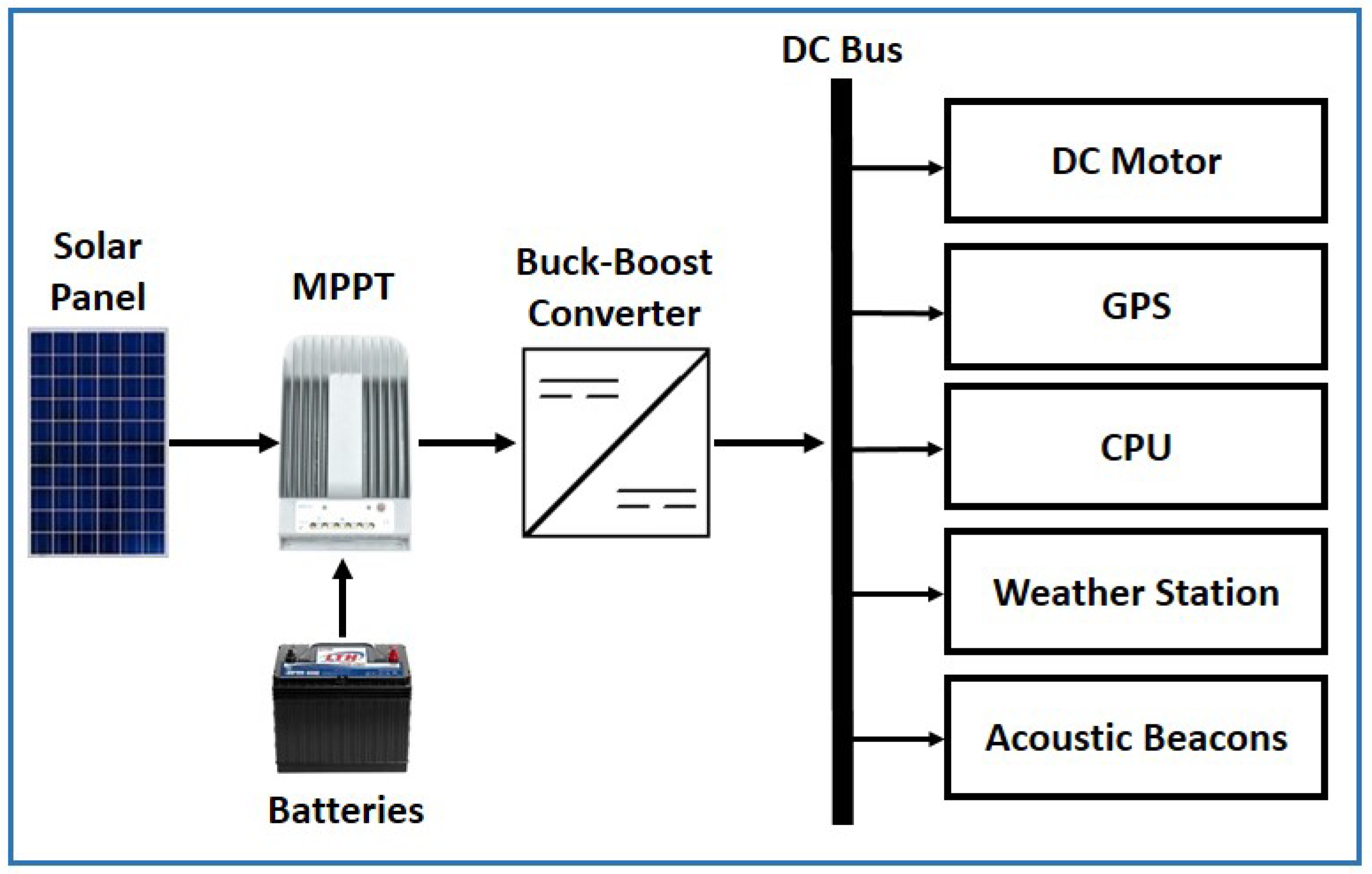
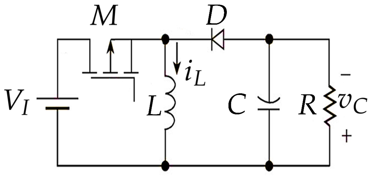
2. Buck–Boost Converter Modeling and Physical Considerations in DCM
Auxiliary Signal Determination
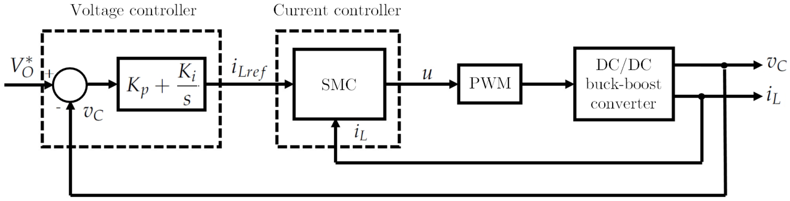
3. Controller Design for Output Voltage Regulation
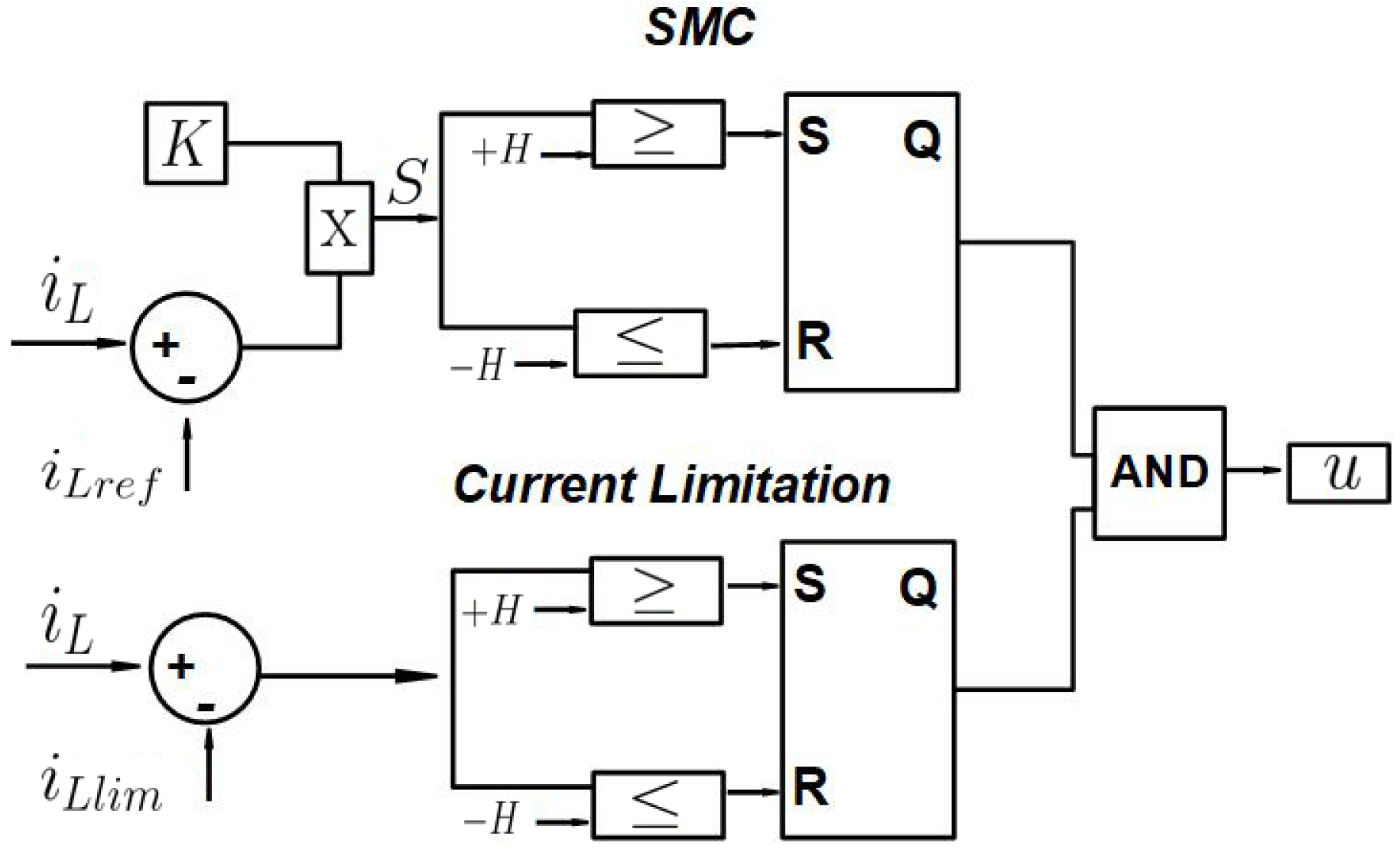
3.1. Sliding-Mode Current Controller
3.1.1. Sliding Surface Selection
3.1.2. Equivalent Control
3.1.3. Lyapunov Stability Analysis
3.1.4. Hysteresis Function
3.2. Proportional–Integral Voltage Controller
4. Numerical Results and Discussion
4.1. Simulation Scenario I: Converter Open-Loop Behavior
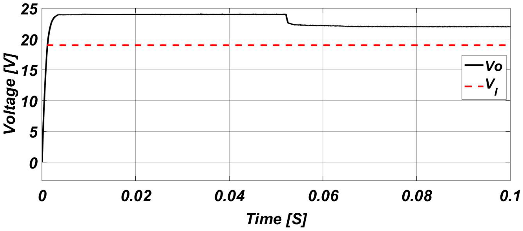
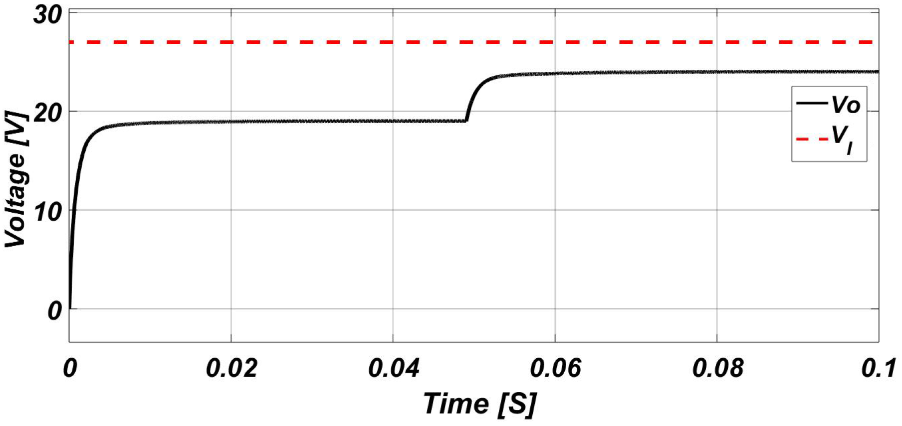
4.2. Simulation Scenario II: Input Voltage Variations
4.3. Simulation Scenario III: Resistance Load Variations
4.4. Simulation Scenario IV: Output Voltage Reference Variations
5. Conclusions and Future Work
Author Contributions
Funding
Institutional Review Board Statement
Informed Consent Statement
Data Availability Statement
Conflicts of Interest
References
- Teoh, Y.H.; Huspi, H.A.; How, H.G.; Sher, F.; Din, Z.U.; Le, T.D.; Nguyen, H.T. Effect of Intake Air Temperature and Premixed Ratio on Combustion and Exhaust Emissions in a Partial HCCI-DI Diesel Engine. Sustainability 2021, 13, 8593. [Google Scholar] [CrossRef]
- Khzouz, M.; Gkanas, E.I.; Shao, J.; Sher, F.; Beherskyi, D.; El-Kharouf, A.; Al Qubeissi, M. Life Cycle Costing Analysis: Tools and Applications for Determining Hydrogen Production Cost for Fuel Cell Vehicle Technology. Energies 2020, 13, 3783. [Google Scholar] [CrossRef]
- Park, D.R.; Kim, Y. Design and Implementation of Improved High Step-Down DC-DC Converter for Electric Vehicles. Energies 2021, 14, 4206. [Google Scholar] [CrossRef]
- Zhang, Z.; Zhou, D.; Xiong, N.; Zhu, Q. Non-Fragile H∞ Nonlinear Observer for State of Charge Estimation of Lithium-Ion Battery Based on a Fractional-Order Model. Energies 2021, 14, 4771. [Google Scholar] [CrossRef]
- B, A.R.; Vuddanti, S.; Salkuti, S.R. Review of Energy Management System Approaches in Microgrids. Energies 2021, 14, 5459. [Google Scholar] [CrossRef]
- Hart, D.W. Power Electronics; McGraw-Hill: New York, NY, USA, 2001; pp. 217–222. [Google Scholar]
- Chen, Z. Double loop control of buck-boost converters for wide range of load resistance and reference voltage. IET Control Theory Appl. 2012, 6, 900–910. [Google Scholar] [CrossRef]
- Alawieh, A. Hybrid and Nonlinear Control of Power Converters. Ph.D. Dissertation, Université Paris-SUD, Paris, France, 2013. [Google Scholar]
- Chong Tan, S.; Ming Lai, Y.; Kong Tse, C. Sliding Mode Control of Switching Power Converters: Techniques and Implementation; Taylor & Francis Group: London, UK; New York, NY, USA, 2012; pp. 35–51. [Google Scholar]
- O´Dweyer, A. Handbook of PI and PID Controller Tuning Rules, 3rd ed.; Imperial College Press: London, UK, 2009; pp. 1–16. [Google Scholar]
- Tan, S.C.; Lai, Y.M.; Tse, C.K.; Martinez-Salamero, L. Special family of PWM-based sliding-mode voltage controlllers for basic DC-DC converters in discontinuos conduction mode. IET Electr. Power Appl. 2007, 1, 64–74. [Google Scholar] [CrossRef] [Green Version]
- Tan, S.C.; Lai, Y.M.; Tse, C.K.; Cheung, M.K. Adaptive feedforward and feedback control schemes for sliding mode controlled power converters. IEEE Trans. Power Electron. 2006, 21, 182–192. [Google Scholar] [CrossRef]
- Guldemir, H. Modeling and Sliding Mode Control of DC-DC Buck-Boost Converter. In Proceedings of the 6th International Advanced Technologies Symposium (IATS’11), Elazığ, Turkey, 16–18 May 2011; pp. 475–480. [Google Scholar]
- Salimi, M.; Soltani, J.; Markadeh, G.A.; Abjadi, N.R. Indirect output voltage regulation of DC-DC buck/boost converter operating in continuous and discontinuous conduction modes using adaptive backstepping approach. IET Power Electron. 2013, 6, 732–741. [Google Scholar] [CrossRef] [Green Version]
- Salimi, M.; Hajbani, V. Sliding-mode control of the DC-DC flyback converter in discontinuous conduction mode. In Proceedings of the 6th Annual International Power Electronics, Drive Systems, and Technologies Conference, PEDSTC 2015, Tehran, Iran, 3–4 February 2015; pp. 13–18. [Google Scholar] [CrossRef]
- Hu, J.; He, H.; Wei, Z.; Li, Y. Disturbance-Immune and Aging-Robust Internal Short Circuit Diagnostic for Lithium-Ion Battery. IEEE Trans. Ind. Electron. 2021, 1. [Google Scholar] [CrossRef]
- Wei, Z.; Hu, J.; He, H.; Li, Y.; Xiong, B. Load Current and State-of-Charge Coestimation for Current Sensor-Free Lithium-Ion Battery. IEEE Trans. Power Electron. 2021, 36, 10970–10975. [Google Scholar] [CrossRef]
- Li, Y.; Wei, Z.; Xiong, B.; Vilathgamuwa, D.M. Adaptive Ensemble-Based Electrochemical-Thermal-Degradation State Estimation of Lithium-Ion Batteries. IEEE Trans. Ind. Electron. 2021, 1. [Google Scholar] [CrossRef]
- Fadil, H.; Giri, F.; Haloua, M.; Ouadi, H.; Chaoui, F. Nonlinear and adaptive control of buck-boost power converters. LAPISMRA 2002 1996, 11, 578–584. [Google Scholar]
- Kazimierczuk, M.K. Pulse-Width Modulated DC–DC Power Converters; John Wiley & Sons, Ltd.: Dayton, OH, USA, 2008; pp. 139–174. [Google Scholar]
- Diaz-Saldierna, L.; Leyva-Ramos, J.; Langarica-Cordoba, D.; Ortiz-Lopez, M. Energy processing from fuel-cell systems using a high-gain power dc-dc converter: Analysis, design, and implementation. Int. J. Hydrogen Energy 2021, 46, 25264–25276. [Google Scholar] [CrossRef]
- Sira-Ramirez, H.J.; Ilic, M. A Geometric Approach to the Feedback Control of Switch Mode DC-to-DC Power Supplies. IEEE Trans. Circuits Syst. 1998, 35, 1291–1298. [Google Scholar] [CrossRef]
- González Valencia, M. Control de Convertidores Conmutados CC-CC Basado en Modos Deslizantes. Master’s Thesis, Universidad Tecnólogica de Pereira, Risaralda, Colombia, 2017. [Google Scholar]
- Calvente Calvo, F.J. Control en Modo Deslizante Aplicado a Sistemas de Acondicionamiento de Potencia de Satélites. Ph.D. Dissertation, Universidad Politécnica de Cataluña, Barcelona, Spain, 2002. [Google Scholar]
- Utkin, V. Sliding mode control of DC/DC converters. J. Frankl. Inst. 2013, 2146–2165. [Google Scholar] [CrossRef] [Green Version]
- Calvente, J.; Ramirez-Murillo, H.; Vidal-Idiarte, E.; Giral, R.; Restrepo, C. Multisampled average current control of switching power converters. In Proceedings of the 2015 IEEE International Conference on Industrial Technology (ICIT), Seville, Spain, 17–19 March 2015; Volume 15, pp. 2120–2124. [Google Scholar] [CrossRef]
- Ang, S.S.; Dekker, M. Power-Switching Converters; CRC Press: New York, NY, USA, 1995. [Google Scholar]


| Device | Model | No. | Imin (A) | Imax (A) |
|---|---|---|---|---|
| DC Motor | Xi5 Saltwater | 2 | 2 | 12.6 |
| GPS | Trimble BX992 | 1 | 0.5 | 4 |
| CPU | LIVA | 1 | 1 | 3 |
| Weather Station | Airmar 220WX | 1 | 0.05 | 0.09 |
| Acoustic Beacons | Sea Trac X150 | 1 | 0.05 | 0.8 |
| Total: | 3.6 | 20 | ||
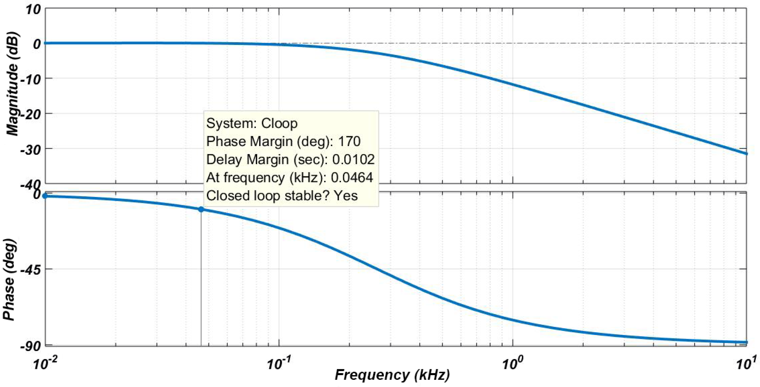
| Controller Gains | ||
|---|---|---|
| (ms) | ||
| 7.56 | 1.45 | 192 |
| Description | Parameter | Value |
|---|---|---|
| Min input voltage | 19 V | |
| Max input voltage | 27 V | |
| Capacitance | C | 1.10 mF |
| Inductance | L | 20 H |
| Inductor resistance | ESR | 1.21 m |
| Switching frequency | f | 20 kHz |
| Min load resistance | R | 1.2 |
| Max load resistance | R | 6.67 |
| Desired output voltage | 24 V |
Publisher’s Note: MDPI stays neutral with regard to jurisdictional claims in published maps and institutional affiliations. |
© 2021 by the authors. Licensee MDPI, Basel, Switzerland. This article is an open access article distributed under the terms and conditions of the Creative Commons Attribution (CC BY) license (https://creativecommons.org/licenses/by/4.0/).
Share and Cite
González, I.; Sánchez-Squella, A.; Langarica-Cordoba, D.; Yanine-Misleh, F.; Ramirez, V. A PI + Sliding-Mode Controller Based on the Discontinuous Conduction Mode for an Unidirectional Buck–Boost Converter with Electric Vehicle Applications. Energies 2021, 14, 6785. https://doi.org/10.3390/en14206785
González I, Sánchez-Squella A, Langarica-Cordoba D, Yanine-Misleh F, Ramirez V. A PI + Sliding-Mode Controller Based on the Discontinuous Conduction Mode for an Unidirectional Buck–Boost Converter with Electric Vehicle Applications. Energies. 2021; 14(20):6785. https://doi.org/10.3390/en14206785
Chicago/Turabian StyleGonzález, Ileana, Antonio Sánchez-Squella, Diego Langarica-Cordoba, Fernando Yanine-Misleh, and Victor Ramirez. 2021. "A PI + Sliding-Mode Controller Based on the Discontinuous Conduction Mode for an Unidirectional Buck–Boost Converter with Electric Vehicle Applications" Energies 14, no. 20: 6785. https://doi.org/10.3390/en14206785