Abstract
This work presents a comprehensive theoretical analysis of current-mode power amplifiers as a function of input power for different biasing classes under the common simplifying assumption of constant transconductance and hard current cut-off/saturation. Typically, the theoretical analysis of power amplifier performance and behavior are carried out only at maximum output power. However, to achieve high data-rates, modern telecommunication systems adopt signals characterized by a very high peak-to-average power ratio, thus it is useful to analyze the power amplifier behavior as a function of power back-off. Moreover, in many cases, to enhance the efficiency and/or to apply harmonic shaping techniques, a clipped drain-source current, which approaches a square wave, is required. The classical analysis can be extended to low power levels only under the assumption of power-independent conduction angle, which is true only for class-A and class-B amplifiers, and does not take into account possible waveform clipping at maximum current. This work presents a complete theoretical Fourier analysis of FET-based power amplifiers as a function of quiescent drain-source current at any input power level and accounting for the clipped current case, up to the square-wave limit, reorganizing and completing the material that can be found in classical textbooks in the field.
1. Introduction
High-frequency power amplifiers (PAs), from RF to microwave and millimeter-wave range, are key elements of any wireless system. Output power capability/density is the essential feature of a PA, but, beyond this, the PA must also be highly efficient, being one of the most power-hungry elements of a transceiver, show reasonable gain, to avoid long amplifying chains, and keep a predefined level of linearity, to preserve information [1]. PA design is always made challenging by non-idealities, such as device parasitic reactances, strongly limiting achievable bandwidths, electro-magnetic crosstalk and/or thermal issues, which all become increasingly critical at higher frequencies. This implies that practical design must rely as much as possible on fully nonlinear device models, accounting for most possible parasitic and high-order nonlinear effects: an approach that has been made possible only by Computer-Aided Design (CAD). At the time where CAD tools were not available, a big effort was put by research in the microwave field to investigate and develop novel PA architectures based on simplified mathematical device models that allow a fully analytical analysis though Fourier expansion of the involved signals [2,3,4,5]. However, theoretical PA analysis is presently still fundamental to acquire a deep understanding of the working principle standing behind the different PA architectures which is the basis of any practical design. Moreover, it is extremely useful to rapidly estimate achievable performance from basic physical device parameters (maximum current, threshold voltage, etc.) without the need for time-consuming nonlinear CAD simulations and optimizations. PA design based upon voltage and current waveform limits, i.e., considering only waveform clipping as the essential nonlinearity of the circuit, is called load-line design approach [6,7,8,9] and it represents a fundamental tool for the initial design phase consisting of device sizing, topology selection and first-round optimization, as it gives approximate but yet trustable results in much less time compared to fully nonlinear simulations. Then, according to the selected technology and operating frequency, secondary nonlinear effects can be more or less pronounced and hence require more or less nonlinear optimizations/simulations. Experience, however, suggests that theoretical predictions and final results are never far off [2,6,10,11].
Once the harmonic components of the (possibly clipped) current and voltage waveforms are known, the design rules for the PA terminations can be derived, according to the specific design target [12,13,14]. In other words, Fourier analysis [2,5] can be exploited for the theoretical analysis of any kind of PA architecture, from classical current-mode tuned-load (TL) PAs [11] to advanced architectures based on waveform engineering [15], like the harmonic tuned PA [16,17,18], the class-J PA [19,20], the class-FPA [21,22], and their variants [23,24,25,26], on switched device operation, such as class-E [27], on series-power combination (stacked PA) [28,29,30], or finally on the load [31] and supply modulation [32] concepts.
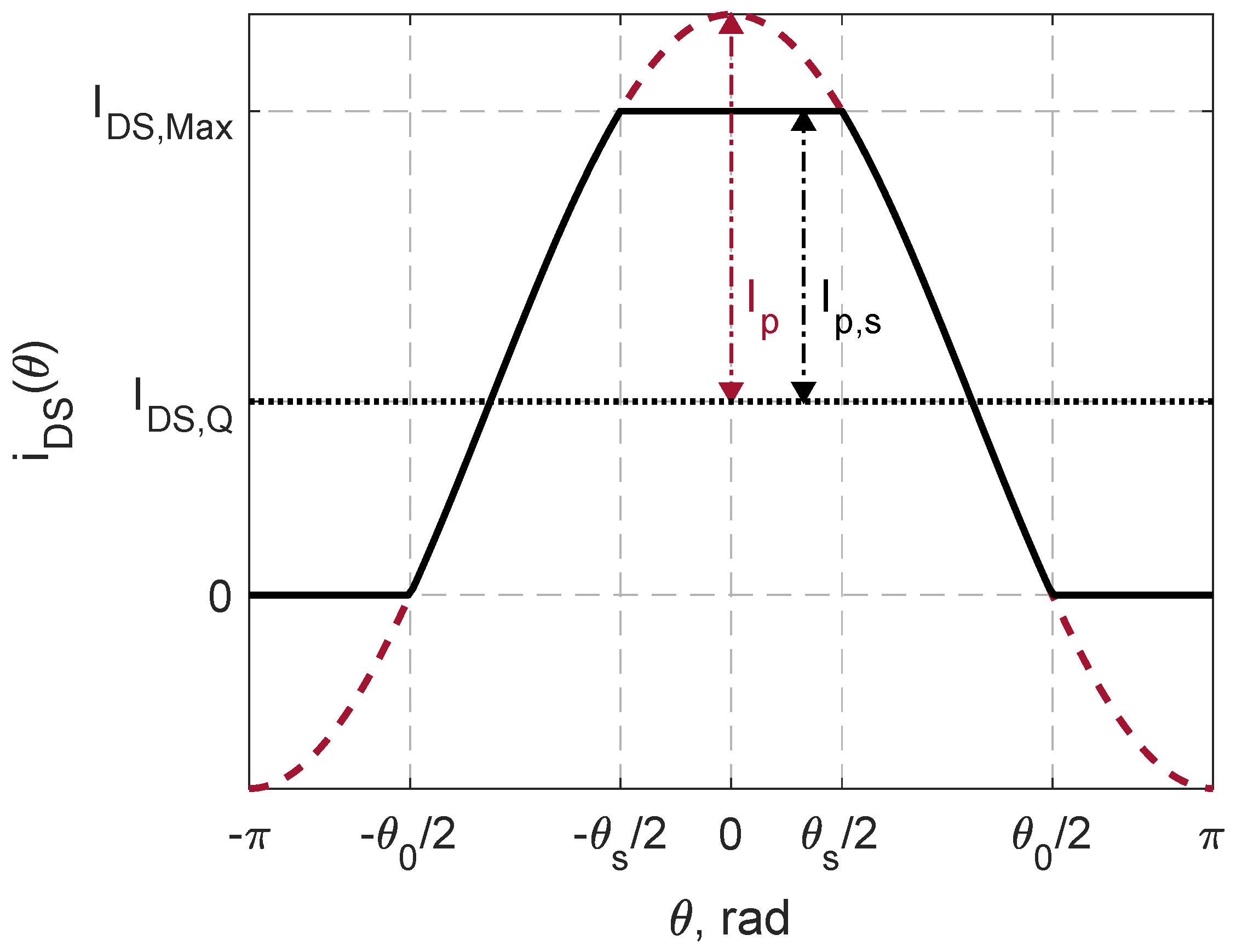
Many microwave circuit textbooks [7,9,13,33] report PA harmonic analysis, but the latter is typically limited to the case of a PA operated at the limit linear behavior (linear if a class-A PA is considered, otherwise the current waveform is already distorted by clipping due to pinch-off.), considered, in the simplified load-line approach, as the maximum output power. To enhance performance, modern telecommunication systems adopt signals characterized by high peak-to-average power ratios (PAPRs), which makes essential to extend harmonic analysis to any level of power back-off. Moreover, efficiency-enhancement and waveform engineering techniques often require waveform “squaring”, which implies an extension of the analysis to the case of current waveforms that are clipped both toward low and high values, as shown in Figure 1.

Figure 1.
Clipped drain-source current waveform.
Aim of this work is to provide a more comprehensive and well-ordered mathematical formulation of the classical harmonic analysis of FET-based current-mode power amplifiers, under the classical assumption of constant transconductance, collecting, reorganizing and upgrading the material that can be found in several textbooks, e.g., [9,12,13,33]. The analysis is generalized to any biasing class and input power level and extended to the case of waveform clipping at maximum current, treated as an equivalent input over-driving, by resorting to a simple formalism based on two parameters: , depending only on the selected bias point and , related instead to the input back-off or to the (equivalent) input over-driving.
The rest of the paper is organized as follows: Section 2 describes the simplified device model adopted for the analysis, recalls the fundamental definitions of operating and biasing classes and introduces the basic parameters adopted for the subsequent Fourier coefficient calculations, detailed in Section 3 and in the Appendices. Finally, Section 4 demonstrates the application of the proposed Fourier formalism to the analysis of the tuned-load PA [3], while Section 5 concludes the work with a summary.
2. Drain-Source Current Model
Active semiconductor device modeling is a vast subject [34]. Physics-based/TCAD models and black-box/behavioral models [35,36,37,38] may be adopted in CAD to gain, respectively, accuracy or computational efficiency, but are not usable for theoretical analysis, which requires instead an equivalent-circuit model. Such models are conceived relying on physical consideration and then fitted on device measurements to better represent a specific technology. Device physics suggests that circuit models can separately model parasitics and intrinsic resistive and reactive effects with proper passive elements [33], and current modulation mechanism with a controlled current source. Although passive components are common to almost any model, many different mathematical expressions for the nonlinear current source have been derived so far [39,40,41,42,43,44,45,46,47,48]. Which one is the most appropriate for a specific design or analysis depends on the technology, on the target accuracy and on the maximum complexity that can be dealt with.
To the aim of theoretical analysis, simplification is essential so has to have an analytically tractable model and to fully understand the basic concepts and operating mechanisms that are behind the different PA design strategies, without becoming confused by second-order effects related to passive parasitics and device non-idealities, such as nonlinear input impedance, gate conduction, subthreshold conduction and breakdown, typically included in fully nonlinear CAD models [33,48]. Despite some examples of theoretical analyses with more sophisticated model exists, e.g., [11], the simplest possible model is the most appropriate for basic Fourier analysis understanding and load-line design.
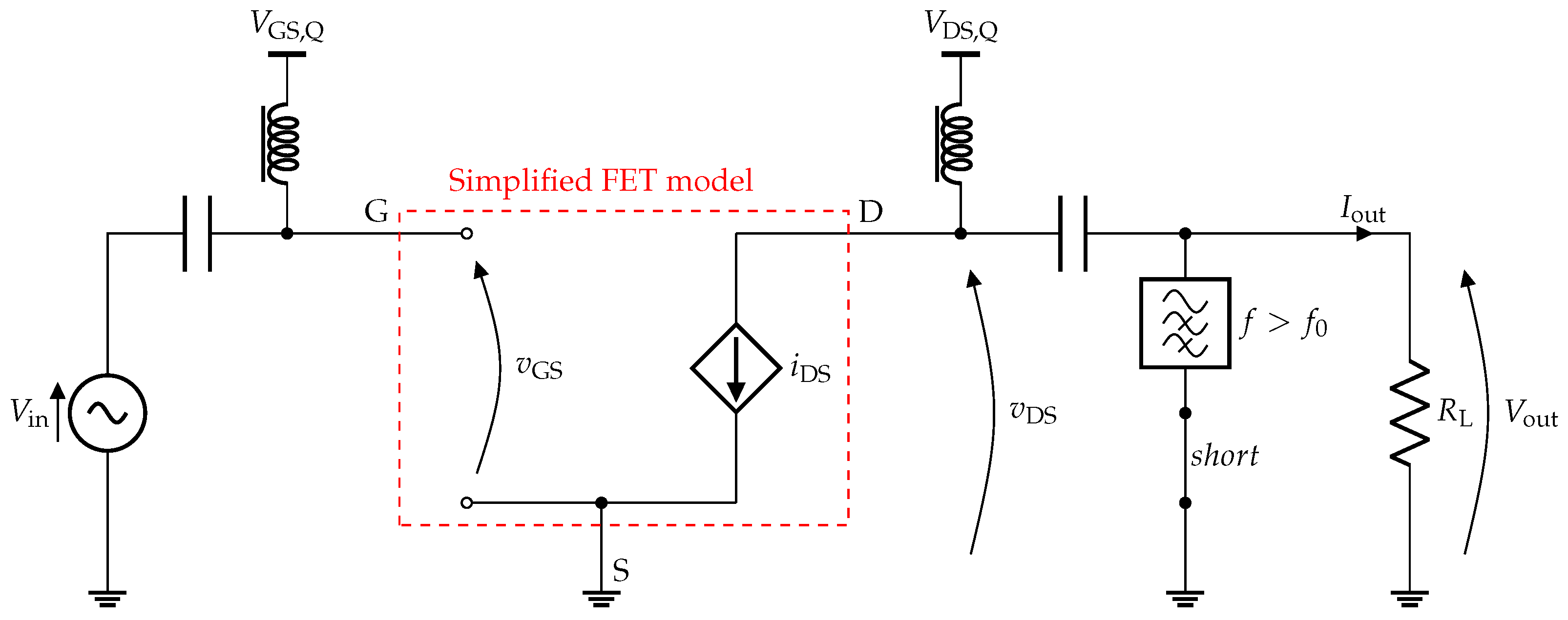
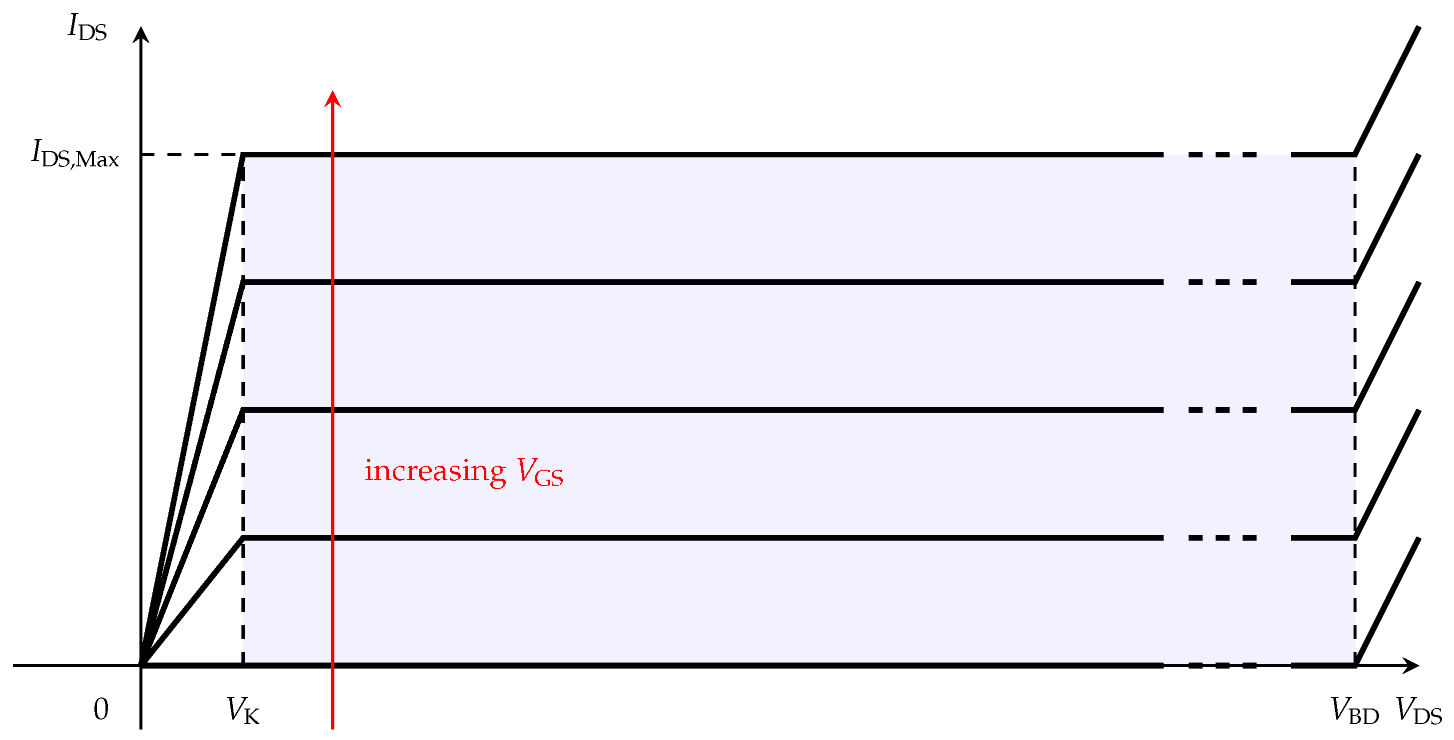
In current-mode FET-based PAs it is assumed that the active device acts as a voltage-controlled current source (VCCS) statically controlled by the gate-source voltage . The VCCS is assumed to be independent from the drain-source voltage , provided that the device is operating in the saturation region. Waveform clipping is the essential nonlinearity of an FET, thus the simplest and most widely adopted model for high-frequency FET devices, called strongly nonlinear model in [9], is a piece-wise linear trans-characteristic which considers zero drain-source current (full cut-off) below pinch-off, i.e., for input voltages lower than the threshold voltage , a linear relationship between the input voltage and the drain-source current above pinch-off, i.e., a constant transconductance , up to a certain and then hard current saturation/clipping to a maximum value , as shown in Figure 2. Hence the drain-source current is bounded between zero (whenever ) and (whenever ). This model is valid for n-type FETs, which are the most widely adopted devices for high-frequency applications thanks to the higher electron mobility compared to that of holes [33], while in p-type FETs the current is zero above pinch-off and follows a linear relationship below pinch-off. The threshold voltage is negative in depletion-mode (D-mode) FETs and positive for enhancement-mode (E-mode) ones. In the following, the n-type D-mode FET will be considered, since it is the most common high-frequency power device type (MESFETs, HEMTs).

Figure 2.
Bias points corresponding to the 4 possible biasing classes of Table 1 on the trans-characteristic. For the class-C case the equivalent negative current is also shown.
The input voltage, neglecting any possible input nonlinear effect, is assumed to be a pure sinusoid of the form
where and is the fundamental frequency, is the DC component of the input voltage, fixed by the gate supply battery, and is the peak amplitude of the input signal. The input voltage is periodic in with period and symmetrical around , where it reaches the maximum value, while the voltage minima are for . The maximum drain-source current is also reached at , while, due to pinch-off, the current minima may be clipped depending on the device bias point and input power level, yielding to a truncated sinusoid, with a zero current region corresponding to the swing of the input voltage below the threshold voltage. On the other hand, if the input voltage is increased above (over-driving operation), the drain-source current is clipped also at , and the waveform becomes that of Figure 1, approaching a square wave with increasing input power.
In practice, current clipping in a PA can be due not only to over-driving, i.e., pushing the input voltage above current saturation threshold, but also to input nonlinear effects, input harmonic shaping techniques, or, in cascaded PAs, to clipped input voltage resulting from previous-stage output clipping [49]. However, from a theoretical point of view, under the assumption of constant transconductance, all these cases can be treated by considering an equivalent over-driving condition.
As detailed in Figure 1, the values of for which the current reaches zero are , while those for which the current reaches are . The angle , i.e., the portion of the period for which the device is conducting current, is called conduction angle (or current conduction angle, CCA). The angle can be instead called saturation angle, since it corresponds to current saturation. The drain-source current can thus be written as
From (2) the saturation angle can be found as
where is the ratio between the actual amplitude of the RF current and that at the onset of the upper waveform clipping (see Figure 1). Thanks to the constant transconductance, it can be directly related to input power back-off () as
Therefore, with this model, upper waveform clipping arising for , which is also the range where the arccosine function is defined in the real domain (i.e., for arguments within , while, extending it to the complex domain, it is purely imaginary for arguments outside this range), is due to input power over-driving as in [9]. Nonetheless, as anticipated, given a clipped current waveform such as that in Figure 1, whatever the actual physical cause of upper clipping, an equivalent input over-driving level can be always mathematically defined. Again from (2), the conduction angle can be found as
where is the ratio between quiescent DC current and the maximum RF amplitude without upper waveform clipping , and it is thus a parameter related to the device bias point:
Clearly, exists only if the current is clipped at zero, which coincides with having which is again the range where the arccosine function is defined in the real domain.
The drain-source current, between pinch-off and saturation, can be therefore written as
The maximum RF current adopted to define and , depends in turn on the bias point, but it can be easily related to the saturated current as
Operating Class, Biasing Class and Parameter Space
There is often confusion about the terms biasing class and operating class. The former is uniquely defined by the selected bias point, while the latter takes into account both the instantaneous conduction angle, which is function of input power level, and the device harmonic loads. Therefore, for example a class-AB (biasing class) amplifier is “behaving like a class-A” (operating condition) in small-signal regime, as it does not show current clipping. However, considering the harmonic loading condition, even starting from the same biasing class, it is possible to further distinguish other operating classes, like, e.g., class-F (current-mode) or class-E (switching mode) [13].
Note from (5) that at , i.e., at current saturation limit when and hence at the maximum possible current without upper waveform clipping, the conduction angle is
The CCA at saturation is the parameter typically adopted in textbooks to define the biasing class. There are 4 possible biasing classes, as reported in Table 1 and in Figure 2 showing the position of the bias points on the trans-characteristic. Please note that for class-C devices, it is possible to define an equivalent negative proportional to the selected .

Table 1.
Features of the different current-mode biasing classes.
As can be noted from Table 1, the parameter is positive for class-A and class-AB biases, zero for class-B bias and negative for class-C bias, and ranges from 1, corresponding to class-A, to , which correspond instead to the case , i.e., to a device that never conducts current (OFF device). Please note that while is a strict limit, is not, as in principle it is possible to go up to , which corresponds to a constant . However, there is no practical interest in setting the quiescent DC current to values higher than (class-A). The parameter instead is clearly positive, and the overall parameter space of the analysis is that reported in Figure 3.

Figure 3.
Parameter space.
As anticipated, exists only if the current is clipped at , i.e., if , while exists only if the current is clipped at zero, i.e., if . The case corresponds to a class-C-biased device below current conduction threshold , that is found by posing
For the conduction angle can be considered constant at the limit value
The case corresponds instead to a class-AB-biased device that is behaving as if it were in class A, i.e., has purely sinusoidal current. This happens below the current-clipping threshold , which is found by posing
For the conduction angle can be considered constant at the limit value
Concerning instead the saturation angle, from (no RF input) up to current saturation () the argument of the arccosine is higher than unity and thus it can be considered constant at the limit value
The above considerations are confirmed by the current waveforms reported in Figure 4. For a class-A device (Figure 4a), the drain-source current remains a pure sinusoid () up to , then, for higher values shows a symmetrical current clipping. For a class-B device (Figure 4c) the current is a half-sinusoid (), and an asymmetrically clipped waveform for , while for a class-AB device (Figure 4b) the waveform is a pure sinusoid for , i.e., when , while it is clipped for higher input power levels. Finally, for a class-C device (Figure 4d) the current is zero for , i.e., when . Clearly, in all cases, in the limit of infinitely large RF input power () the output waveform tends to a square wave (yellow curves), which means .

Figure 4.
Normalized drain-source current at different . Dashed lines show the mathematical sinusoids that define the waveforms from which the peak current can be appreciated.
3. Generalized Harmonic Analysis
The drain-source current is an even function of , therefore it can be expanded into a Fourier series containing only cosine terms
where
Having introduced the parameters and in (6) and (4), respectively, and using (8), the drain-source current can be re-written as
hence the Fourier coefficients can be computed as
The two integrals appearing in (18) are
and
hence, in the most general case of , the Fourier coefficients in trigonometric form are
Substituting now the expressions of and of (5) and (3) the trigonometric expressions of (21) can be written as explicit functions of and . For and the conversion is straightforward, since and . For , to deal with and , we resort to first and second-order Chebyshev polynomials [50]. For , the latter are given by
therefore
Adopting the above equation together with (8), the final expressions for the Fourier coefficients of the drain-source current, normalized with respect to (i.e., ), as a function of and are
The DC and fundamental-tone coefficients and , here reported separately for convenience, can be obtained from the general expression of as shown in Appendix A. The equations of (24) are defined in the real domain only in the region of the parameter space in Figure 3. For the square-root and the arccosine functions are defined only in the complex domain. The most general expression, in the complex domain, for the Fourier coefficients are thus
Since not all mathematical CAD tools implement complex domain functions, it is convenient to explicitly write the explicit expression for . In particular, for region, i.e., when the waveform is clipped only at zero level, the equations simplify to
For (class-AB below clipping threshold) the coefficients simplify to
while for (class-C below conduction threshold) it is clearly . Please note that these expressions can be found by substituting the limit values of (14), (13) and/or (11) into (21).
Finally, it is useful to understand what happens in the limit case of square-wave current, i.e., when
This condition can be mathematically modeled with infinite input over-driving, i.e., by taking the limit of (24) for (marked as a yellow dashed line in the parameter space of Figure 3). The complete calculations are reported in Appendix B, the result is
Please note that as expected, the current contains only odd harmonics, which have alternating sign (the third harmonic is negative, the fifth is positive and so on).
Figure 5 and Figure 6 report, as an example, the first three harmonic components of the current, normalized to . As expected, the DC value of a class-A device remains constant while that of a class-B increases linearly up to . Up to current saturation, the fundamental current component increases linearly with input power in the case of class-A and class-B biases, while in class-AB and in class-C there is a slope change which is responsible for gain compression/expansion. Upper clipping makes the DC and fundamental tones keep increasing monotonically with input power, saturating rather quickly at the square-wave-limit value. Higher harmonics undergo instead a sudden slope change and show a non-monotonic (but rather oscillating) behavior before reaching their limit values. Finally, it is worth noting that all odd harmonics are the same for a class-A and a class-B PA.
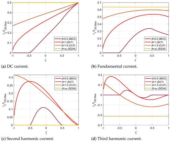
Figure 5.
Normalized components of the drain-source current as a function of .
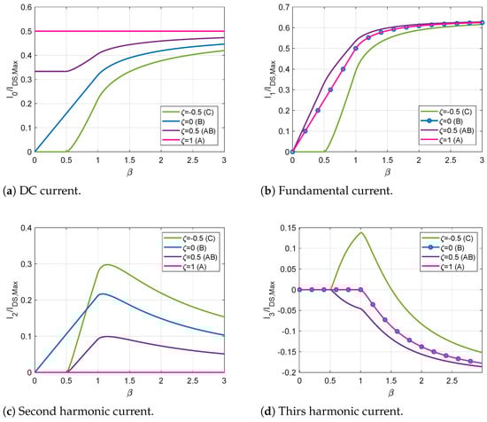
Figure 6.
Normalized components of the drain-source current as a function of .
From the current coefficients found in (24) it is possible to compute the most relevant PA performance, such as output power, efficiency, gain and dissipated power. To this aim, however, the output voltage must be considered, which in turn depends on the loading condition of the specific amplifier that is being analyzed. As an example, some results concerning the simplest tuned-load PA are reported in the next Section. Having access to all Fourier components at all possible input power level (or equivalent input power level in the case of clipped current) and for all possible biasing classes helps in extending the analysis to harmonic tuned and to load-modulated PA architectures, obtaining a better insight of the PA behavior as a function of input power.
4. PA Analysis Example: Tuned-Load PA Performance
The basic scheme of a tuned-load PA, neglecting all intrinsic and parasitic reactances is shown in Figure 7. Since the output resonator shunts all harmonics across the VCCS but the fundamental, the output voltage is a pure sinusoid at the fundamental frequency centered around the quiescent DC voltage , fixed by the drain supply battery. In this simplified analysis ideal harmonic shorts are considered; however, this assumption is approximately true also in actual implementations. The intrinsic low-pass behavior of the active device prevents power to be delivered to harmonics higher than the fifth. For the first three or four harmonic frequencies, harmonic traps can be explicitly included [51], but more frequently, low-pass-type output matching network are adopted to remove higher harmonics while simultaneously provide optimum load at fundamental [52].
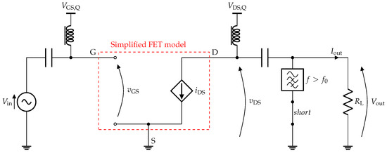
Figure 7.
Tuned-load power amplifier: one or more parallel shunt resonators allow only the fundamental component of the output voltage to flow into the resistive load .
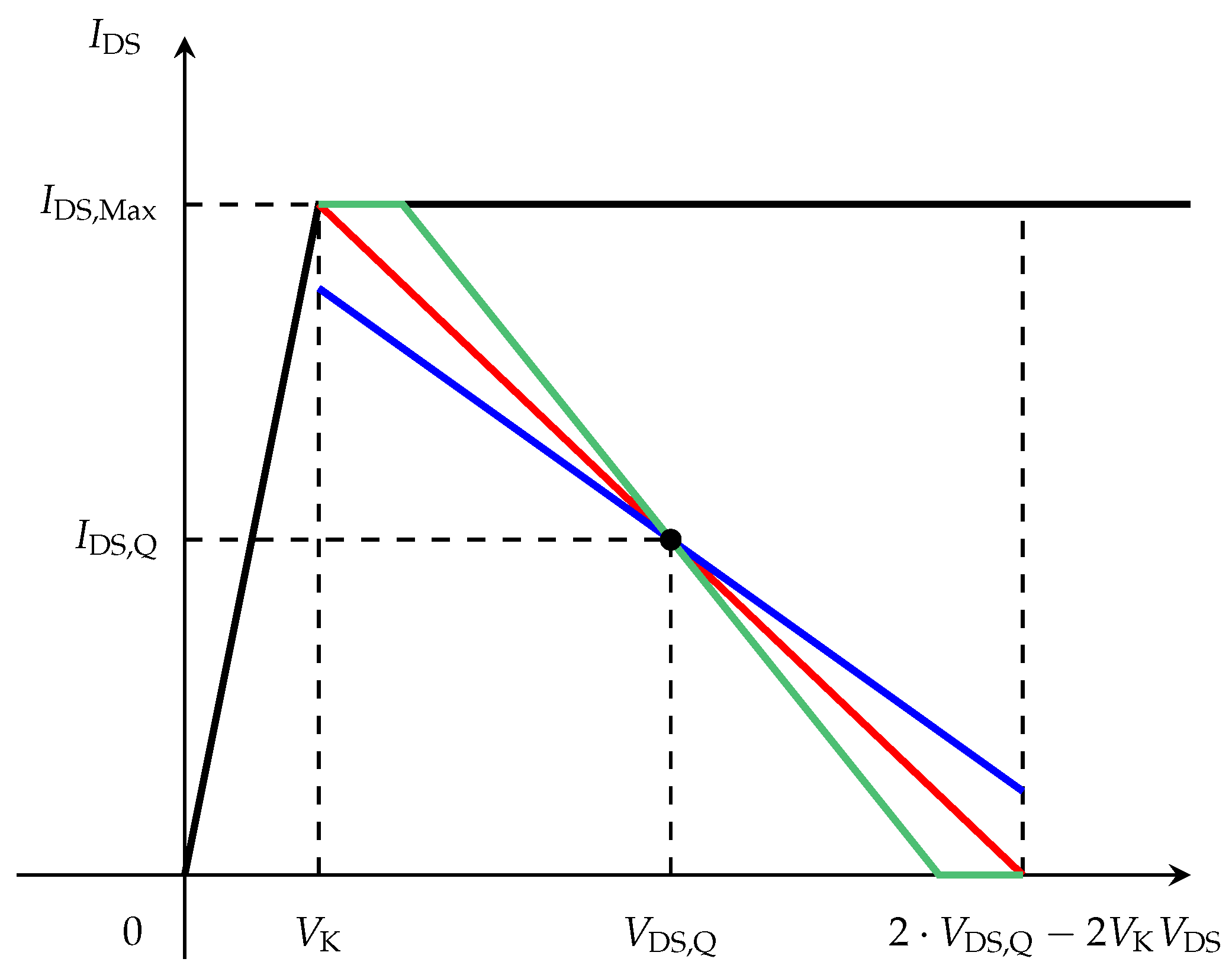
The optimum load is the load that maximizes simultaneously the output current and voltage swings, hence maximizing output power. According to the VCCS model, the maximum (peak-to-peak) current swing is , while concerning voltage, the simplified DC-IV characteristics shown in Figure 8 are considered in this analysis. This model is called box model in [13] since both drain-source current and voltage are bounded at both sides. Toward low values, the voltage limit is defined by the knee voltage, which marks the transition between the ohmic and saturation regions. Toward high values, instead, the limit is represented by the drain-source breakdown voltage . In this simplified model, both and are considered independent from the bias point, which is an approximation, while the assumption of constant-transconductance results in equally spaced output characteristics.

Figure 8.
Output DC-IV characteristics of the simplified box model of an n-type D-mode FET.
In principle, in order not to exceed the voltage limits at the maximum current, the quiescent voltage should be set at the mid-point between the two boundaries so that the maximum swing is . However, in practice, real devices typically have breakdown voltages significantly higher than the usable range of values, thus the breakdown limit may be neglected, and the quiescent voltage can be fixed accounting only for the knee-voltage limit. The maximum (peak-to-peak) voltage swing is thus
where
is a parameter representing the non-ideality due to a non-zero knee voltage [13]. Clearly, in this case, in order not to exceed the voltage limits at the maximum current, and the load , which relates the fundamental components of the output current and voltage, must be selected consistently.
The load relates the voltage and current swings, and the optimum load is classically defined as the resistance value that allow simultaneous maximum current and voltage swings, hence maximum output power. Clearly with a fixed resistance, simultaneous maximum current and voltage swings can be reached only at one specific input power level, corresponding to a specific value of that will be denoted as in the rest of the analysis. Once selected the value of , the optimum load resistance is sized as
where and are, respectively, the absolute and normalized amplitude of the fundamental current at . As an example, Figure 9 reports the load lines obtained for a class-A amplifier, by sizing at different values of . Most PAs are designed to work at the current saturation limit as the best compromise between output power and linearity, thus, typically, (red curve). However, to enhance linearity and/or to deal with non-constant envelope signals, the maximum power level may be reduced, which means using (blue curve). Finally, if the device is planned to be operated with clipped drain-source current, the value of corresponding to the equivalent over-driving level should be adopted (green curve).
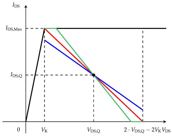
Figure 9.
Load-lines for a TL class-A PA with sized at different : (max. swings without clipping, red), (limited current swing, blue), (current clipping, green).
The saturated class-A PA, i.e., the case , is typically considered to be the reference for normalization. In this case, , thus the optimum load resistance is
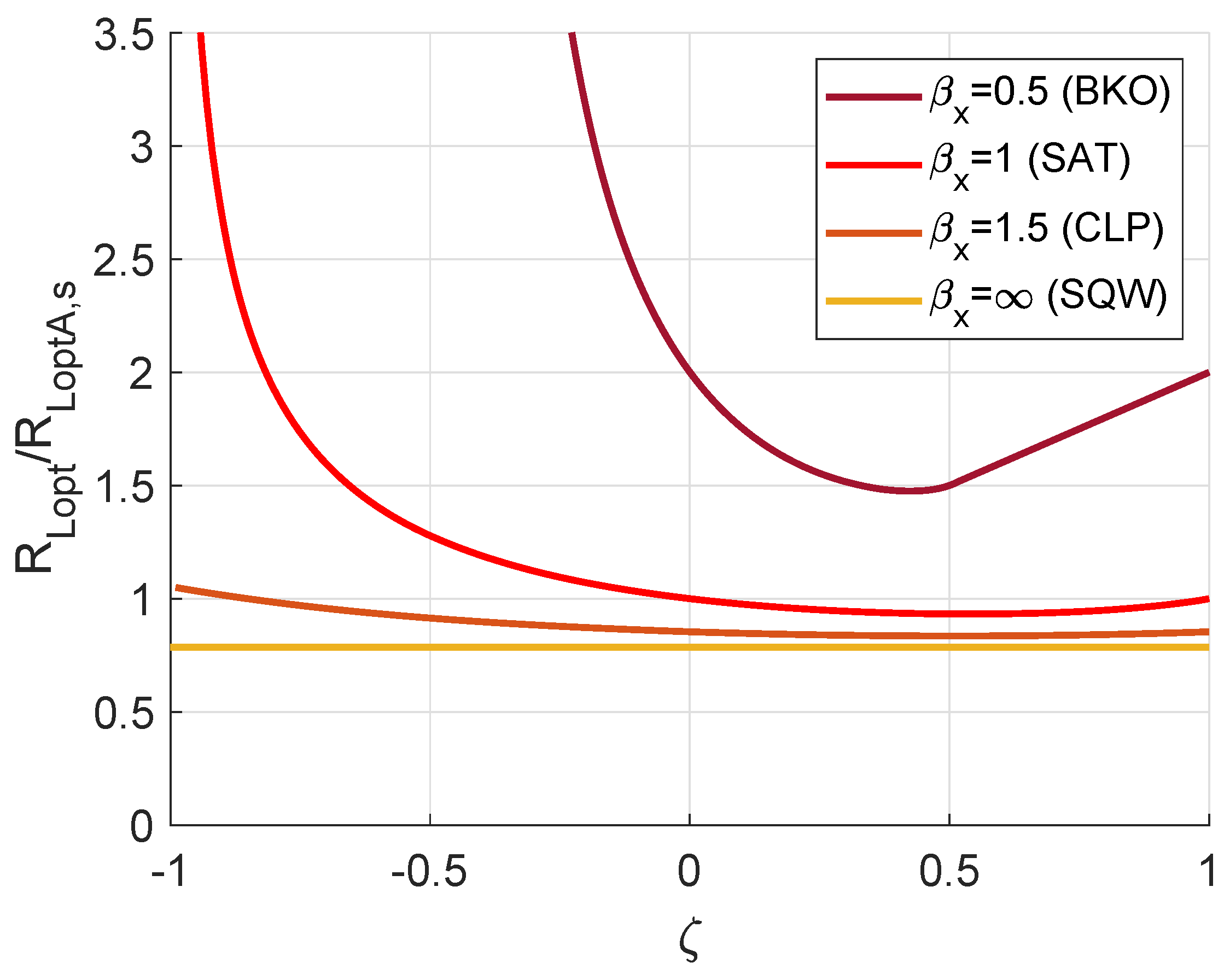
Therefore, it is possible to write the normalized optimum resistance as
Figure 10 reports the results of this equation as a function of , for different choices. The red curve is the classical textbook curve for PAs designed to operate at current saturation limit ().
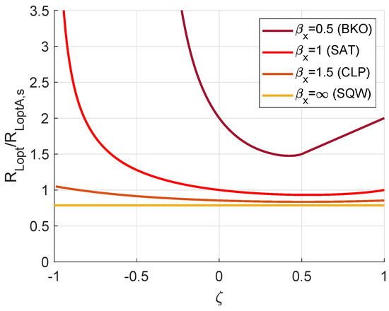
Figure 10.
Normalized optimum load resistance as a function of the biasing class for different choices.
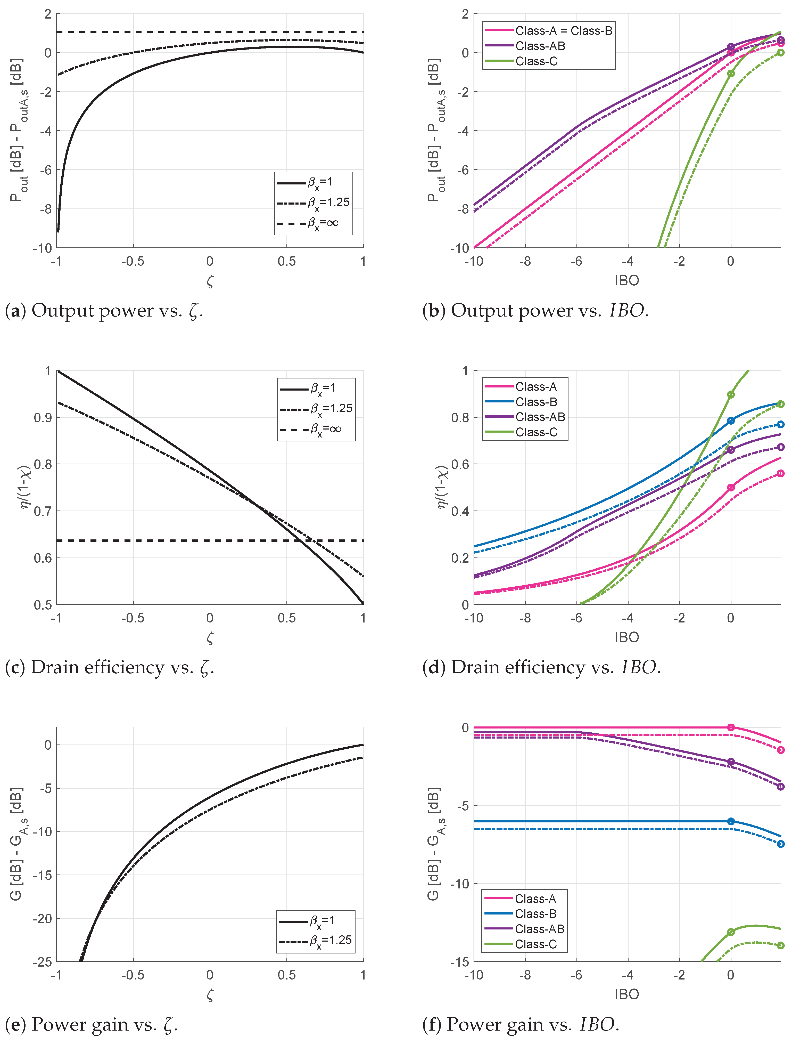
Once fixed bias and load, all PA features can be obtained from the harmonic current coefficients of (24). The output DC power is given by
The output RF power is non-zero only at the fundamental frequency and it is
where is the output power of the reference class-A PA at maximum current without clipping. Drain efficiency is defined as an thus it results
where we normalized with respect to the knee-voltage correction defined in (30) The operating power gain is defined as
and it is a very important figure of merit of a PA since, from it, it is possible to assess linearity (i.e., how linear is the relationship between input and output power), but also to compute the power added efficiency ()
and hence the dissipated power
which is in turn related to device channel temperature
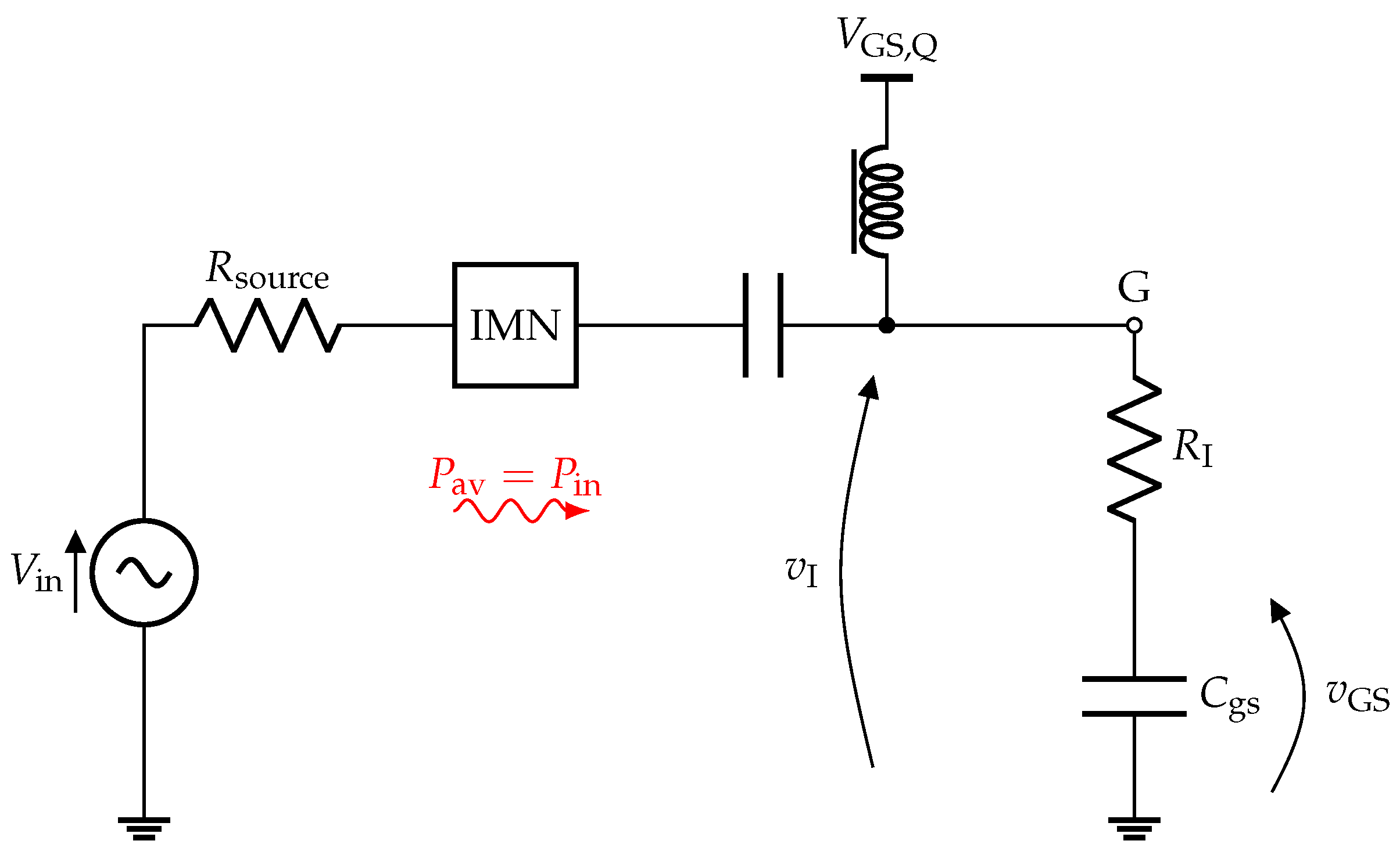
which is a fundamental aspect in many applications, for example in space environment [53]. The simplified FET model in Figure 7 assumes an open-circuit gate and the entire across gate and source terminal as the controlling voltage of the VCCS. Clearly, such a model, has zero input power, and hence infinite gain. In PAs where the power gain is actually very high, the input power is negligible with respect to the output one, thus the model is a valid approximation and power added efficiency can be approximated by the drain efficiency () in the above equations. However, if the gain is relatively low, the input power must be taken into account in the analysis. To have a non-zero input power we need a finite input impedance with non-zero resistive part. The input impedance of an FET device is typically modeled by a series RC, with the controlling voltage taken only across the input intrinsic capacitance , as shown in Figure 11, which we assume to be constant with respect to input power. The input resistance is what accounts for power sink at the input.

Figure 11.
Input section of the TL PA adopting the quasi-static FET model.
As indicated in Figure 11, the controlling voltage of the VCCS, , is not the total gate-source voltage (). However, the relationship between them is simply given by a complex constant coefficient :
The input power is thus given by
where is the complex (constant) input admittance thus the input power is related to the input voltage by a (real) constant coefficient k. Since
we can finally write
and
where, again, and are the reference input power and gain of a class-A amplifier at . For example, for the plots in Figure 12 are obtained where it is possible to appreciate all the results expected from theory [13]: in a class-A PA the gain is constant while in a class-B PA , i.e., the gain is 6 dB lower than that of a class-A PA. Class-AB PAs undergo soft gain compression before reaching current saturation, instead, class-C PAs show gain expansion, while above , in all cases gain compression shows the same slope.

Figure 12.
Linearity for different biasing classes. Dashed lines are other intermediate class-AB (purple) and class-C (green) cases.
From the gain equations, the power added efficiency, dissipated power and channel temperature can be computes. For these quantities it is not convenient to perform normalization with respect to the reference case. However, in practice, since the physical device parameters are known, absolute plots can be easily obtained for all possible PA’s figures of merit from the current coefficients of (24).
4.1. Load Modulation
From Figure 9 it is clear that if one could seamlessly set the optimum loads at the corresponding level, i.e., adjusting it for any different current amplitude, the device would keep operating at constant maximum voltage swing at any power levels, hence maximizing output power and efficiency. This is the basis of the load modulation approach, which is the basis of the widely adopted Doherty power amplifier [31]. It consists of varying as a function of input power, to have maximum voltage swing in a continuous range of output power. Ideally, the load should follow instantaneously the current amplitude , i.e., it must be
as reported in Figure 13.
Figure 13.
Load modulation as a function of .
Under ideal load modulation power and efficiency become
and
As shown in Figure 14, the load modulation approach ensures highest possible efficiency in back-off, for all biasing classes. In particular, for a class-B PA the efficiency becomes constant. Textbook Doherty PAs, using a class-B PAs as Main device, show in fact constant efficiency in the Doherty region [13]. On the other hand, actual PA designs typically exploit class-AB Main PAs [52,54], thus showing a non-constant back-off efficiency.
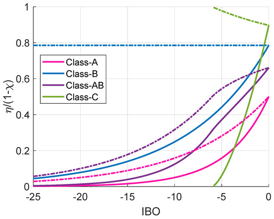
Figure 14.
Normalized drain efficiency with (, dash-dot lines) and without ( fixed, solid lines) load modulation for different operating classes.
The power gain under ideal load modulation becomes
which is monotonically decreasing from small signal up to current saturation, implying worse linearity.
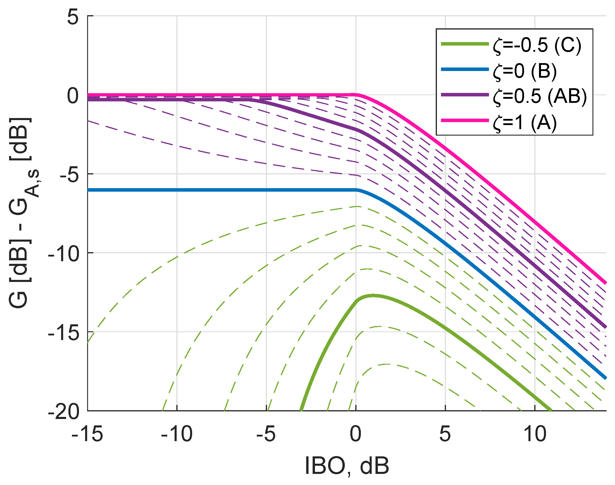
4.2. Over-Driving (Upper Current Clipping)
As demonstrated in [7,9], over-driving, or in general, the use of a clipped current waveform up to the limit case of a square-wave, can improve output power and efficiency at the expense of linearity. The analysis in [7,9], however is carried out for the case of broadband load, i.e., assuming a constant termination at all harmonics. In this case, the voltage waveform is a replica of the current one and thus it is also clipped, with consequent voltage harmonic generation. As discussed before, in the tuned-load case, it is not possible to drive the device at a power level higher than the one selected to size the load () otherwise the knee-voltage limit would be exceeded. From (28), sizing the optimum load considering square-wave current results in
i.e., a smaller resistance with respect to the broadband load must be adopted, yielding to
and
For a square-wave current, the output power is up to 1.05 dB higher than the reference case. The drain efficiency, which in the broadband load case approaches 81%, in the tuned-load case reaches only nearly 64%, thus is lower that the class-B efficiency at due to the required resistance reduction. Figure 15 compares the tuned-load PA performance at (current saturation limit), (moderate current clipping) and (square-wave current).

Figure 15.
Saturated (, solid lines) vs. over-driven (, dashed lines) PA performance. Circles in the right plots represent the maximum operating points.
5. Conclusions
A simple yet rigorous and comprehensive theoretical analysis of current-mode power amplifiers has been presented in this paper. Both power back-off and current-clipping scenarios have been taken into account, achieving compact analytical formulas for the current harmonic coefficients as functions of both bias point and input power back-off. From these coefficients it is possible to compute the most relevant performance of any PA architecture, once the harmonic input and output loading conditions are defined. As an example, the tuned-load PA case has been reported. The analysis is carried out assuming a constant-transconductance FET model, but it is prone to be extended to more realistic models, considering, e.g., higher order transconductance models or the current behavior in the ohmic region.
Author Contributions
Conceptualization, review and editing, all authors; original draft preparation, C.R.; investigation and formal analysis, C.R. and M.P.; supervision, P.C. All authors have read and agreed to the published version of the manuscript.
Funding
This received no external funding.
Institutional Review Board Statement
Not applicable.
Informed Consent Statement
Not applicable.
Conflicts of Interest
The authors declare no conflict of interest.
Appendix A
This appendix reports the prove that
In both cases the limit is a form that can be solved by expanding the numerator of to a first order Taylor series. The expression
is replaced with
therefore
and
Appendix B
This appendix reports the prove that
To solve these limits, it is necessary to resort to Taylor series expansion of the arccosine function and of the Chebyshev polynomials. For and , adopting
it is easy to show that
and
For , adopting
and
the combination of and that appears in becomes
thus
References
- Raab, F.; Asbeck, P.; Cripps, S.; Kenington, P.; Popovic, Z.; Pothecary, N.; Sevic, J.; Sokal, N. Power amplifiers and transmitters for RF and microwave. IEEE Trans. Microw. Theory Tech. 2002, 50, 814–826. [Google Scholar] [CrossRef] [Green Version]
- Terman, F.; Ferns, J. The Calculation of Class C Amplifier and Harmonic Generator Performance of Screen-Grid and Similar Tubes. Proc. Inst. Radio Eng. 1934, 22, 359–373. [Google Scholar] [CrossRef]
- Scott, T. Tuned Power Amplifiers. IEEE Tran. Circ. Theory 1964, 11, 385–388. [Google Scholar] [CrossRef]
- El-Said, M. Analysis of tuned junction-transistor circuits under large sinusoidal voltages in the normal domain-Part I: The effective hybrid-pi equivalent circuit. IEEE Trans. Circuit Theory 1970, 17, 8–12. [Google Scholar] [CrossRef]
- El-Said, M. Analysis of tuned junction-transistor circuits under large sinusoidal voltages in the normal domain-Part II: Tuned power amplifiers and harmonic generators. IEEE Trans. Circuit Theory 1970, 17, 13–18. [Google Scholar] [CrossRef]
- Griffin, E. Application of Load-line Simulation to Microwave High Power Amplifiers. Microw. Mag. 2000, 1, 58–66. [Google Scholar]
- Bahl, I.; Bhartia, P. Microwave Solid State Circuit Design; Wiley: Hoboken, NJ, USA, 2003. [Google Scholar]
- Colantonio, P.; Giannini, F.; Limiti, E. Nonlinear approaches to the design of microwave power amplifiers. Int. J. RF Microw. Comput.-Aided Eng. 2004, 14, 493–506. [Google Scholar] [CrossRef]
- Cripps, S. RF Power Amplifiers for Wireless Communications; Artech House Microwave Library, Artech House: Norwood, MA, USA, 2006. [Google Scholar]
- Cripps, S. A Theory for the Prediction of GaAs FET Load-Pull Power Contours. In Proceedings of the 1983 IEEE MTT-S International Microwave Symposium Digest, Boston, MA, USA, 31 May–3 June 1983; pp. 221–223. [Google Scholar] [CrossRef]
- Quaglia, R. Power amplifier design considerations using a simplified model for the transistor. In Proceedings of the 2021 IEEE MTT-S International Wireless Symposium (IWS), Nanjing, China, 23–26 May 2021; pp. 1–3. [Google Scholar] [CrossRef]
- Cripps, S. Advanced Techniques in RF Power Amplifier Design; Artech House Microwave Library, Artech House: Norwood, MA, USA, 2002. [Google Scholar]
- Colantonio, P.; Giannini, F.; Limiti, E. High Efficiency RF and Microwave Solid State Power Amplifiers; Microwave and Optical Engineering; Wiley: Hoboken, NJ, USA, 2009. [Google Scholar]
- Quaglia, R.; Shepphard, D.J.; Cripps, S. A Reappraisal of Optimum Output Matching Conditions in Microwave Power Transistors. IEEE Trans. Microw. Theory Tech. 2017, 65, 838–845. [Google Scholar] [CrossRef] [Green Version]
- Raffo, A.; Vadalà, V.; Bosi, G.; Trevisan, F.; Avolio, G.; Vannini, G. Waveform engineering: State-of-the-art and future trends. Int. J. RF Microw. Computer-Aided Eng. 2017, 27, e21051. [Google Scholar] [CrossRef] [Green Version]
- Colantonio, P.; Giannini, F.; Giofrè, R.; Piazzon, L. A Design Technique for Concurrent Dual-Band Harmonic Tuned Power Amplifier. IEEE Trans. Microw. Theory Tech. 2008, 56, 2545–2555. [Google Scholar] [CrossRef]
- Cipriani, E.; Colantonio, P.; Giannini, F. The effect of 2nd harmonic control on power amplifiers performances. In Proceedings of the 2012 7th European Microwave Integrated Circuits Conference (EuMIC), Amsterdam, The Netherlands, 29–30 October 2012; pp. 345–348. [Google Scholar]
- Ghisotti, S.; Pisa, S.; Colantonio, P. S Band Hybrid Power Amplifier in GaN Technology with Input/Output Multi Harmonic Tuned Terminations. Electronics 2021, 10, 2318. [Google Scholar] [CrossRef]
- Roblin, P.; Chang, H.C.; Gomez-Perez, J.M.; Martinez-Lopez, J.I. Generalized Class-J Theory. In Proceedings of the 2018 IEEE MTT-S Latin America Microwave Conference (LAMC 2018), Arequipa, Peru, 12–14 December 2018; pp. 1–3. [Google Scholar] [CrossRef]
- Nasri, A.; Estebsari, M.; Toofan, S.; Piacibello, A.; Ramella, C.; Camarchia, V.; Pirola, M. A 3-3.8 GHz Class-J GaN HEMT Power Amplifier. In Proceedings of the 2020 23rd International Microwave and Radar Conference (MIKON), Warsaw, Poland, 5–8 October 2020; pp. 416–419. [Google Scholar] [CrossRef]
- Iqbal, M.; Piacibello, A. GaN HEMT based class-F power amplifier with broad bandwidth and high efficiency. In Proceedings of the 2016 International Conference on Integrated Circuits and Microsystems (ICICM), Chengdu, China, 23–25 November 2016; pp. 131–134. [Google Scholar] [CrossRef]
- Sharma, T.; Darraji, R.; Ghannouchi, F.; Dawar, N. Generalized Continuous Class-F Harmonic Tuned Power Amplifiers. IEEE Microw. Wirel. Compon. Lett. 2016, 26, 213–215. [Google Scholar] [CrossRef]
- Cipriani, E.; Colantonio, P.; Giannini, F.; Giofrè, R. Class F-1 PA: Theoretical aspects. In Proceedings of the 2010 Workshop on Integrated Nonlinear Microwave and Millimeter-Wave Circuitsm, Gothenburg, Sweden, 26–27 April 2010; pp. 29–32. [Google Scholar] [CrossRef]
- Thian, M.; Fusco, V.F. Analysis and Design of Class-E3F and Transmission-Line Class-E3F2 Power Amplifiers. IEEE Trans. Circuits Syst. I 2011, 58, 902–912. [Google Scholar] [CrossRef]
- Moon, J.; Jee, S.; Kim, J.; Kim, J.; Kim, B. Behaviors of Class-F and Class-F-1 Amplifiers. IEEE Trans. Microw. Theory Tech. 2012, 60, 1937–1951. [Google Scholar] [CrossRef]
- Poluri, N.; De Souza, M.M. High-Efficiency Modes Contiguous With Class B/J and Continuous Class F-1 Amplifiers. IEEE Microw. Wirel. Compon. Lett. 2019, 29, 137–139. [Google Scholar] [CrossRef]
- Moon, J.S.; Moyer, H.; Macdonald, P.; Wong, D.; Antcliffe, M.; Hu, M.; Willadsen, P.; Hashimoto, P.; McGuire, C.; Micovic, M.; et al. High efficiency X-band class-E GaN MMIC high-power amplifiers. In Proceedings of the 2012 IEEE Topical Conference on Power Amplifiers for Wireless and Radio Applications, Santa Clara, CA, USA, 15–18 January 2012; pp. 9–12. [Google Scholar] [CrossRef]
- Nguyen, D.P.; Pham, A.V. An Ultra Compact Watt-Level Ka-Band Stacked-FET Power Amplifier. IEEE Microw. Wireless Compon. Lett. 2016, 26, 516–518. [Google Scholar] [CrossRef] [Green Version]
- Piacibello, A.; Pirola, M.; Camarchia, V.; Ramella, C.; Quaglia, R. A Ku-band Compact MMIC PA based on Stacked GaAs pHEMT cells. In Proceedings of the 2018 International Workshop on Integrated Nonlinear Microwave and Millimetre-Wave Circuits (INMMIC), Brive La Gaillarde, France, 5–6 July 2018; pp. 1–3. [Google Scholar] [CrossRef]
- Ramella, C.; Pirola, M.; Florian, C.; Colantonio, P. Space-Compliant Design of a Millimeter-Wave GaN-on-Si Stacked Power Amplifier Cell through Electro-Magnetic and Thermal Simulations. Electronics 2021, 10, 1784. [Google Scholar] [CrossRef]
- Ramella, C.; Piacibello, A.; Quaglia, R.; Camarchia, V.; Pirola, M. High Efficiency Power Amplifiers for Modern Mobile Communications: The Load-Modulation Approach. Electronics 2017, 6, 96. [Google Scholar] [CrossRef] [Green Version]
- Popovic, Z. GaN power amplifiers with supply modulation. In Proceedings of the 2015 IEEE MTT-S International Microwave Symposium, Phoenix, AZ, USA, 17–22 May 2015; pp. 1–4. [Google Scholar] [CrossRef]
- Ghione, G.; Pirola, M. Microwave Electronics; The Cambridge Rf And Microwave; Cambridge University Press: Cambridge, UK, 2018. [Google Scholar]
- Snowden, C.; Baets, R.; Barker, J.; Barnard, J.; Barton, T.; Clarke, M.; Cappy, A.; Howes, M.; Ingham, D.; Miles, R.; et al. Semiconductor Device Modelling; Springer: London, UK, 2011. [Google Scholar]
- Rugh, W. Nonlinear System Theory: The Volterra/Wiener Approach; Johns Hopkins Series in Information Sciences and Systems; Johns Hopkins University Press: Baltimora, MD, USA, 1981. [Google Scholar]
- Schreurs, D.; O’Droma, M.; Goacher, A.; Gadringer, M. RF Power Amplifier Behavioral Modeling; The Cambridge RF and Microwave Engineering Series; Cambridge University Press: Cambridge, UK, 2008. [Google Scholar]
- Wood, J. Behavioral Modeling and Linearization of RF Power Amplifiers; Artech House Microwave Library, Artech House: Norwood, MA, USA, 2014. [Google Scholar]
- Donati Guerrieri, S.; Ramella, C.; Bonani, F.; Ghione, G. Efficient Sensitivity and Variability Analysis of Nonlinear Microwave Stages Through Concurrent TCAD and EM Modeling. IEEE J. Multiscale Multiphysics Comput. Tech. 2019, 4, 356–363. [Google Scholar] [CrossRef]
- Curtice, W. A MESFET Model for Use in the Design of GaAs Integrated Circuits. IEEE Trans. Microw. Theory Tech. 1980, 28, 448–456. [Google Scholar] [CrossRef]
- Curtice, W.; Ettenberg, M. A Nonlinear GaAs FET Model for Use in the Design of Output Circuits for Power Amplifiers. IEEE Trans. Microw. Theory Tech. 1985, 33, 1383–1394. [Google Scholar] [CrossRef]
- Materka, A.; Kacprzak, T. Computer Calculation of Large-Signal GaAs FET Amplifier Characteristics. IEEE Trans. Microw. Theory Tech. 1985, 33, 129–135. [Google Scholar] [CrossRef]
- Kondoh, H. FET power performance prediction using a linearized device model. In Proceedings of the IEEE MTT-S International Microwave Symposium Digest, Long Beach, CA, USA, 13–15 June 1989; Volume 2, pp. 569–572. [Google Scholar] [CrossRef]
- Kushner, L.J. Output performance of idealized microwave power amplifiers. Microw. J. 1989, 32, 103. [Google Scholar]
- Kushner, L.J. Estimating power amplifier large signal gain. Microw. J. 1990, 33, 87. [Google Scholar]
- Angelov, I.; Zirath, H.; Rosman, N. A new empirical nonlinear model for HEMT and MESFET devices. IEEE Trans. Microw. Theory Tech. 1992, 40, 2258–2266. [Google Scholar] [CrossRef] [Green Version]
- Colantonio, P.; Giannini, F.; Leuzzi, G.; Limiti, E. Extensions of the Chalmers nonlinear HEMT and MESFET model. IEEE Trans. Microw. Theory Tech. 1996, 12, 2851–2855. [Google Scholar] [CrossRef]
- Angelov, I.; Bengtsson, L.; Garcia, M. Direct-synthesis design technique for nonlinear microwave circuits. IEEE Trans. Microw. Theory Tech. 1995, 44, 1664–1674. [Google Scholar] [CrossRef]
- Massobrio, G.; Antognetti, P. Semiconductor Device Modeling with SPICE; A McGraw-Hill Special Reprint Edition; McGraw-Hill Education: New York, NY, USA, 1998. [Google Scholar]
- Li, X.; Colantonio, P.; Giannini, F.; Yu, H.; Lin, C. S-Band Class-C-F Power Amplifier with 2nd Harmonic Control at the Input. Appl. Sci. 2020, 10, 259. [Google Scholar] [CrossRef] [Green Version]
- Mason, J.; Handscomb, D. Chebyshev Polynomials; CRC Press: Boca Raton, FL, USA, 2002. [Google Scholar]
- Colantonio, P.; Giannini, F.; Giofre, R.; Piazzon, L. GaN Doherty Amplifier With Compact Harmonic Traps. In Proceedings of the 2008 European Microwave Integrated Circuit Conference, Amsterdam, The Netherlands, 27–28 October 2008; pp. 526–529. [Google Scholar] [CrossRef]
- Giofrè, R.; Colantonio, P.; Giannini, F.; Ramella, C.; Camarchia, V.; Iqbal, M.; Pirola, M.; Quaglia, R. A comprehensive comparison between GaN MMIC Doherty and combined class-AB power amplifiers for microwave radio links. Int. J. Microw. Wireless Technol. 2016, 8, 673–681. [Google Scholar] [CrossRef]
- Ramella, C.; Pirola, M.; Reale, A.; Ramundo, M.; Colantonio, P.; Maur, M.A.D.; Camarchia, V.; Piacibello, A.; Giofrè, R. Thermal-aware GaN/Si MMIC design for space applications. In Proceedings of the 2019 IEEE International Conference on Microwaves, Antennas, Communications and Electronic Systems (COMCAS), Tel-Aviv, Israel, 4–6 November 2019; pp. 1–6. [Google Scholar] [CrossRef] [Green Version]
- Colantonio, P.; Giannini, F.; Giofrè, R.; Piazzon, L. The AB-C Doherty power amplifier. Part I: Theory. Int. J. RF Microw. Computer-Aided Eng. 2009, 19, 293–306. [Google Scholar] [CrossRef]


Publisher’s Note: MDPI stays neutral with regard to jurisdictional claims in published maps and institutional affiliations. |
© 2021 by the authors. Licensee MDPI, Basel, Switzerland. This article is an open access article distributed under the terms and conditions of the Creative Commons Attribution (CC BY) license (https://creativecommons.org/licenses/by/4.0/).