1. Introduction
Because the flyback converter has a simple structure and does not require a secondary side output inductor, it has considerable advantages in size and cost. Based on the above advantages, the flyback converter is widely used in low power applications [
1,
2,
3,
4,
5,
6,
7,
8,
9,
10,
11,
12,
13,
14,
15,
16]—especially in LED lighting [
8,
9,
10] and battery balancing control [
11,
12,
13,
14,
15,
16] to show its many advantages. With the advancement of digital technology and the cost of microcontrollers has dropped significantly. The control scheme of flyback is also moving towards digital control to obtain higher performance [
17,
18,
19,
20]. Since the flyback converter is an isolated converter, the output voltage and current are traditionally regulated by utilizing the secondary-side regulation (SSR). Usually, SSR is mainly constructed by a photocoupler. The photocoupler feedback circuit causes above 10% of the power losses at standby conditions. Recently, primary-side regulation (PSR) flyback converter (i.e., primary-side controlled flyback converter) becomes an important technology due to lower cost and standby power losses [
1,
17,
18,
19,
20,
21,
22,
23,
24,
25]. The primary-side controlled flyback converter stores energy on the transformer when the power switch is ON and releases the energy on the transformer to the load when the power switch is OFF. It is known that this topology is a constant power output. Based on the constant power output characteristics, when the output voltage of the flyback converter drops due to the load, the output current must increase. When the output voltage of the flyback converter keeps dropping, the current keeps increasing until the current is infinite, causing the problem of components burning. At the same output power, the higher input voltage results in a lower input current. On the contrary, the lower input voltage will result in a higher input current. This means that different power losses are caused by different input voltages, so a larger rated component must be selected in the circuit design to meet the range under various conditions.
As shown in
Figure 1, the conventional flyback converter has primary side peak current detection overcurrent protection. Because the primary-side peak current detection protection point voltage
VLIMIT is a fixed value, and the flyback converter working in Discontinuous Conduction Mode (DCM) has a constant power output as shown as [
22]
where
Lp, fsw, Ip and
η are the primary side inductance, switching frequency, primary side peak current, and flyback conversion efficiency, respectively.
When the load on the output terminal becomes larger and larger, the output voltage becomes lower. At this time, the output current will still be larger and larger as shown in Equation (2). Therefore, the current rating of the part needs to be selected with a larger specification, just to meet the protection application.
In order to overcome the above-mentioned problem, two methods were proposed and used in converters. In this first method, a current detection resistor Rsense is connected in series with the current loop at the output end to convert the current signal into a voltage signal. Then, use the comparison circuit or the current monitor IC to judge whether the overcurrent condition is reached. If the overcurrent condition is satisfied, turn off the synchronous rectification switch. Another method is to connect a current detection resistor Rsense in series with the ground current loop at the output end to convert the current signal into a voltage signal. Then, use the comparison circuit or the current detection IC to determine whether the overcurrent condition is occurring. If the condition is satisfied, the primary switch PWM duty is adjusted through the photocoupler control—to make the entire power supply achieve the functions of stability and overload protection. With these two methods, only a current detection resistor Rsense and comparison control circuit or current monitor IC are needed to achieve the purpose of current detection and protection. However, the current detection resistor Rsense is connected in series with the output main circuit. Because the current is large, in order to avoid excessive power loss, the current detection resistor is usually very small. The current detection resistance Rsense is generally between several mΩ to tens of mΩ, depending on the output current. Therefore, the converted voltage signal is about tens of mV and hundreds of mV. The accuracy of such a small voltage signal is obviously insufficient for judgment and control. In addition, the power loss caused by the current detection resistor Rsense under heavy load is inevitable.
In a typical primary-side controlled flyback converter, a sensing resistor R
S is used to convert the current on the primary side into a voltage
VS and compares it with the reference voltage
VLIMIT of the controller. When the sensing voltage
VS is greater than the reference voltage
VLIMIT, the comparator is activated to turn off the power switch. Unfortunately, in actual applications, due to the stray capacitance inside the semiconductor device, a fixed logic drive delay is caused. When the input voltage is high, the current slope
on the primary side becomes steeper. Due to the delay in the response time of the comparators, logic gates, and components, the power switch cannot be turned off immediately when the sensing voltage
VS is greater than
VLIMIT. As a result, the primary side current still maintains a fixed slope rise, and the overflow current
occurs and can be shown as [
22]
where
tdelay is the delay time that is the amount delay times of the comparators, logic gates, and other components.
Figure 2 shows a schematic diagram of overflow current
changes caused by signal delay under traditional peak current mode control. It can be seen that a higher input voltage
Vin has a larger overflow current
than a lower input voltage. This leads to a significant difference. When the input voltage is higher, the power that can be provided to the load is higher, and vice versa. This is one of the main reasons affecting line regulation of flyback converter.
In order to solve the above problem, many methods and techniques were proposed. The amount of overflow current
can be estimated by using the change of current in the same
tdealy time. According to this estimated value to modify the PWM, the influence of
tdealy can be reduced [
21]. Furthermore, the CS sample-and-hold circuit is used to measure primary side peak current
Ip. Then, by calculating the average current, a compensation control method that is theoretically unaffected by
tdealy can be obtained [
22]. Another method is to measure the mid-point current (i.e., average current) and use the average current control method, which can effectively reduce the influence of
tdealy and increase the accuracy of the output current [
23,
24,
25]. Recently, digital technology is also used to directly measure
tdealy. Finally,
tdealy is compensated to obtain accurate output current [
17,
20].
Although the above methods can be used to reduce the impact of
tdealy. However, when an overload occurs and the output voltage is reduced, the output current cannot be suppressed. Therefore, the current rating of the components needs to be selected with a larger specification, just to meet the protection application. In order to solve this problem, a Compensated Peak Current mode controlled PWM (CPC-PWM) for primary-side controlled flyback converters working in DCM is proposed in this paper. In the proposed CPC-PWM, the input voltage
Vin is sensed and can be used to compensate for the control signal delay to reduce the overflow current
to improve line regulation. In addition, the current limiting by voltage feedback scheme [
26,
27] is referenced. The output voltage
Vout of flyback is sensed and be used to compensate PWM to suppress the overload current.
2. System Description
In order to suppress the output current
Io of the flyback converter during overload protection, the feedback compensator (FBC) is proposed in this paper. The inherent characteristics of the flyback converter output voltage
Vout can be used to detect and adjust the PWM duty.
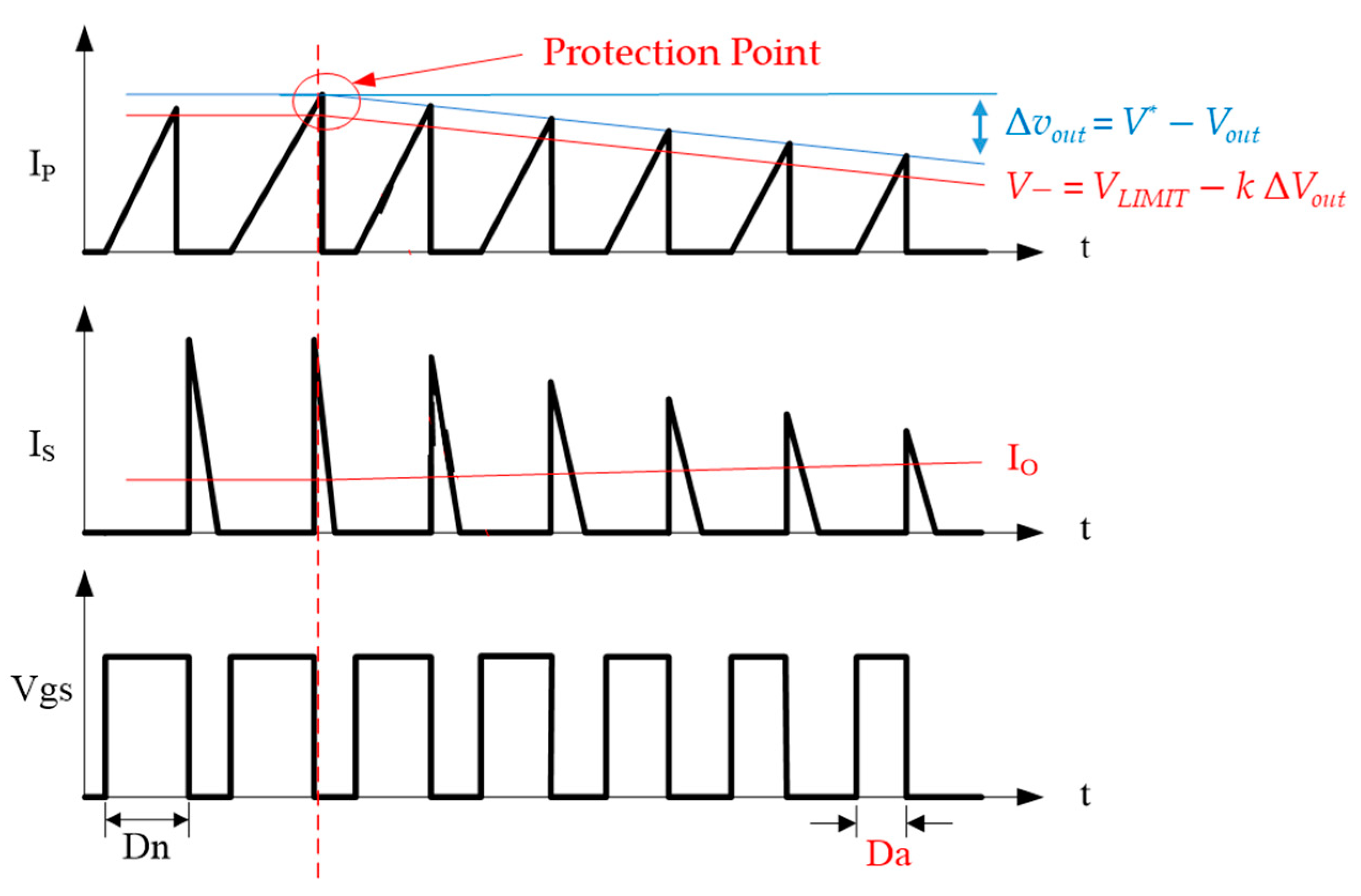
Figure 3 shows the waveforms of a primary-side controlled flyback with FBC control working in DCM. As shown in
Figure 3, when the output voltage
Vout drops, the power switch duty cycle needs to be reduced to suppress the output current
Io. This means that the PWM duty cycle
Da during abnormal operation should be much smaller than the PWM duty cycle
Dn during normal operation. The amount of this output voltage drop Δ
Vout is the difference between the rated output voltage
V* and the output voltage
Vout. Thus, the input voltage of the negative terminal of the comparator
V- will be compensated by the amount of this output voltage drop and written as:
where
k is a positive constant. A larger
k means a smaller duty cycle
Da is obtained. Equation (4) can be rewritten as:
where
k1,
k2, and
k3 are positive constant. It can be seen from (5) that when the output voltage
Vout drops more, the voltage
V− becomes smaller. This reduces the PWM duty cycle and achieves the purpose of suppressing the output current
Io.
Figure 4 shows the theory expected V-I curves of a flyback with and without FBC. Comparing the V-I curves of the traditional method and the proposed method, the output current of the proposed method is much lower. It means that there is no need to choose a power component with a larger current rating. In this way, the power consumption problem caused when the output load is increased or short-circuited can be suppressed, and the components with larger specifications can be avoided.
In order to suppress the overflow current
of the flyback converter, the FeedForward Compensator (FFC) is proposed in this paper. The input voltage
Vin of the flyback converter is detected and used to adjust the PWM duty, since the overflow current
is proportional to the input voltage
Vin shown as (3).
Figure 5 shows waveforms of a primary-side controlled flyback with FFC control working in DCM. As shown in
Figure 5, the input voltage of the positive terminal
V+ of the comparator is extract added by
Vin as written as:
Equation (6) can be rewritten as:
where
k4 and
k5 are positive constant. It is clear that when the input voltage
Vin increases, the voltage
V+ becomes larger. When
V+ becomes larger, the power switch
S1 will be turned off early. When (8) is held, the overflow current
caused by
tdelay is eliminated.
Based on the above discussion, the block diagram of the proposed CPC-PWM controller mentioned in this paper can be drawn as
Figure 6b. Compared with the traditional peak current mode control PWM shown in
Figure 6a, we can see that the FBC is added, thereby achieving the purpose of suppressing the output protection current. On the other hand, the FFC is also added, thereby suppressing the purpose of the overflow current
.
Design Example:
In order to verify the feasibility of the proposed CPC-PWM, a 5 W prototype is designed and realized. The specifications and circuit diagram of the prototype are listed and shown in
Table 1 and
Figure 7, respectively.
The flyback converter proposed in this paper is mainly constructed by a transformer, an FBC, an FFB, and a power switch
S1 as shown in
Figure 7. The transformer includes a primary winding, a secondary winding, and an auxiliary winding or third winding. The output voltage of the third winding is injected into the feedback compensator circuit to adjust the PWM duty of the power switch. FBC is composed of a diode
D1, four resistors
R1,
R2,
R3, and
R5, and three capacitors
C1,
C2, and
C3, as shown as a red block in
Figure 7. Due to the characteristics of the flyback converter, the energy is transferred to the secondary side when the power switch is turned off. At the same time, the third winding is used to sample the output voltage condition to obtain the voltage
VT. Due to the transformer leakage inductance, there will be a spike voltage and the voltage
VA can be obtained only after being processed by a low-pass filter. A first-order RC filter is used and meet to (9) to filter out spike voltage
where
tspike is the period of the spike voltage.
The feedback compensator is a network circuit and can be simplified as
Figure 8. The simplified circuit is composed of three voltage sources
VA,
Vref, and
VLIMIT, and four resistors
R2,
R3,
R5, and
R6. Voltage
V− can be obtained and shown as (10) by using KCL law. Compared with (5), parameters
k1,
k2, and
k3 can be obtained and shown as (11)–(13).
where
GX is the reciprocal of
RX, that is a conductance.
The FFC is a network circuit composed of two voltage sources
Vin and
Vs, and two resistors
R4 and
R7. Voltage V+ can be obtained and shown as (14) by using KCL law. Compared with (7), parameters
k4 and
k5 can be obtained and shown as (15) and (16). In addition, the relation between resistor
R4 and
R7 is shown as (17).
where
GX is the reciprocal of
RX, that is a conductance.
The used components of the designed flyback converter as shown in
Figure 7 are listed in
Table 2.
3. Experimental Results
The feasibility and superiority of the proposed method are verified by discussing and comparing “overload current variation”, “input power consumption during short circuit” and “overflow current variation”.
Figure 9a–c shows the V-I curves obtained by using the traditional peak current control.
Figure 9d–f shows the V-I curves obtained by using the proposed FBC method.
It can be seen from
Figure 9a–c that the V-I curve has an obvious relationship with the input voltage
Vin. When the input voltage
Vin is higher, the overload point will also be higher.
Figure 9d–f shows the V-I curves obtained using the proposed FBC method. It can be seen that when the input voltage
Vin changes from 17 V to 34 V, there is no significant difference in the output current changes. It indicates that the proposed FBC method is significantly better than the traditional peak current control. From
Figure 9d–f, we can also see that the output current during overload can be suppressed effectively by the proposed FBC as the theory predicted.
Figure 10a shows the comparison results of the measured overload point current using the traditional peak current control and the proposed FBC method. The variation rate of overload point current under different input voltages of the proposed FBC method is about 2% far better than the traditional 34.5%. In this design example, the traditional method requires at least a diode with a 1.7 A current stress. However, the proposed FBC method only needs a diode with 1.3 A current stress.
Figure 10b shows the comparison results of the measured input power consumption using the traditional peak current control and the proposed FBC method under the output short circuit condition. Moreover,
Figure 11b shows that the input power consumption of the proposed method under short-circuit protection is far superior to the traditional method. This means that there is no need to choose a power component with a larger current rating. In this way, the power consumption problem caused by the overload or short-circuited can be suppressed, and the components with larger specifications can be avoided.
Figure 11a–f shows the experimental waves under different input voltages of 17 V, 28 V, and 34 V when the flyback converter with/without FFC. In these figures, the positive terminal input voltage
V+ of the comparator, the negative terminal input voltage
V− of the comparator, and the output voltage Vout waveforms of the flyback converter are shown. It can be seen from
Figure 11a–c that without using FFC, the voltage
V− starts to climb from zero voltage under various input voltages. Until voltage
V− is greater than voltage
V+, the power switch is turned off after the time
tdelay. Observing the
V− waveform, it can be seen that the input voltage
Vin is larger and the overflow current
is larger. From
Figure 11d–f, can be seen that an offset voltage is injected into
V−, so that the overflow current
is suppressed. The injected voltage is about 51 mV, 90 mV, and 105 mV when the input voltage is 17 V, 28 V, and 34 V, respectively. According to the experimental results, the proposed method is close to the expected theoretical result. The voltage injected by different input voltages will also be different, which can reach the
V+ voltage early to achieve the purpose of effectively reducing the overflow current
.
It is known that different voltage levels are required for different input voltages to be injected in the proposed FFC. From the experimental results, the accuracy of the VCS is still not enough. If we can analyze the characteristics of the control IC, such as the tdelay time of different voltages, it will help the FFC to be more accurate. On the other hand, the circuits of the proposed CPC-PWM can be digitalized and simplified. For example, a small Micro-controller can be used to replace the proposed circuit, which will contribute to its simple structure, accuracy, and flexibility.


