Article

Investigating the Sequential Deposition Route for Mixed Cation Mixed Halide Wide Bandgap Perovskite Absorber Layer

1
U.S.-Pakistan Center for Advanced Studies in Energy, National University of Sciences and Technology, H-12, Islamabad 44000, Pakistan
2
INSTM Research Unit, Applied Science and Technology Department, Politecnico di Torino, Corso Duca Degli Abruzzi 24, 10129 Torino, Italy
*
Author to whom correspondence should be addressed.
Energies 2021, 14(24), 8401; https://doi.org/10.3390/en14248401
Submission received: 28 October 2021 / Revised: 8 December 2021 / Accepted: 10 December 2021 / Published: 13 December 2021
(This article belongs to the Special Issue Materials for Solar Energy Conversion and Solar Cells)

Abstract

:
Wide bandgap (Eg) perovskite solar cells (PSCs) are emerging as the preferred choice for top cells in a tandem architecture with crystalline silicon solar cells. Among the wide bandgap perovskites, a mixed cation mixed halide composition containing CsyFA1-yPbI3−xBrx is a popular choice because the presence of bromine widens the bandgap and addition of cesium stabilizes the crystal structure. These perovskite layers are commonly fabricated using one-step spin coating technique; however, sequential spin coating followed by dip coating has been successful in offering better control over the crystallization process for low bandgap absorber layers. In this paper, the fabrication of a Cs0.2FA0.8PbI3−xBrx perovskite absorber layer using the sequential deposition route is reported. The concentration of bromine was varied in the range 0 ≤ x ≤ 1 and optical, structural, and morphological properties of the films were studied. As the concentration was increased, the perovskite showed better crystallinity and the presence of large grains with high surface roughness, indicating the formation of the CsPbBr3 phase. Optically, the perovskite films exhibited higher absorbance in the ultraviolet (UV) range between 300 and 500 nm, hence up to x = 0.3 they can be profitably employed as a wide bandgap photon absorber layer in solar cell applications.

1. Introduction

Perovskite materials (ABX3) are attracting increasing interest as an effective light absorbing layer material for photovoltaic solar cells. They possess peculiar properties such as high absorbance over the visible spectrum range, resistance to defect formation, fast carrier transport, and long electron/hole diffusion length [1]. Furthermore, they are processed at low temperatures, are abundantly available, and can be chemically tuned, making them a viable option for low-cost, large-scale production of flexible solar cells [2].
All these advantages have led to rapid breakthroughs in the technology, and the power conversion efficiency (PCE) of PSCs has increased beyond 25% in the last decade [3,4,5,6]. Their rapid success has made organic–inorganic lead halides a true contender for the commercialized crystalline silicon, amorphous silicon thin film, and cadmium telluride (CdTe) photovoltaic cells [7].
The compositions can be varied to form the perovskite crystal structure as long as the atomic size differences are kept within the tolerance factor [8]. This property can be used to tune the perovskite material bandgap over a wide range of wavelengths, from 1.15 to 3.00 eV, i.e., from infrared (IR) to UV [9]. Wide bandgap PSCs with Eg over 1.70 eV are ideal candidates for the top sub cell in tandem with both crystalline silicon and low bandgap perovskite bottom sub cells [10]. The bandgap can be tuned by substituting the iodide anion with bromide. Increasing the Br content can result in a wider bandgap for the perovskites [11,12]. The cesium–formamidinium (Cs-FA) mixed cation wide bandgap perovskite is also more thermally stable than methylammonium lead iodide (MAPbI3) [13]. Many researchers have realized the importance of wide bandgap perovskites and spent huge effort to improve their efficiency and stability [14,15].
McMeekin et al. substituted the FA cation with Cs to eliminate phase instability of the halide domains and achieve a wide bandgap absorber layer [16]. The addition of Cs also widens the bandgap, and they exploited that property to push the Br-to-I unstable phase to a higher energy space. The best performing cell displayed a short-circuit current density equal to 19.4 mA/cm2, an open-circuit voltage of 1.2 V, and a PCE of 17.1%. Lin et al. added Cs to the FA-based perovskites because it brings chemical stability to the perovskite film [17]. They recorded a stabilized PCE of 18.5% for their solution-processed wide bandgap perovskite solar cell.
Both research groups made use of the one-step deposition technique, when breaking down the perovskite into two precursor solutions could offer unexplored advantages [18]. It is worth highlighting that the deposition technique highly influences the performance of the perovskite absorber layer, being able to modify the film coverage, its overall quality, and its transport properties [19]. An efficient and stable perovskite layer was deposited using a sequential deposition technique by Grätzel and his research team [20].
Xie et al. used a sequential deposition process to fabricate a MAPbI3 solar cell by introducing a small amount of methylammonium iodide (MAI) to the lead iodide (PbI2) solution [21]. The additive improved the absorption of the films due to enhanced crystallization and a reduction in carrier recombination rate. Their method introduced a new route for efficient sequential deposition of the MAPbI3 absorber layer. Koh et al. used a sequential deposition technique to fabricate the formamidinium lead iodide (FAPbI3) perovskite layer [22], while Kulkarni et al. utilized the sequential deposition procedure to tune the bandgap of a MAPb(I1-xBrx)3 perovskite solar cell [23].
To the best of our knowledge, the sequential deposition technique discussed in the above-mentioned papers, involving spin coating of a PbI2 solution for the first step followed by dip coating in a precursor solution containing the required organic and inorganic metal halide salts, has not been reported yet for the fabrication of FA-based wide bandgap perovskite layers. This research aims to demonstrate how sequential deposition, consisting of the two-step spin coating/dip coating procedure, is a viable technique for the fabrication of perovskite absorber layers containing Cs and FA cations. The A-site was fixed at Cs0.2FA0.8 because it pushes the tolerance factor towards a more stable phase [16]. A wide range of halide compositions was explored, and the optical, structural and morphological properties of the synthesized films have been thoroughly investigated. In the absorber layer, PbI2 was spin coated onto fluorine-doped tin oxide (FTO) substrates, which were subsequently dipped into the cesium bromide (CsBr), formamidinium bromide (FABr) and formamidinium iodide (FAI) solutions with varying ratios, resulting in homogeneous films with good surface coverage.

2. Materials and Methods

2.1. Film Deposition

The formamidine acetate salt (CAS No. 3473-63-0), lead iodide salt (CAS No. 10101-63-0), cesium bromide salt (CAS No. 7787-69-1), formamidinium bromide salt (CAS No. 146958-06-7) and FTO-coated glass (EC No. 242-159-0) were purchased from Sigma-Aldrich (St. Louis, MO, USA). The hydroiodic acid (CAS No. 10034-85-2) was bought from Alfa Aesar (Kandel, Germany).
The formamidinium iodide was synthesized using a method adapted from the literature with some modifications [24]. In detail, 2 molar excess of formamidine acetate salt was stirred into 10 mL of methanol over an ice bath. 57% w/w hydroiodic acid was added into the flask drop-wise under constant stirring and then left to stir at 0 °C for 2 h. The solvents were carefully evaporated using the Eyela N-1300 rotary evaporator at 75–80 °C for 5 h. After evaporation, the precipitate left behind was then washed with excess amount of diethyl ether until it was off-white in color. The crystals were dried at 60 °C in a vacuum oven for 24 h before use.
The FTO-coated glass slides were rinsed with deionized water and subsequently sonicated in isopropyl alcohol, acetone and isopropyl alcohol sequentially for 15 min each. Finally, they were dried in air and heated on a hot plate at 70 °C before spin coating to promote better film adhesion.
A 1 M solution of PbI2 was prepared by mixing 461 mg of PbI2 in 1 mL of dimethyl sulfoxide (DMSO) and dimethylformamide (DMF) with a 2:3 ratio. The solution was stirred for 1 h at 70 °C and kept at that temperature during the spin coating procedure. The solution was spin coated onto the FTO glass substrates at 2000 rpm for 25 s. This step was performed under ambient conditions with a relative humidity level of ~55%. The films were dried on a hot plate at 70 °C for 10 min.
The slides were then shifted to a glovebox and dip coated in a solution of CsBr, FAI and FABr in isopropyl alcohol to achieve varying ratios. For example, 0.2 mM of CsBr, 0.5 mM of FAI and 0.3 mM of FABr were used for FA0.8Cs0.2PbI2.5Br0.5. The composition of Br was kept at 0, 0.15, 0.3, 0.5, 0.7 and 1.
The PbI2 films were dipped in the CsBr, FAI and FABr solution for 15 min to allow complete conversion of the perovskite layer. This was followed by drying on a hot plate at 120 °C for 30 min.

2.2. Characterization of the Films

For the structural investigation and crystal size analysis of the perovskite films, the X-ray diffraction (XRD) technique was used (Bruker D8 Advanced) employing a scanning rate of 1.2°/min in the 2θ range from 5° to 70°. The XRD patterns were recorded using a CuKα radiation source (λ = 1.54056 Å) generated at an excitation voltage of 40 kV and a current of 40 mA. MDI Jade 6.5 was used for the peak analysis, Miller indices (hkl) determination and signal processing.
The surface morphology of the films was captured using the Scanning Electron Microscope (SEM) MIRA3 TESCAN. The images were recorded at a 10.0 kX magnification and a voltage of 10.0 kV was set for the scans.
To study the optical properties of the perovskite absorber layers, the UV-Vis near-infrared (NIR) spectrophotometer UV-3600 Plus was used. The absorbance of the samples was measured in the range from 300 to 1100 nm with a slit width of 2.5 µm.
The surface three-dimensional (3D) topography and roughness of the films were investigated using the Atomic Force Microscopy (AFM) technique (Nanosurf FlexAFM Version 5) in static mode. The feature size was kept at 2.5 µm and the expected height was 1.5 µm. The images were analyzed and processed using the Gwyddion software.
The film thickness was recorded using the non-contact 2-dimensional (2D) optical profilometer PS-50 from Nanovea. A scanning length of 12 mm was used to measure the average height of the films. All measurements and characterizations were carried out ex-situ.

3. Results

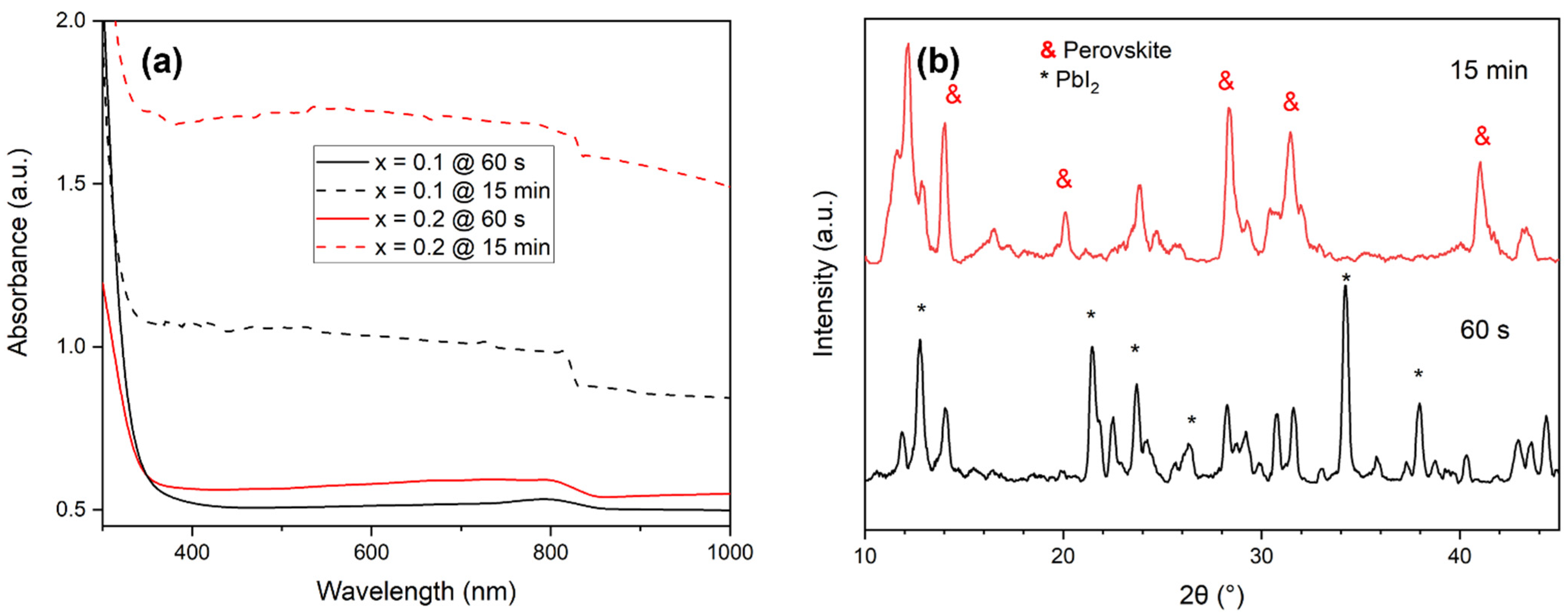
3.1. Effect of the Dipping Time
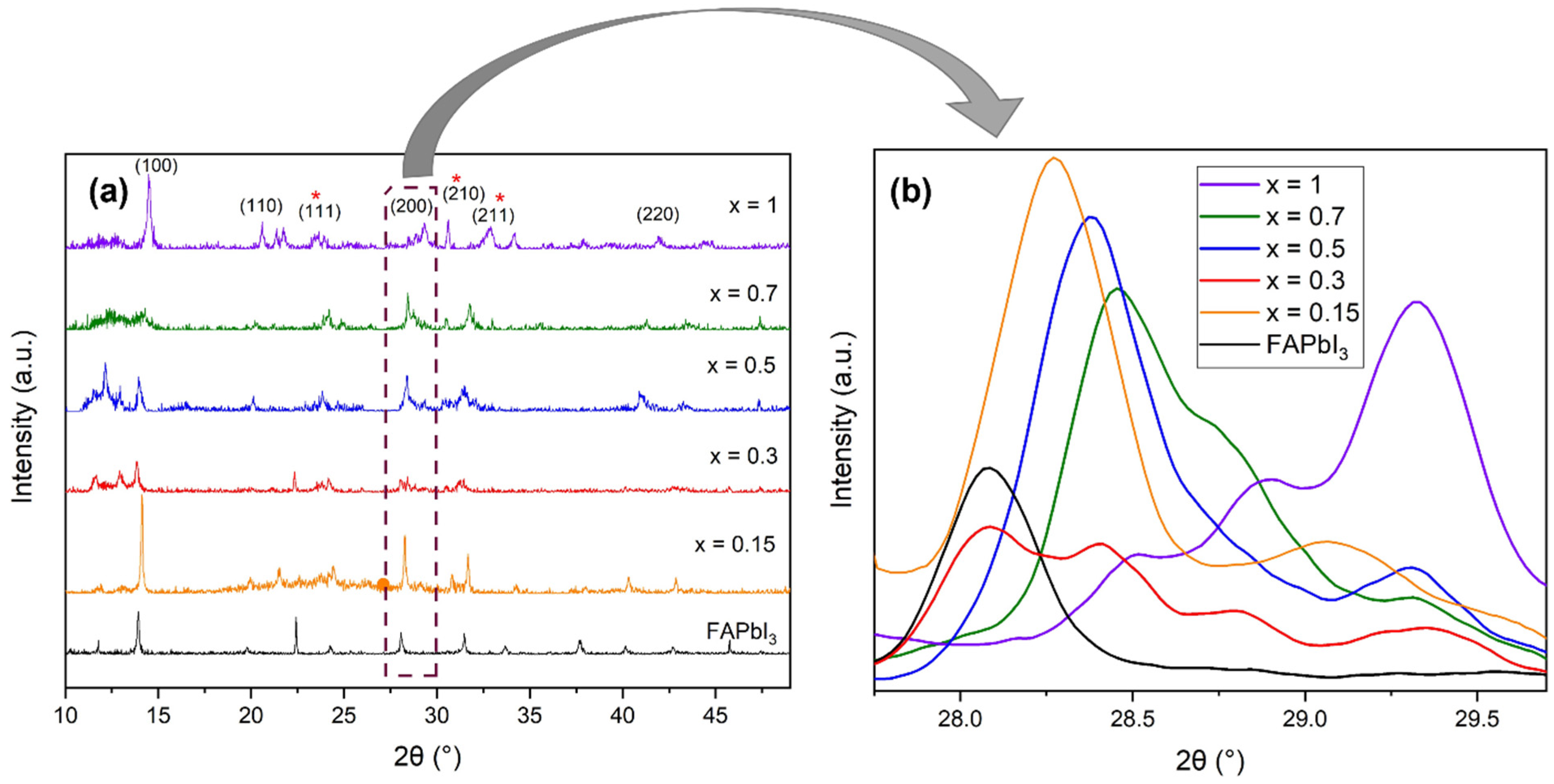
The dipping time of the PbI2 films in the CsBr, FAI and FABr solution was initially kept at 60 s because the literature on sequentially deposited MAPbI3 films suggested longer dipping times can cause poorer film coverage and lead to the formation of shunt pathways in the absorber layer [25]. However, experiments involving Br required a longer dipping time for complete conversion of the perovskite layer [23], so it was increased to 15 min. All other deposition parameters for the sequential deposition route were kept constant. According to the UV-Vis NIR spectroscopy results shown in Figure 1a, a longer dipping time resulted in a higher absorbance of the film. This can be attributed to a complete conversion of the perovskite and to an increased crystallinity, as highlighted in the XRD patterns of Figure 1b. The film dipped in the precursor solution for only 60 s shows a strong presence of PbI2 peaks, labeled with a black asterisk. The suppression of these peaks and the appearance of sharper perovskite phase peaks in the sample dipped for 15 min are a clear sign of a more crystalline perovskite structure with very little residual PbI2 [26]. The absorbance also enhanced with a distinct absorption edge as the CsBr content in the film was increased (Figure 1a) since the presence of Cs promotes the crystallization of the film [16] and enables the layer to absorb more light in the given wavelength range. It is worthwhile pointing out that the absorbance spectra of these films tend to be flat, which could be ascribable to their large crystal size and high thickness [27]. All the following samples were fabricated using a dipping time of 15 min.

3.2. XRD Analysis

The XRD patterns of the different film compositions are shown in Figure 2a. The characteristic perovskite peaks at around 14° (100), 20° (110), 28° (200) and 40° (220) were visible in all films. Their height increased and position shifted to higher angles as the Br content was gradually increased owing to lattice shrinkage. However, the PbI2 peak at ∼12° persisted throughout the different compositions, thus showing the presence of remnant PbI2 film. Another prominent phase in the Br-0.5, Br-0.7 and Br-1 films is visible at around 24° (111), 30° (210) and 34° (211). These values match with the CsPbBr3 perovskites, and it seems that the perovskite structure has a greater affinity for CsBr as compared to the FAI and FABr, which led to Cs-Br rich sites in the film. The ionic radius of Cs (179 pm) is smaller than that of FA (250 pm), which could be the reason why it is easily inserted into the structure. Mixed halide perovskites are likely to segregate into I-rich and Br-rich phases upon optical illumination as explained by the Hoke effect [28]. CsPbBr3 is also much more stable at room temperature and high moisture levels as compared to FA-based perovskites [29].
Figure 2b shows a magnification of the (200) XRD peak. The signal was processed, so the relative height of the peak does not depict the actual intensity. However, as it is visible from the graph, the peak shifted to a higher angle as the content of Br was increased, more specifically from 28.2° for FAPbI3 to 29.6° for FA0.8Cs0.2PbI3−xBrx with x = 1. This is characteristic of a shrinkage of the lattice and a reduction in crystal size. As more and more Br was added to the precursor, Iwas replaced. Since Br displays a smaller ionic radius (196 pm) than I- (220 pm), it causes the lattice to contract. These claims can be supported by what has already been reported in the literature [30,31]. Additionally, it is interesting to note that the relative intensity of absorbance increased as more Br was added to the precursor, which is a clear sign of a more ordered and crystalline perovskite phase [32].

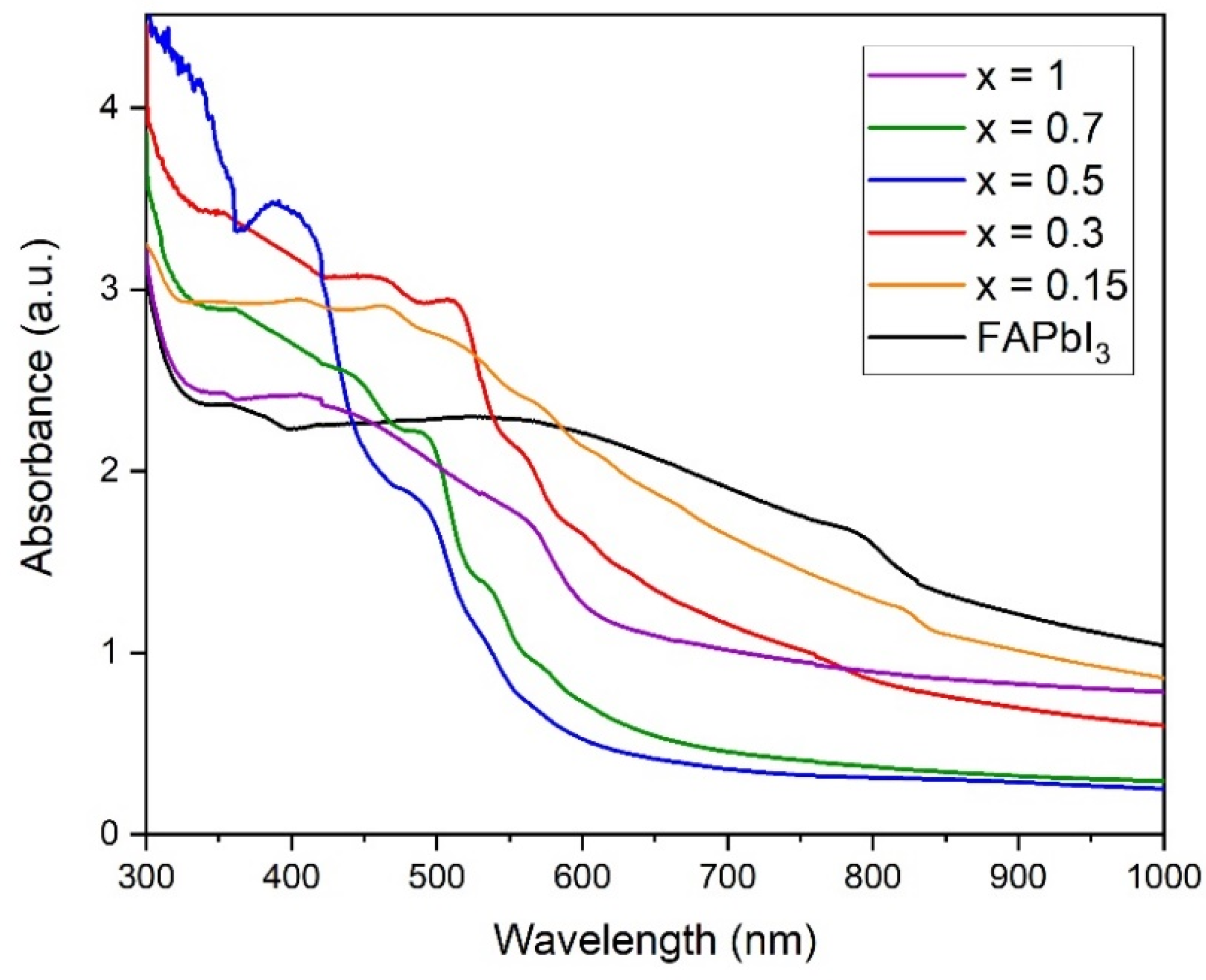
3.3. Optical Properties

To determine the bandgap and ascertain the optical behavior of the FA0.8Cs0.2PbI3−xBrx absorber layer films, UV-Vis NIR measurements in absorbance mode were performed (see Figure 3).
The absorbance graph of the FAPbI3 sample exhibits an absorption onset at around 830 nm, which corresponds to a bandgap of 1.49 eV in line with what reported in the literature [33]. A bandgap value of 1.52 eV was instead calculated through a Tauc plot using the thickness of 5 µm as obtained from the 2D optical profilometer. The same value was achieved for the sample with x = 0.15. The absorbance of the film with x = 0.3 is blue-shifted and a bandgap of 1.83 eV was assessed. However, as the percentage of Br was increased, the absorbance spectra are greatly blue-shifted. The bandgap increased to values higher than 2 eV for Br-0.5 and Br-0.7 films, which are closer to the 2.3 eV bandgap value reported in the literature for the CsPbBr3 [34]. In the absorbance graph, distinct absorption edges are also clearly visible at around 400–500 nm, which correspond to that present in the CsPbBr3 spectrum published by Atourki et al. [34]. This corroborates the presence of the CsPbBr3 peaks in the XRD patterns and proves that the FA cation was not included in the perovskite crystal structure of the films synthesized with a higher Br content. The CsBr salt results to be more dominant and the reason for this is the seven-times higher complexation constant between the Pb-Br species [35,36]. The higher affinity of Pb2+ towards Br ion led to the I ion playing the role of a spectator. The Br-1 film, however, displays a lower bandgap of 2 eV and the absorption onset is also red-shifted because a higher concentration of FABr was used to achieve this composition and therefore FA was included in the perovskite structure. Cs atoms accumulate in the grain boundaries when FABr is used [37]. There is an offset in the wavelength and a decrease in absorbance in the visible region as Br concentration increases due to the shrinkage of the crystal lattice leading to a lower optical density [27]. However, the absorbance of each film increased in the violet and ultraviolet range, i.e., 300–500 nm, which is ideal for wide bandgap materials. As inferred in the literature, the sharp increase in absorbance shows that the samples crystallinity enhances by adding more Br [16].
To study the correlation between the crystal size and the bandgap, while varying the Br content, they were plotted in the same graph (see Figure 4). This helped us to analyze the effect of Br addition on the structural properties of the perovskite absorber layers.
The crystal size of the different layers was calculated by analyzing the peaks from the XRD patterns. The peaks were fitted using a Gaussian distribution, and the full-width at half maximum (FWHM) was calculated. The size of the crystals was estimated using the Scherrer equation [38]:
B(2θ) = kλ/Lcos(θ),
where B is the FWHM, k the shape factor which is assumed to be 1 for simplicity, λ the X-ray wavelength, L the crystallite size in nm, and θ the peak angle in radians.
The crystallite size steadily decreased as the Br content was increased (see Figure 4) because of shrinkage of the crystal lattice due to increasing concentration of the smaller Br ion. It assumed a constant value, typical of CsPbBr3 phase, starting from x = 0.5. Conversely, the bandgap enhanced while increasing the Br content (see Figure 4), but interestingly it is much higher than the value reported in the literature due to the presence of the likely mixed CsPbBr3 phase [16]. The error bars indicate the maximum variation obtained from adjusting the Tauc plot tangent. Keeping the margin for error in mind, also the bandgap reached a plateau at a value which is close to that of CsPbBr3. The insets show that the color of the film also changed from black to red as the Br content was increased. This change in color indicates a phase shift as the composition becomes Br-rich [33].

3.4. Morphological Analyses

The SEM images of four different film compositions are reported in Figure 5.
The FA0.8Cs0.2PbI2.85Br0.15 sample shows smaller grains than the wide bandgap absorber layers reported in literature [15,39], but the film is compact with few visible voids. As the concentration of Br was increased, the x = 0.5 film displays a higher roughness and the emergence of more pinholes on the surface. For x = 0.7 sample, the grains become non-existent, and the film exhibits a very rough appearance. The coverage has somewhat improved but the structure is disordered, which was confirmed by the presence of multiple phases in the XRD pattern. For the x = 1 sample, larger grains are visible in the image, with an estimated average grain size of 500 nm. These bubble-like grains vary in size and have agglomerated together with some voids still present.
To investigate the roughness of the films and get an accurate idea of their topography, the samples were characterized using AFM and the obtained images are reported in Figure 6.
The FA0.8Cs0.2PbI2.85Br0.15 (x = 0.15) sample exhibits an average roughness of 68.7 nm, which was calculated by edge detection. For the x = 0.5 sample the value increased to 110 nm. Further increasing of the Br content led to the enhancement of the roughness from 153 nm for x = 0.7 to 234 nm for x = 1, as it is evident by the non-homogenous topography. The AFM images show that the roughness increased while increasing the Br content of the film. A rougher absorber layer helps in trapping more light and reducing reflectance losses [23], but it may also negatively affect the device performance due to the presence of voids.

4. Conclusions

In conclusion, the optical, morphological and structural properties of mixed cation and mixed halide wide bandgap perovskite absorber layers fabricated through sequential deposition technique were thoroughly investigated. The composition was tuned by keeping the FA and Cs ratio constant while varying the Br and I ratio. The samples exhibited a perovskite crystal structure and the crystallinity of the layer improved as the Br concentration was increased up to x ≤ 0.3 for FA0.8Cs0.2PbI3−xBrx as confirmed by both UV-Visible NIR spectroscopy and XRD analysis results. As the Br concentration was increased, a CsPbBr3 perovskite phase emerged because the Br ion is favored over the I ion by the Pb atom. The absorbance of the films in the 300–500 nm range enhanced by increasing the Br content, which is encouraging for wide bandgap applications. The bandgap increased from 1.52 eV for the FAPbI3 film up to 1.83 eV for FA0.8Cs0.2PbI2.7Br0.3; however, further increase in the CsBr salt led to a drastic blue-shift in the absorption onset confirming the presence of CsPbBr3. The constant value assumed by the bandgap and crystallite size for x ≥ 0.5 was also characteristic of the CsPbBr3 perovskite. The sequential spin coating/dip coating deposition method reported in this research revealed to be an effective strategy for fabricating wide bandgap perovskite absorber layers. The evaluation of the photovoltaic performance of the synthesized films up to x = 0.3 in wide bandgap PSCs will be the object of a future study.

Author Contributions

Conceptualization, methodology, writing—original draft preparation, M.A.; investigation and validation, M.A., M.A.T. and A.S.; writing—review and editing, M.A., N.S. and D.P.; supervision, N.S. All authors have read and agreed to the published version of the manuscript.

Funding

This research was funded by HIGHER EDUCATION COMMISSION, PAKISTAN, grant number NRPU-6046.

Institutional Review Board Statement

Not applicable.

Informed Consent Statement

Informed consent was obtained from all subjects involved in the study.

Data Availability Statement

Data available on request due to restrictions of privacy.

Acknowledgments

The authors would like to thank Micaela Castellino of Politecnico di Torino for her valuable guidance.

Conflicts of Interest

The authors declare no conflict of interest. The funders had no role in the design of the study; in the collection, analyses, or interpretation of data; in the writing of the manuscript, or in the decision to publish the results.

References

  1. Yin, W.-J.; Yang, J.-H.; Kang, J.; Yan, Y.; Wei, S.-H. Halide Perovskite Materials for Solar Cells: A Theoretical Review. J. Mater. Chem. A 2015, 3, 8926–8942. [Google Scholar] [CrossRef]
  2. Hwang, K.; Jung, Y.-S.; Heo, Y.-J.; Scholes, F.H.; Watkins, S.E.; Subbiah, J.; Jones, D.J.; Kim, D.-Y.; Vak, D. Toward Large Scale Roll-to-Roll Production of Fully Printed Perovskite Solar Cells. Adv. Mater. 2015, 27, 1241–1247. [Google Scholar] [CrossRef]
  3. Lin, R.; Xiao, K.; Qin, Z.; Han, Q.; Zhang, C.; Wei, M.; Saidaminov, M.I.; Gao, Y.; Xu, J.; Xiao, M.; et al. Monolithic All-Perovskite Tandem Solar Cells with 24.8% Efficiency Exploiting Comproportionation to Suppress Sn(ii) Oxidation in Precursor Ink. Nat. Energy 2019, 4, 864–873. [Google Scholar] [CrossRef]
  4. Hou, Y.; Aydin, E.; de Bastiani, M.; Xiao, C.; Isikgor, F.H.; Xue, D.-J.; Chen, B.; Chen, H.; Bahrami, B.; Chowdhury, A.H.; et al. Efficient Tandem Solar Cells with Solution-Processed Perovskite on Textured Crystalline Silicon. Science 2020, 367, 1135–1140. [Google Scholar] [CrossRef]
  5. Chen, B.; Yu, Z.J.; Manzoor, S.; Wang, S.; Weigand, W.; Yu, Z.; Yang, G.; Ni, Z.; Dai, X.; Holman, Z.C.; et al. Blade-Coated Perovskites on Textured Silicon for 26%-Efficient Monolithic Perovskite/Silicon Tandem Solar Cells. Joule 2020, 4, 850–864. [Google Scholar] [CrossRef]
  6. Al-Ashouri, A.; Köhnen, E.; Li, B.; Magomedov, A.; Hempel, H.; Caprioglio, P.; Márquez, J.A.; Vilches, A.B.M.; Kasparavicius, E.; Smith, J.A.; et al. Monolithic Perovskite/Silicon Tandem Solar Cell with >29% Efficiency by Enhanced Hole Extraction. Science 2020, 370, 1300–1309. [Google Scholar] [CrossRef] [PubMed]
  7. Photovoltaic Research NREL. Best Research-Cell Efficiency Chart. Available online: https://www.nrel.gov/pv/cell-efficiency.html (accessed on 15 May 2021).
  8. Kieslich, G.; Sun, S.; Cheetham, A.K. An Extended Tolerance Factor Approach for Organic-Inorganic Perovskites. Chem. Sci. 2015, 6, 3430–3433. [Google Scholar] [CrossRef] [PubMed] [Green Version]
  9. Saliba, M.; Correa-Baena, J.-P.; Grätzel, M.; Hagfeldt, A.; Abate, A. Perovskite Solar Cells: From the Atomic Level to Film Quality and Device Performance. Angew. Chem. Int. Ed. 2018, 57, 2554–2569. [Google Scholar] [CrossRef] [PubMed]
  10. Hörantner, M.T.; Leijtens, T.; Ziffer, M.E.; Eperon, G.E.; Christoforo, M.G.; McGehee, M.D.; Snaith, H.J. The Potential of Multijunction Perovskite Solar Cells. ACS Energy Lett. 2017, 2, 2506–2513. [Google Scholar] [CrossRef]
  11. Song, Z.; Chen, C.; Li, C.; Awni, R.A.; Zhao, D.; Yan, Y. Wide-Bandgap, Low-Bandgap, and Tandem Perovskite Solar Cells. Semicond. Sci. Technol. 2019, 34, 093001. [Google Scholar] [CrossRef]
  12. Zhang, X.; Liu, J.; Song, Z.; Zuo, W.; Fan, Z.; He, X.; Luo, K.; Ye, Q.; Liao, C. Tuning Bandgap of Mixed-Halide Perovskite for Improved Photovoltaic Performance Under Monochromatic-Light Illumination. Phys. Status Solidi (A) Appl. Mater. Sci. 2019, 216, 1800727. [Google Scholar] [CrossRef]
  13. Kot, M.; Vorokhta, M.; Wang, Z.; Snaith, H.J.; Schmeißer, D.; Flege, J.I. Thermal Stability of CH3NH3PbIxCl3−x versus [HC(NH2)2]0.83Cs0.17PbI2.7Br0.3 Perovskite Films by X-Ray Photoelectron Spectroscopy. Appl. Surf. Sci. 2020, 513, 145596. [Google Scholar] [CrossRef]
  14. Szostak, R.; Marchezi, P.E.; Marques, A.D.S.; da Silva, J.C.; de Holanda, M.S.; Soares, M.M.; Tolentino, H.C.N.; Nogueira, A.F. Exploring the Formation of Formamidinium-Based Hybrid Perovskites by Antisolvent Methods: In Situ GIWAXS Measurements during Spin Coating. Sustain. Energy Fuels 2019, 3, 2287–2297. [Google Scholar] [CrossRef]
  15. Zhou, Y.; Jia, Y.-H.; Fang, H.-H.; Loi, M.A.; Xie, F.-Y.; Gong, L.; Qin, M.-C.; Lu, X.-H.; Wong, C.-P.; Zhao, N. Composition-Tuned Wide Bandgap Perovskites: From Grain Engineering to Stability and Performance Improvement. Adv. Funct. Mater. 2018, 28, 1803130. [Google Scholar] [CrossRef]
  16. McMeekin, D.P.; Sadoughi, G.; Rehman, W.; Eperon, G.E.; Saliba, M.; Hörantner, M.T.; Haghighirad, A.; Sakai, N.; Korte, L.; Rech, B.; et al. A Mixed-Cation Lead Mixed-Halide Perovskite Absorber for Tandem Solar Cells. Science 2016, 351, 151–155. [Google Scholar] [CrossRef] [PubMed] [Green Version]
  17. Lin, Y.; Chen, B.; Zhao, F.; Zheng, X.; Deng, Y.; Shao, Y.; Fang, Y.; Bai, Y.; Wang, C.; Huang, J. Matching Charge Extraction Contact for Wide-Bandgap Perovskite Solar Cells. Adv. Mater. 2017, 29, 1700607. [Google Scholar] [CrossRef] [PubMed]
  18. Zhao, Y.; Liu, J.; Lu, X.; Gao, Y.; You, X.; Xu, X. Improving the Efficiency of Perovskite Solar Cells through Optimization of the CH3NH3PbI3 Film Growth in Solution Process Method. Appl. Surf. Sci. 2015, 359, 560–566. [Google Scholar] [CrossRef]
  19. Zheng, L.; Ma, Y.; Chu, S.; Wang, S.; Qu, B.; Xiao, L.; Chen, Z.; Gong, Q.; Wu, Z.; Hou, X. Improved Light Absorption and Charge Transport for Perovskite Solar Cells with Rough Interfaces by Sequential Deposition. Nanoscale 2014, 6, 8171–8176. [Google Scholar] [CrossRef] [PubMed]
  20. Burschka, J.; Pellet, N.; Moon, S.-J.; Humphry-Baker, R.; Gao, P.; Nazeeruddin, M.K.; Grätzel, M. Sequential Deposition as a Route to High-Performance Perovskite-Sensitized Solar Cells. Nature 2013, 499, 316–319. [Google Scholar] [CrossRef] [PubMed]
  21. Xie, Y.; Shao, F.; Wang, Y.; Xu, T.; Wang, D.; Huang, F. Enhanced Performance of Perovskite CH3NH3PbI3 Solar Cell by Using CH3NH3I as Additive in Sequential Deposition. ACS Appl. Mater. Interfaces 2015, 7, 12937–12942. [Google Scholar] [CrossRef]
  22. Koh, T.M.; Fu, K.; Fang, Y.; Chen, S.; Sum, T.C.; Mathews, N.; Mhaisalkar, S.G.; Boix, P.P.; Baikie, T. Formamidinium-Containing Metal-Halide: An Alternative Material for Near-IR Absorption Perovskite Solar Cells. J. Phys. Chem. C 2014, 118, 16458–16462. [Google Scholar] [CrossRef]
  23. Kulkarni, S.A.; Baikie, T.; Boix, P.P.; Yantara, N.; Mathews, N.; Mhaisalkar, S. Band-Gap Tuning of Lead Halide Perovskites Using a Sequential Deposition Process. J. Mater. Chem. A 2014, 2, 9221–9225. [Google Scholar] [CrossRef] [Green Version]
  24. Koh, T.M.; Krishnamoorthy, T.; Yantara, N.; Shi, C.; Leong, W.L.; Boix, P.P.; Grimsdale, A.C.; Mhaisalkar, S.G.; Mathews, N. Formamidinium Tin-Based Perovskite with Low Eg for Photovoltaic Applications. J. Mater. Chem. A 2015, 3, 14996–15000. [Google Scholar] [CrossRef]
  25. Ahmadian-Yazdi, M.R.; Zabihi, F.; Habibi, M.; Eslamian, M. Effects of Process Parameters on the Characteristics of Mixed-Halide Perovskite Solar Cells Fabricated by One-Step and Two-Step Sequential Coating. Nanoscale Res. Lett. 2016, 11, 408. [Google Scholar] [CrossRef] [PubMed] [Green Version]
  26. Liang, K.; Mitzi, D.B.; Prikas, M.T. Synthesis and Characterization of Organic-Inorganic Perovskite Thin Films Prepared Using a Versatile Two-Step Dipping Technique. Chem. Mater. 1998, 10, 403–411. [Google Scholar] [CrossRef]
  27. Tian, Y.; Scheblykin, I.G. Artifacts in Absorption Measurements of Organometal Halide Perovskite Materials: What Are the Real Spectra? J. Phys. Chem. Lett. 2015, 6, 3466–3470. [Google Scholar] [CrossRef] [PubMed] [Green Version]
  28. Brennan, M.C.; Draguta, S.; Kamat, P.V.; Kuno, M. Light-Induced Anion Phase Segregation in Mixed Halide Perovskites. ACS Energy Lett. 2018, 3, 204–213. [Google Scholar] [CrossRef] [Green Version]
  29. Kulbak, M.; Cahen, D.; Hodes, G. How Important Is the Organic Part of Lead Halide Perovskite Photovoltaic Cells? Efficient CsPbBr3 Cells. J. Phys. Chem. Lett. 2015, 6, 2452–2456. [Google Scholar] [CrossRef]
  30. Atourki, L.; Vega, E.; Marí, B.; Mollar, M.; Ait Ahsaine, H.; Bouabid, K.; Ihlal, A. Role of the Chemical Substitution on the Structural and Luminescence Properties of the Mixed Halide Perovskite Thin MAPbI3−xBrx (0 ≤ x ≤ 1) Films. Appl. Surf. Sci. 2016, 371, 112–117. [Google Scholar] [CrossRef]
  31. Pengpad, A.; Ruankham, P.; Rattanachata, A.; Rattanasuporn, S.; Jenpiyapong, W.; Nakajima, H.; Choopun, S.; Amornkitbamrung, V. Surface Composition of MAPb(IxBr1−x)3 (0 ≤ x ≤ 1) Organic-Inorganic Mixed-Halide Perovskites. Appl. Surf. Sci. 2019, 479, 311–317. [Google Scholar] [CrossRef]
  32. Huang, J.; Yuan, Y.; Shao, Y.; Yan, Y. Understanding the Physical Properties of Hybrid Perovskites for Photovoltaic Applications. Nat. Rev. Mater. 2017, 2, 17042. [Google Scholar] [CrossRef]
  33. Eperon, G.E.; Stranks, S.D.; Menelaou, C.; Johnston, M.B.; Herz, L.M.; Snaith, H.J. Formamidinium Lead Trihalide: A Broadly Tunable Perovskite for Efficient Planar Heterojunction Solar Cells. Energy Environ. Sci. 2014, 7, 982–988. [Google Scholar] [CrossRef]
  34. Atourki, L.; Vega, E.; Mollar, M.; Marí, B.; Kirou, H.; Bouabid, K.; Ihlal, A. Impact of Iodide Substitution on the Physical Properties and Stability of Cesium Lead Halide Perovskite Thin Films CsPbBr3−xIx (0 ≤ x ≤ 1). J. Alloys Compd. 2017, 702, 404–409. [Google Scholar] [CrossRef]
  35. Yoon, S.J.; Kuno, M.; Kamat, P.V. Shift Happens. How Halide Ion Defects Influence Photoinduced Segregation in Mixed Halide Perovskites. ACS Energy Lett. 2017, 2, 1507–1514. [Google Scholar] [CrossRef] [Green Version]
  36. Yoon, S.J.; Stamplecoskie, K.G.; Kamat, P.V. How Lead Halide Complex Chemistry Dictates the Composition of Mixed Halide Perovskites. J. Phys. Chem. Lett. 2016, 7, 1368–1373. [Google Scholar] [CrossRef] [PubMed]
  37. Svanström, S.; Jacobsson, T.J.; Sloboda, T.; Giangrisostomi, E.; Ovsyannikov, R.; Rensmo, H.; Cappel, U.B. Effect of Halide Ratio and Cs+ Addition on the Photochemical Stability of Lead Halide Perovskites. J. Mater. Chem. A 2018, 6, 22134–22144. [Google Scholar] [CrossRef] [Green Version]
  38. Patterson, A.L. The Scherrer Formula for X-Ray Particle Size Determination. Phys. Rev. 1939, 56, 978–982. [Google Scholar] [CrossRef]
  39. Tan, H.; Che, F.; Wei, M.; Zhao, Y.; Saidaminov, M.I.; Todorović, P.; Broberg, D.; Walters, G.; Tan, F.; Zhuang, T.; et al. Dipolar Cations Confer Defect Tolerance in Wide-Bandgap Metal Halide Perovskites. Nat. Commun. 2018, 9, 3100. [Google Scholar] [CrossRef] [PubMed]
Figure 1. (a) Absorbance spectra of the FA0.8Cs0.2PbI3−xBrx perovskite layers, where x represents the molar ratio of Br. (b) XRD patterns of Br-0.2 after increasing the dipping time from 60 s up to 15 min. The red ampersand denotes the perovskite peaks, while the black asterisk is a label for PbI2 peaks.
Energies 14 08401 g001
Figure 2. (a) XRD patterns of the FAPbI3 and FA0.8Cs0.2PbI3−xBrx perovskite layers labeled by the concentration of Br used. The red asterisk corresponds to the CsPbBr3 peaks. (b) Zoom-up of the XRD patterns in correspondence of the (200) peak.
Energies 14 08401 g002
Figure 3. Absorbance spectra of the FAPbI3 and FA0.8Cs0.2PbI3−xBrx perovskite layers.
Energies 14 08401 g003
Figure 4. Relationship between the Br concentration, bandgap and crystal size of the FA0.8Cs0.2PbI3−xBrx perovskites. The insets show top-view photographs of the 1 × 1 cm2 films taken after deposition and the red bars represent the error for the bandgap.
Energies 14 08401 g004
Figure 5. SEM images of (a) FA0.8Cs0.2PbI2.85Br0.15, (b) FA0.8Cs0.2PbI2.5Br0.5, (c) FA0.8Cs0.2PbI2.3Br0.7, and (d) FA0.8Cs0.2PbI2Br1 films deposited on FTO-coated glass substrates.
Energies 14 08401 g005
Figure 6. AFM 3D topography images of (a) FA0.8Cs0.2PbI2.85Br0.15, (b) FA0.8Cs0.2PbI2.5Br0.5, (c) FA0.8Cs0.2PbI2.3Br0.7, and (d) FA0.8Cs0.2PbI2Br1 films deposited on FTO-covered glass substrates.
Energies 14 08401 g006
Publisher’s Note: MDPI stays neutral with regard to jurisdictional claims in published maps and institutional affiliations.

