
Charge Transporting Materials Grown by Atomic Layer Deposition in Perovskite Solar Cells


Abstract
:1. Introduction
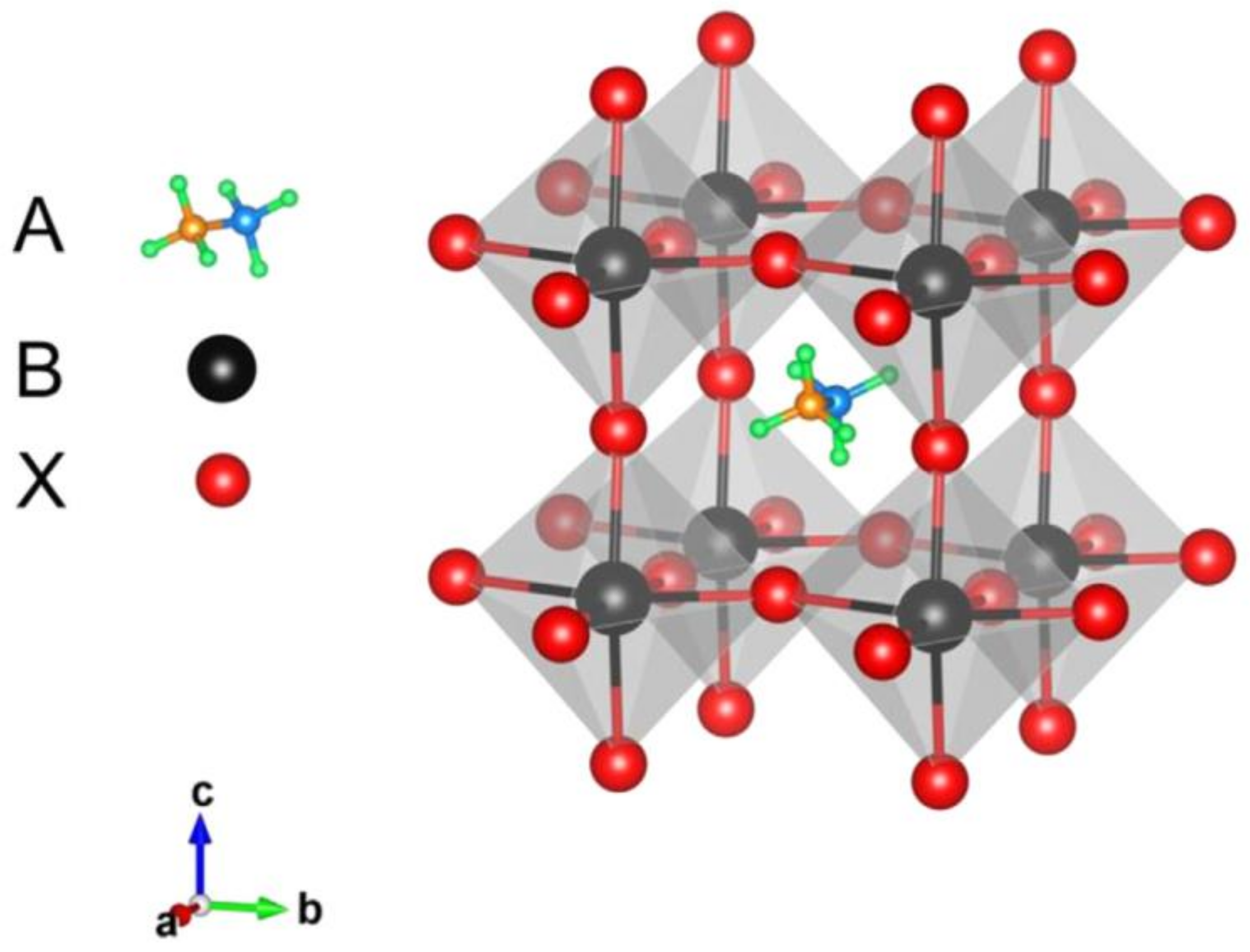
2. Perovskite Solar Cells
3. Atomic Layer Deposition (ALD)
4. Charge Transporting Materials (CTM) Grown by ALD
4.1. Electron Transporting Materials
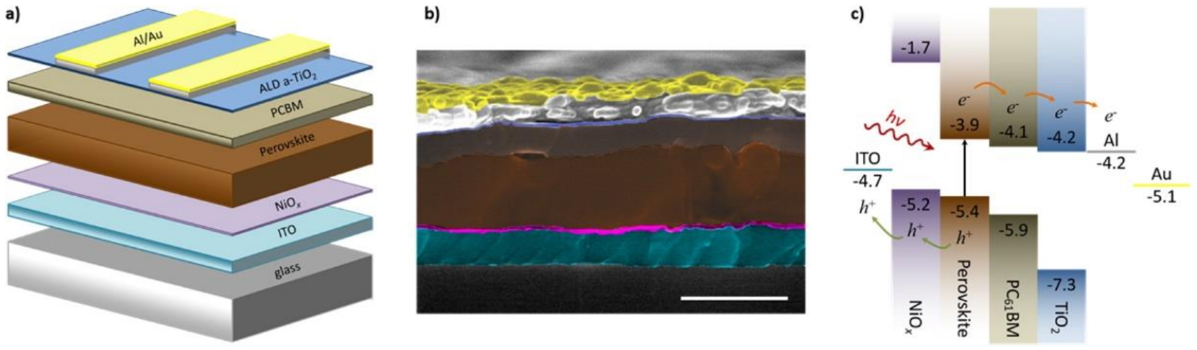
4.1.1. TiOx
4.1.2. ZnO
4.1.3. Nb2O5
4.1.4. SnOx
4.2. Hole Transporting Materials
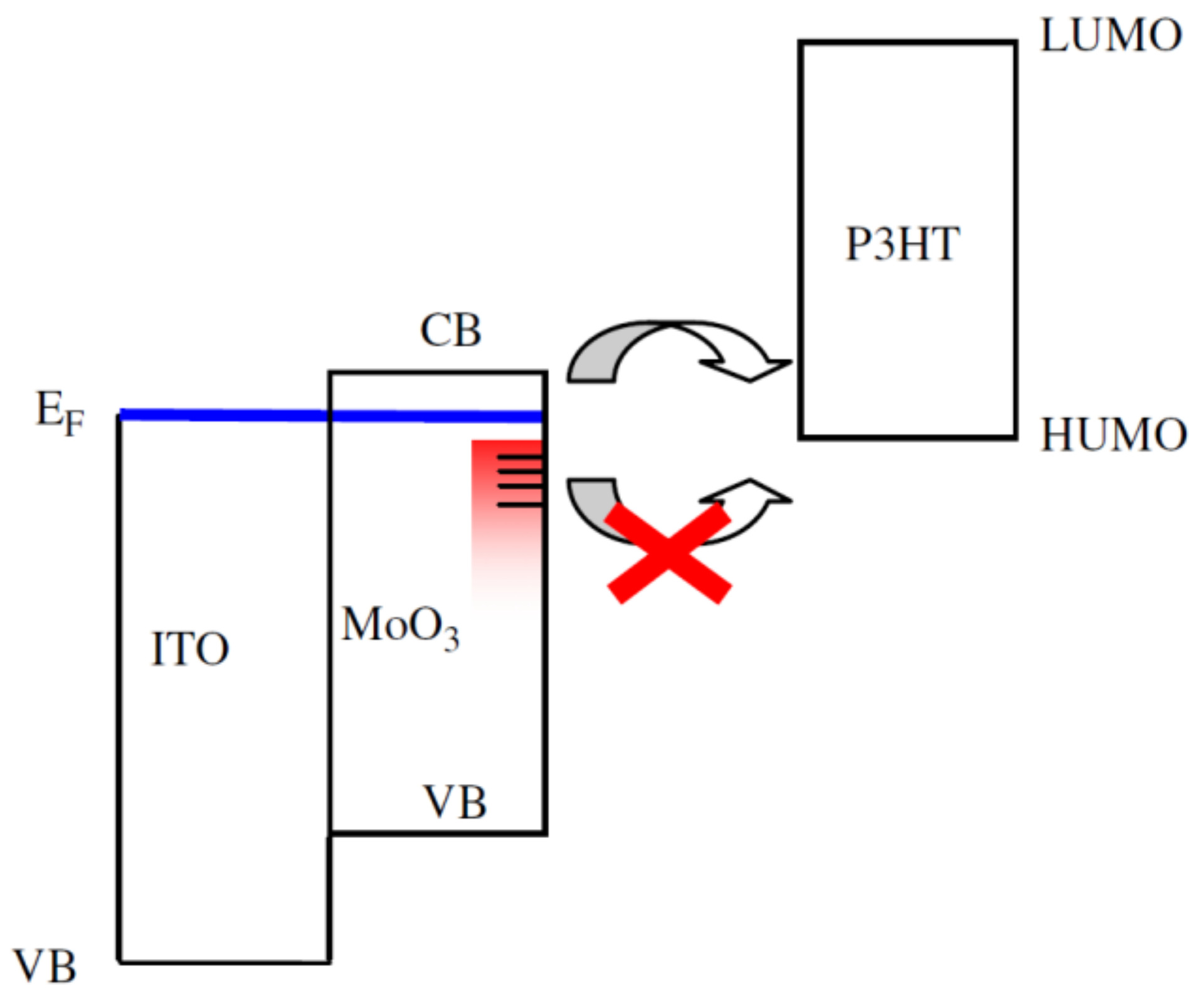
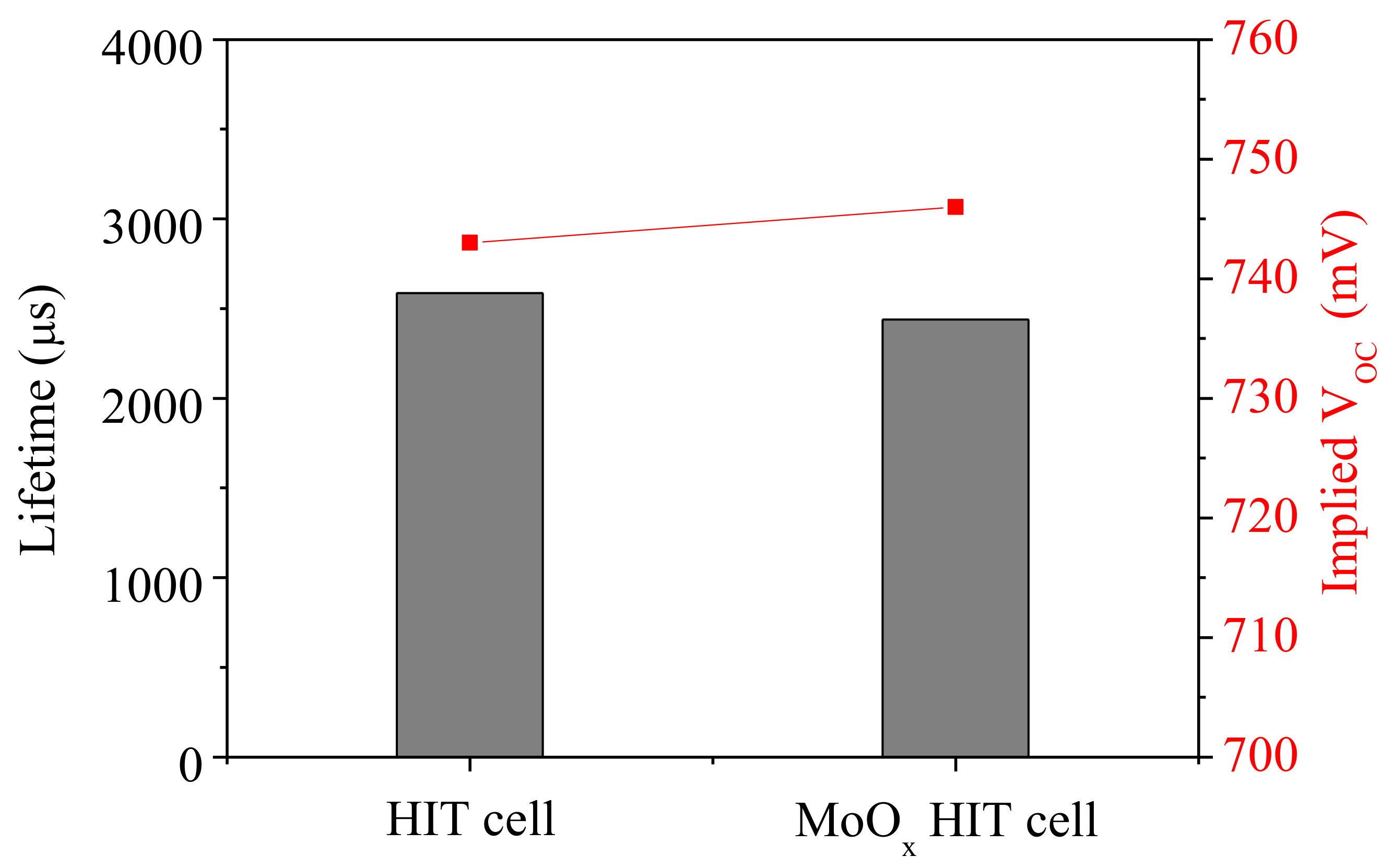
4.2.1. MoOX
4.2.2. WOx
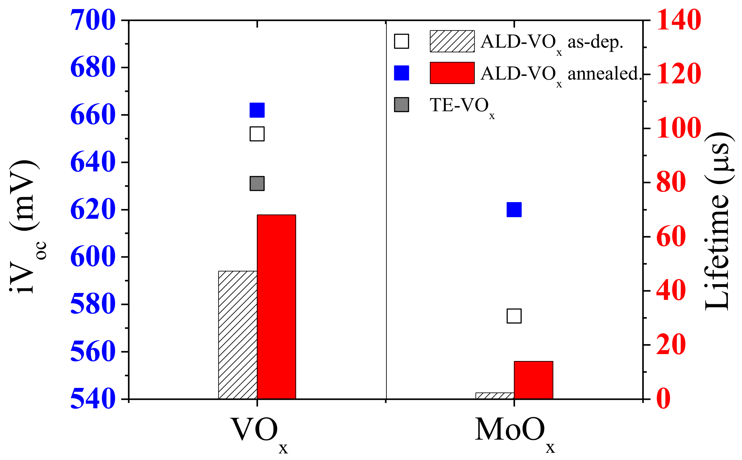
4.2.3. VOX
4.2.4. NiOx
5. Conclusions and Perspectives
Author Contributions
Funding
Institutional Review Board Statement
Informed Consent Statement
Data Availability Statement
Acknowledgments
Conflicts of Interest
References
- NREL. Best Research Efficiency. Available online: https://www.nrel.gov/pv/assets/pdfs/best-research-cell-efficiencies.20210104.pdf (accessed on 14 February 2020).
- Roesch, R.; Faber, T.; Von Hauff, E.; Brown, T.M.; Lira-Cantu, M.; Hoppe, H. Procedures and practices for evaluating thin-film solar cell stability. Adv. Energy Mater. 2015, 5, 1501407. [Google Scholar] [CrossRef] [Green Version]
- Niu, G.; Guo, X.; Wang, L. Review of recent progress in chemical stability of perovskite solar cells. J. Mater. Chem. A 2015, 3, 8970–8980. [Google Scholar] [CrossRef]
- Pathak, S.K.; Abate, A.; Ruckdeschel, P.; Roose, B.; Gödel, K.C.; Vaynzof, Y.; Santhala, A.; Watanabe, S.-I.; Hollman, D.J.; Noel, N.; et al. Performance and Stability Enhancement of Dye-Sensitized and Perovskite Solar Cells by Al Doping of TiO2. Adv. Funct. Mater. 2014, 24, 6046–6055. [Google Scholar] [CrossRef]
- Grätzel, M. The light and shade of perovskite solar cells. Nat. Mater. 2014, 13, 838–842. [Google Scholar] [CrossRef]
- Calió, L.; Kazim, S.; Grätzel, M.; Ahmad, S. Hole-Transport Materials for Perovskite Solar Cells. Angew. Chem. Int. Ed. 2016, 55, 14522–14545. [Google Scholar] [CrossRef]
- Wang, D.; Wright, M.; Elumalai, N.K.; Uddin, A. Stability of perovskite solar cells. Sol. Energy Mater. Sol. Cells 2016, 147, 255–275. [Google Scholar] [CrossRef]
- Zuo, C.; Bolink, H.J.; Han, H.; Huang, J.; Cahen, D.; Ding, L. Advances in Perovskite Solar Cells. Adv. Sci. 2016, 3, 1500324. [Google Scholar] [CrossRef]
- Wehrenfennig, C.; Eperon, G.E.; Johnston, M.B.; Snaith, H.J.; Herz, L.M. High Charge Carrier Mobilities and Lifetimes in Organolead Trihalide Perovskites. Adv. Mater. 2014, 26, 1584–1589. [Google Scholar] [CrossRef] [Green Version]
- Weber, D. CH3NH3PbX3, ein Pb(II)-System mit kubischer Perowskitstruktur / CH3NH3PbX3, a Pb(II)-System with Cubic Perovskite Structure. Z. Naturforsch. B 1978, 33, 1443–1445. [Google Scholar] [CrossRef]
- Mitzi, D.B.; Feild, C.A.; Harrison, W.T.A.; Guloy, A.M. Conducting tin halides with a layered organic-based perovskite structure. Nature 1994, 369, 467–469. [Google Scholar] [CrossRef]
- Green, M.A.; Ho-Baillie, A. Perovskite Solar Cells: The Birth of a New Era in Photovoltaics. ACS Energy Lett. 2017, 2, 822–830. [Google Scholar] [CrossRef]
- Im, J.-H.; Lee, C.-R.; Lee, J.-W.; Park, S.-W.; Park, N.-G. 6.5% efficient perovskite quantum-dot-sensitized solar cell. Nanoscale 2011, 3, 4088. [Google Scholar] [CrossRef] [Green Version]
- Kim, H.-S.; Lee, C.-R.; Im, J.-H.; Lee, K.-B.; Moehl, T.; Marchioro, A.; Moon, S.-J.; Humphry-Baker, R.; Yum, J.-H.; Moser, J.E.; et al. Lead Iodide Perovskite Sensitized All-Solid-State Submicron Thin Film Mesoscopic Solar Cell with Efficiency Exceeding 9%. Sci. Rep. 2012, 2, 591. [Google Scholar] [CrossRef] [Green Version]
- Zhang, W.; Wang, Y.-C.; Li, X.; Song, C.; Wan, L.; Usman, K.; Fang, J. Recent Advance in Solution-Processed Organic Interlayers for High-Performance Planar Perovskite Solar Cells. Adv. Sci. 2018, 5, 1800159. [Google Scholar] [CrossRef]
- Wang, K.; Olthof, S.; Subhani, W.S.; Jiang, X.; Cao, Y.; Duan, L.; Wang, H.; Du, M.; Liu, S. (Frank) Novel inorganic electron transport layers for planar perovskite solar cells: Progress and prospective. Nano Energy 2020, 68, 104289. [Google Scholar] [CrossRef]
- Qin, P.; Tanaka, S.; Ito, S.; Tetreault, N.; Manabe, K.; Nishino, H.; Nazeeruddin, M.K.; Grätzel, M. Inorganic hole conductor-based lead halide perovskite solar cells with 12.4% conversion efficiency. Nat. Commun. 2014, 5, 3834. [Google Scholar] [CrossRef] [Green Version]
- An, K.S.; Cho, W.; Sung, K.; Lee, S.S.; Kim, Y. Preparation of Al2O3 Thin Films by Atomic Layer Deposition Using Dimethylaluminum Isopropoxide and Water and Their Reaction Mechanisms. Bull. Korean Chem. Soc. 2003, 24, 1659–1663. [Google Scholar] [CrossRef] [Green Version]
- Benick, J.; Hoex, B.; van de Sanden, M.C.M.; Kessels, W.M.M.; Schultz, O.; Glunz, S.W. High efficiency n-type Si solar cells on Al2O3-passivated boron emitters. Appl. Phys. Lett. 2008, 92, 253504. [Google Scholar] [CrossRef] [Green Version]
- Kim, I.S.; Cao, D.H.; Buchholz, D.B.; Emery, J.D.; Farha, O.K.; Hupp, J.T.; Kanatzidis, M.G.; Martinson, A.B.F. Liquid Water- and Heat-Resistant Hybrid Perovskite Photovoltaics via an Inverted ALD Oxide Electron Extraction Layer Design. Nano Lett. 2016, 16, 7786–7790. [Google Scholar] [CrossRef]
- Chiam, S.Y.; Dasgupta, B.; Soler, D.; Leung, M.Y.; Liu, H.; Ooi, Z.E.; Wong, L.M.; Jiang, C.Y.; Chang, K.L.; Zhang, J. Investigating the stability of defects in MoO3 and its role in organic solar cells. Sol. Energy Mater. Sol. Cells 2012, 99, 197–203. [Google Scholar] [CrossRef]
- Lu, H.; Tian, W.; Gu, B.; Zhu, Y.; Li, L. TiO2 Electron Transport Bilayer for Highly Efficient Planar Perovskite Solar Cell. Small 2017, 13, 1701535. [Google Scholar] [CrossRef]
- Kim, B.J.; Kim, D.H.; Lee, Y.-Y.; Shin, H.-W.; Han, G.S.; Hong, J.S.; Mahmood, K.; Ahn, T.K.; Joo, Y.-C.; Hong, K.S.; et al. Highly efficient and bending durable perovskite solar cells: Toward a wearable power source. Energy Environ. Sci. 2015, 8, 916–921. [Google Scholar] [CrossRef]
- Yang, G.; Lei, H.; Tao, H.; Zheng, X.; Ma, J.; Liu, Q.; Ke, W.; Chen, Z.; Xiong, L.; Qin, P.; et al. Reducing Hysteresis and Enhancing Performance of Perovskite Solar Cells Using Low-Temperature Processed Y-Doped SnO2 Nanosheets as Electron Selective Layers. Small 2017, 13, 1601769. [Google Scholar] [CrossRef]
- Mahmood, K.; Sarwar, S.; Mehran, M.T. Current status of electron transport layers in perovskite solar cells: Materials and properties. RSC Adv. 2017, 7, 17044–17062. [Google Scholar] [CrossRef] [Green Version]
- Yang, G.; Tao, H.; Qin, P.; Ke, W.; Fang, G. Recent progress in electron transport layers for efficient perovskite solar cells. J. Mater. Chem. A 2016, 4, 3970–3990. [Google Scholar] [CrossRef]
- Subbiah, A.S.; Dhara, A.K.; Mahuli, N.; Banerjee, S.; Sarkar, S.K. Ultra-Thin Atomic Layer Deposited–Nb2O5 as Electron Transport Layer for Co-Evaporated MAPbI 3 Planar Perovskite Solar Cells. Energy Technol. 2020, 8, 1900878. [Google Scholar] [CrossRef]
- Zhu, Y.; Deng, K.; Sun, H.; Gu, B.; Lu, H.; Cao, F.; Xiong, J.; Li, L. TiO2 Phase Junction Electron Transport Layer Boosts Efficiency of Planar Perovskite Solar Cells. Adv. Sci. 2018, 5, 1700614. [Google Scholar] [CrossRef] [Green Version]
- Zeng, T.; Su, X.; Feng, S.; Xie, Y.; Chen, Y.; Shen, Z.; Shi, W. Thermally-stable hydroxyl radicals implanted on TiO2 electron transport layer for efficient carrier extraction in PbS quantum dot photovoltaics. Sol. Energy Mater. Sol. Cells 2018, 188, 263–272. [Google Scholar] [CrossRef]
- Chang, C.-Y.; Lee, K.-T.; Huang, W.-K.; Siao, H.-Y.; Chang, Y.-C. High-Performance, Air-Stable, Low-Temperature Processed Semitransparent Perovskite Solar Cells Enabled by Atomic Layer Deposition. Chem. Mater. 2015, 27, 5122–5130. [Google Scholar] [CrossRef]
- Wali, Q.; Iqbal, Y.; Pal, B.; Lowe, A.; Jose, R. Tin oxide as an emerging electron transport medium in perovskite solar cells. Sol. Energy Mater. Sol. Cells 2018, 179, 102–117. [Google Scholar] [CrossRef]
- Yang, J.; Siempelkamp, B.D.; Mosconi, E.; De Angelis, F.; Kelly, T.L. Origin of the Thermal Instability in CH3NH3PbI3 Thin Films Deposited on ZnO. Chem. Mater. 2015, 27, 4229–4236. [Google Scholar] [CrossRef]
- Hultqvist, A.; Aitola, K.; Sveinbjörnsson, K.; Saki, Z.; Larsson, F.; Törndahl, T.; Johansson, E.; Boschloo, G.; Edoff, M. Atomic Layer Deposition of Electron Selective SnOX and ZnO Films on Mixed Halide Perovskite: Compatibility and Performance. ACS Appl. Mater. Interfaces 2017, 9, 29707–29716. [Google Scholar] [CrossRef]
- Correa Baena, J.P.; Steier, L.; Tress, W.; Saliba, M.; Neutzner, S.; Matsui, T.; Giordano, F.; Jacobsson, T.J.; Srimath Kandada, A.R.; Zakeeruddin, S.M.; et al. Highly efficient planar perovskite solar cells through band alignment engineering. Energy Environ. Sci. 2015, 8, 2928–2934. [Google Scholar] [CrossRef] [Green Version]
- Wang, C.; Guan, L.; Zhao, D.; Yu, Y.; Grice, C.R.; Song, Z.; Awni, R.A.; Chen, J.; Wang, J.; Zhao, X.; et al. Water Vapor Treatment of Low-Temperature Deposited SnO2 Electron Selective Layers for Efficient Flexible Perovskite Solar Cells. ACS Energy Lett. 2017, 2, 2118–2124. [Google Scholar] [CrossRef]
- Wang, C.; Xiao, C.; Yu, Y.; Zhao, D.; Awni, R.A.; Grice, C.R.; Ghimire, K.; Constantinou, I.; Liao, W.; Cimaroli, A.J.; et al. Understanding and Eliminating Hysteresis for Highly Efficient Planar Perovskite Solar Cells. Adv. Energy Mater. 2017, 7, 1700414. [Google Scholar] [CrossRef]
- Wang, C.; Zhao, D.; Grice, C.R.; Liao, W.; Yu, Y.; Cimaroli, A.; Shrestha, N.; Roland, P.J.; Chen, J.; Yu, Z.; et al. Low-temperature plasma-enhanced atomic layer deposition of tin oxide electron selective layers for highly efficient planar perovskite solar cells. J. Mater. Chem. A 2016, 4, 12080–12087. [Google Scholar] [CrossRef]
- Anaraki, E.H.; Kermanpur, A.; Steier, L.; Domanski, K.; Matsui, T.; Tress, W.; Saliba, M.; Abate, A.; Grätzel, M.; Hagfeldt, A.; et al. Highly efficient and stable planar perovskite solar cells by solution-processed tin oxide. Energy Environ. Sci. 2016, 9, 3128–3134. [Google Scholar] [CrossRef]
- Dong, Q.; Shi, Y.; Wang, K.; Li, Y.; Wang, S.; Zhang, H.; Xing, Y.; Du, Y.; Bai, X.; Ma, T. Insight into Perovskite Solar Cells Based on SnO2 Compact Electron-Selective Layer. J. Phys. Chem. C 2015, 119, 10212–10217. [Google Scholar] [CrossRef]
- Tseng, Y.; Mane, A.U.; Elam, J.W.; Darling, S.B. Ultrathin molybdenum oxide anode buffer layer for organic photovoltaic cells formed using atomic layer deposition. Sol. Energy Mater. Sol. Cells 2012, 99, 235–239. [Google Scholar] [CrossRef]
- Bullock, J.; Cuevas, A.; Allen, T.; Battaglia, C. Molybdenum oxide MoOX: A versatile hole contact for silicon solar cells. Appl. Phys. Lett. 2014, 105, 232109. [Google Scholar] [CrossRef]
- Battaglia, C.; de Nicolás, S.M.; De Wolf, S.; Yin, X.; Zheng, M.; Ballif, C.; Javey, A. Silicon heterojunction solar cell with passivated hole selective MoOX contact. Appl. Phys. Lett. 2014, 104, 113902. [Google Scholar] [CrossRef] [Green Version]
- Niu, W.; Li, X.; Karuturi, S.K.; Fam, D.W.; Fan, H.; Shrestha, S.; Wong, L.H.; Tok, A.I.Y. Applications of atomic layer deposition in solar cells. Nanotechnology 2015, 26, 064001. [Google Scholar] [CrossRef] [Green Version]
- Vos, M.F.J. Atomic Layer Deposition of Molybdenum Oxide for Silicon Heterojunction Solar Cells. Master’s Thesis, TU/e Eindhoven University of Technology, Eindhoven, The Netherlands, 2015. Available online: https://research.tue.nl/en/studentTheses/atomic-layer-deposition-of-molybdenum-oxide (accessed on 14 February 2021).
- Jeong, M.J.; Jo, Y.J.; Lee, S.H.; Lee, J.S.; Im, K.J.; Seo, J.H.; Chang, H.S. Heterojunction Solar Cell with Carrier Selective Contact Using MoOx Deposited by Atomic Layer Deposition. Korean J. Mater. Res. 2019, 29, 322–327. [Google Scholar] [CrossRef]
- Washizu, E. Optical and electrochromic properties of RF reactively sputtered WO3 films. Solid State Ion. 2003, 165, 175–180. [Google Scholar] [CrossRef]
- Ottaviano, L.; Lozzi, L.; Passacantando, M.; Santucci, S. On the spatially resolved electronic structure of polycrystalline WO3 films investigated with scanning tunneling spectroscopy. Surf. Sci. 2001, 475, 73–82. [Google Scholar] [CrossRef]
- Weinhardt, L.; Blum, M.; Bär, M.; Heske, C.; Cole, B.; Marsen, B.; Miller, E.L. Electronic Surface Level Positions of WO3 Thin Films for Photoelectrochemical Hydrogen Production. J. Phys. Chem. C 2008, 112, 3078–3082. [Google Scholar] [CrossRef]
- Gillet, M.; Aguir, K.; Lemire, C.; Gillet, E.; Schierbaum, K. The structure and electrical conductivity of vacuum-annealed WO3 thin films. Thin Solid Films 2004, 467, 239–246. [Google Scholar] [CrossRef]
- Wang, K.; Shi, Y.; Dong, Q.; Li, Y.; Wang, S.; Yu, X.; Wu, M.; Ma, T. Low-Temperature and Solution-Processed Amorphous WOX as Electron-Selective Layer for Perovskite Solar Cells. J. Phys. Chem. Lett. 2015, 6, 755–759. [Google Scholar] [CrossRef]
- Chu, S.; Zhao, R.; Liu, R.; Gao, Y.; Wang, X.; Liu, C.; Chen, J.; Zhou, H. Atomic-layer-deposited ultra-thin VOX film as a hole transport layer for perovskite solar cells. Semicond. Sci. Technol. 2018, 33, 115016. [Google Scholar] [CrossRef]
- Gerling, L.G.; Mahato, S.; Morales-Vilches, A.; Masmitja, G.; Ortega, P.; Voz, C.; Alcubilla, R.; Puigdollers, J. Transition metal oxides as hole-selective contacts in silicon heterojunctions solar cells. Sol. Energy Mater. Sol. Cells 2016, 145, 109–115. [Google Scholar] [CrossRef] [Green Version]
- Park, J.; Chang, H.S. Characteristics of Vanadium Oxide Grown by Atomic Layer Deposition for Hole Carrier Selective Contacts Si Solar Cells. Korean J. Mater. Res. 2020, 30, 660–665. [Google Scholar] [CrossRef]
- Koushik, D.; Jošt, M.; Dučinskas, A.; Burgess, C.; Zardetto, V.; Weijtens, C.; Verheijen, M.A.; Kessels, W.M.M.; Albrecht, S.; Creatore, M. Plasma-assisted atomic layer deposition of nickel oxide as hole transport layer for hybrid perovskite solar cells. J. Mater. Chem. C 2019, 7, 12532–12543. [Google Scholar] [CrossRef] [Green Version]


| Device Design/Architecture | Bandgap/eV | Refractive Index | JSC/mAcm−2 | VOC/V | FF/% | PCE/% | Active Area/cm2 | Ref |
|---|---|---|---|---|---|---|---|---|
| FTO/spin coated TiO2/ALD TiO2(10 nm)/perovskite/Spiro-OMeTAD/Ag | 3.2 | 2.6 | 20.5 ± 0.17 | 1.07 ± 0.014 | 75.2 ± 0.80 | 16.5 ± 0.44 | 0.15 | [21] |
| ITO/PEDOT:PSS/perovskite/ALD ZnO/Ag NWs | 3.2 | 2 | 20.73 ± 0.79 | 1.02 ± 0.01 | 76.36 ± 3.02 | 16.15 ± 0.20 | 0.04 | [28] |
| FTO/ALD-Nb2O5/MAPbI3/spiro-OMeTAD/Au(Backward) | 3.4 | 2.3 | 21.7 | 1.013 | 70 | 15.4 | 0.12 | [25] |
| glass/fluorine dopled SnO2 (FTO)/PEALD-SnO2/fullerene self-assemblemonolayer (C60-SAM)/MA0.7FA0.3PbI3/Spiro-OMeTAD/Au | 3.5 | 2.3–2.8 | 22.61 | 1.125 | 79.77 | 20.29 | 0.08 | [34] |
| FTO/VOx/perovskite/phenyl-C61-butyric acid methyl ester(PCBM)/bathocuproine (BCP)/Ag | 3.6 | 1.6–2.3 | 17.58 | 0.87 | 66.41 | 10.17 | 0.1 | [49] |
| glass substrate/ITO/ALD NiO/perovskite/C60/BCP (bathocuproine)/Cu, inverted (p–i–n) planar structure | 3.5 | 2.1 | 21.75 | 1.05 | 73.36 | 17.07 | 0.86 | [52] |
| FTO/TiO2/CH3NH3PbI3/spiro-OMeTAD/MoOx/Metal (Ag or Al) | 3.25 | 2.1 | 20.14 | 0.993 | 0.602 | 12.04 | 0.2–0.3 | [40] |
| FTO/WOx/MAPbIxCl3-x/Spiro-OMeTAD/Ag | 3.15 | 3.9 | 21.77 ± 1.04 | 0.71 ± 0.03 | 0.58 ± 0.02 | 8.99 ± 0.41 | 0.06 | [48] |
Publisher’s Note: MDPI stays neutral with regard to jurisdictional claims in published maps and institutional affiliations. |
© 2021 by the authors. Licensee MDPI, Basel, Switzerland. This article is an open access article distributed under the terms and conditions of the Creative Commons Attribution (CC BY) license (http://creativecommons.org/licenses/by/4.0/).
Share and Cite
Cho, Y.J.; Jeong, M.J.; Park, J.H.; Hu, W.; Lim, J.; Chang, H.S. Charge Transporting Materials Grown by Atomic Layer Deposition in Perovskite Solar Cells. Energies 2021, 14, 1156. https://doi.org/10.3390/en14041156
Cho YJ, Jeong MJ, Park JH, Hu W, Lim J, Chang HS. Charge Transporting Materials Grown by Atomic Layer Deposition in Perovskite Solar Cells. Energies. 2021; 14(4):1156. https://doi.org/10.3390/en14041156
Chicago/Turabian StyleCho, Young Joon, Min Ji Jeong, Ji Hye Park, Weiguang Hu, Jongchul Lim, and Hyo Sik Chang. 2021. "Charge Transporting Materials Grown by Atomic Layer Deposition in Perovskite Solar Cells" Energies 14, no. 4: 1156. https://doi.org/10.3390/en14041156