Abstract
Ceramic outdoor insulators play an important role in electrical insulation and mechanical support because of good chemical and thermal stability, which have been widely used in power systems. However, the brittleness and surface discharge of ceramic material greatly limit the application of ceramic insulators. From the perspective of sintering technology, flash sintering technology is used to improve the performance of ceramic insulators. In this paper, the simulation model of producing the ceramic insulator by the flash sintering technology was set up. Material Studio was used to study the influence of electric field intensity and temperature on the alumina unit cell. COMSOL was used to study the influence of electric field intensity and current density on sintering speed, density and grain size. Obtained results showed that under high temperature and high voltage, the volume of the unit cell becomes smaller and the atoms are arranged more closely. The increase of current density can result in higher ceramic density and larger grain size. With the electric field intensity increasing, incubation time shows a decreasing tendency and energy consumption is reduced. Ceramic insulators with a higher uniform structure and a smaller grain size can show better dielectric performance and higher flashover voltage.
1. Introduction
Line insulators are an essential part of the transmission system, whose main function is to suspend the wire on the tower support. Therefore, line insulators require stable mechanical properties and excellent insulation properties. Due to their good chemical and thermal stability, ceramic insulators are widely used in power systems [1,2]. However, the brittleness of ceramic insulators and the susceptibility to surface discharge greatly limit the application of ceramic insulators. With the development of the power system in the direction of large capacity and extra-high voltage, higher requirements have been placed on the performance of the insulators, and the safety of the insulators has also been paid attention to [3,4,5,6]. Therefore, from the perspective of sintering of ceramic materials, this paper used flash sintering technology to improve the insulation performance of ceramic insulators.
Ceramic sintering is an important process of ceramic production. Conventional sintering is a process with high energy consumption and high time consumption, which is not suitable for the current development theme of reducing energy consumption and environmental protection [7,8,9,10,11,12,13,14]. In order to reduce energy consumption, optimize the process, increase production efficiency and reduce sintering temperature, new sintering processes were proposed: hot-press sintering [15,16,17], microwave sintering [18,19,20], spark plasma sintering [21,22,23,24,25], flash sintering [26,27,28,29,30], etc. The comparison of various sintering processes is shown in Table 1.

Table 1.
The comparison of sintering processes.
Flash sintering technology is a new type of ceramic sintering process with an assisted electric field, which has the advantage of rapid densification at low temperatures and can effectively save energy and economic costs. Compared with traditional sintering technology, flash sintering has two advantages: (1) the temperature required for flash sintering is generally much lower than that of traditional sintering, and (2) the flash sintering process takes only a few seconds, and the time is much lower than that of traditional sintering [31,32]. Cologna et al. introduced the most typical experimental equipment of flash sintering and sintered yttrium-stabilized zirconia. They found that by applying a DC electric field, the 3YSZ material can be densified within a few seconds at 850 °C [33]. Zapatasolvas et al. proposed an experimental device that is most similar to spark plasma sintering. However, the flash sintering process cannot be seen when using this experimental device, and therefore the detection of flash sintering depends on either observing the change of power or detecting the change of die displacement [34]. Many scholars use experiments to study flash sintering. The cost of flash sintering experiments is high, and it is not easy to measure the experimental data during the experiment. Therefore, this paper used simulation technology to study flash sintering.
In this paper, two simulation models for flash sintering of alumina samples were established. Through simulation, the influencing factors in the flash sintering experiment were analyzed, such as electric field intensity, current density, temperature, etc. The results of the simulation help us have a deeper understanding of flash sintering, and this gives us a new way to improve the performance of ceramic insulators.
2. Analysis of the Alumina Unit Cell
In order to simulate the results of microscopic changes in the absence of experimental environment and equipment, we need to choose a simulation software. Material Studio mainly studies the molecular and atomic levels. It can solve the problem of micro-level analysis in today’s industry. It is convenient for researchers to establish three-dimensional structural models and properties for in-depth study of various crystalline, amorphous and polymer materials. For the measurement of structure optimization, practical function, X-ray diffraction analysis, complex dynamic simulation and quantum mechanics calculation, accurate data can be obtained through practical operation. The content of Material Studio simulation includes catalysts, compounds, internal and external surfaces, micro-reactions and other materials, as well as the main topics of chemical research. Therefore, Material Studio is used as the simulation software of unit cell analysis.
2.1. Construction of an Alumina Model
Alumina is odorless and tasteless with a high melting point. It has two solid states: white solid or white amorphous powder. Natural alumina, commonly known as corundum, is second only to diamond in hardness. Its chemical properties are relatively active. It can react with both acidic and alkaline liquids. It is insoluble in water and does not react with water. In industry, it is generally extracted from bauxite and can be electrolyzed into high-purity aluminum. A major use of alumina is its catalytic function. Due to good activity, it can be used as an auxiliary function in many experiments. Another great use is water absorbent. Activated alumina is a kind of porous material, with high activity and strong adsorption capacity, and its internal surface area is up to hundreds of square meters per gram. After adsorption saturation, activated alumina can be reactivated by removing water at 175–315 °C. Adsorption and reactivation can be carried out many times. For the high purity of alumina, it is usually prepared by a chemical method. The parameters of alumina are shown in Table 2.
Table 2.
The parameters of alumina.
There are many kinds of isomers of Al2O3, but the most common ones are α-Al2O3, β-Al2O3 and γ-Al2O3, which are almost completely converted to α-Al2O3 at a high temperature above 1300 °C. The unit cell is shown in Figure 1 below.
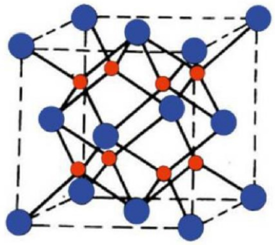
Figure 1.
The structure of an alumina cell.
2.2. Application of Boundary Conditions
CASTEP is a basic program of modern quantum mechanics especially designed for solid materials science. It uses the density functional plane wave pseudopotential method to perform first-principles quantum mechanics calculations. It can explore the crystal and surface properties of materials such as semiconductors, ceramics, metals and minerals. Typical applications include research on surface chemistry, bond structure, density of states and optical properties.
The energy task in CASTEP allows one to calculate the total energy and physical properties of a specific system. In addition to the total energy, the force acting on the atom can be reported after the calculation, and a charge density file can also be created.
The properties task in CASTEP allows the electronic and structural properties to be calculated after the energy operation is completed.
According to Formula (1), the corresponding energy value in the CASTEP module can be obtained by:
where W is the electric field energy per unit volume, ε is the absolute permittivity of a dielectric, D is the electric displacement vector, and E is the electric field intensity.
There are two external conditions for flash sintering: electric field intensity and external temperature. Therefore, we also need to apply these two boundary conditions to the model in the simulation process. When using Material Studio software, we need to build a geometric model of alumina first. Then we need to open the CASTEP simulation module and set the boundary conditions.
The electric field intensity applied in the CASTEP module is 150 eV/Â/e and 450 eV/Â/e. eV/Â/e is the unit of electric field intensity, which is another form of an electric field intensity unit.
According to the relevant temperature conversion formula, the temperature can be converted to thermodynamic temperature. Therefore, the thermodynamic temperature results of 369 °C and 440 °C under the experimental conditions are 642 K and 713 K.
2.3. Simulation Results and Discussion
By changing electric field intensity and temperature, the change graph of the alumina unit cell is shown in Figure 2. The external conditions corresponding to (a–d) are low temperature and low electric field intensity, low temperature and high electric field intensity, high temperature and low electric field intensity and high temperature and high electric field intensity. In Table 3, the lattice in the three-dimensional space generally has three lattice constants, which are represented by a, b and c, respectively, and V represents the volume of the unit cell. The unit of lattice constant is usually  which is a unit of length. The lattice constant refers to the physical size of the unit cell in the crystal lattice. It can be seen from Figure 2 and Table 3 that under high temperature and high electric field intensity, the bond length shrinks and the volume of the unit cell becomes smaller. This makes the arrangement of atoms closer together. It can be concluded that the unit cells are arranged more closely after the material is densified under high temperature and high electric field intensity.
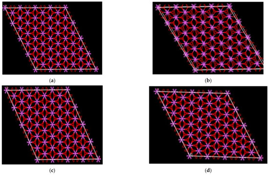
Figure 2.
The change graph of the alumina unit cell. (a) The simulation graph at low temperature and low electric field intensity; (b) the simulation graph at low temperature and high electric field intensity; (c) the simulation graph at high temperature and low electric field intensity; (d) the simulation graph at high temperature and high electric field intensity.
Table 3.
The relationship between unit cell volume and variables.
Figure 3 shows the change in the bond length of the alumina unit cell under changes in temperature and electric field intensity. The blue line in the figure represents probability density, and the red line represents smoothed probability density. We only need to look at the first peak coverage value. It can be seen from Figure 3 that the bond length of the first graph is between 1.7 and 1.74, and the bond length of the second graph is between 1.68 and 1.72. The bond length of the third picture is between 1.67–1.7, and the fourth picture is between 1.6–1.63. It can be seen that under high temperature and high electric field intensity, the bond length is shortened. The size of the unit cell decreases, causing the atoms to be more closely aligned. With the increase of temperature and electric field intensity, the arrangement of atoms in the cell becomes more and more compact. When the variable increases to the peak, the density no longer changes. This is consistent with the analysis of the influence of external factors on atomic volume changes in Section 3 of this paper.
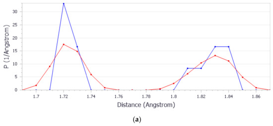
Figure 3.
The change graph of bond length. (a) The simulation graph at low temperature and low voltage; (b) the simulation graph at low temperature and high voltage; (c) the simulation graph at high temperature and low voltage; (d) the simulation graph at high temperature and high voltage.
There are six material transport methods, which are surface diffusion, lattice diffusion (starting from the surface), gas-phase transport, grain boundary diffusion, lattice diffusion (starting from grain boundary) and plastic flow. The mass transfer mechanisms of these six modes are shown in Table 4.
Table 4.
The mass transfer mechanism of flash sintering.
Sintering is an irreversible process. Like other irreversible processes, sintering is mainly due to its own energy reduction. The method that can reduce energy is called the sintering driving force. The three possible driving forces for sintering are particle surface curvature, applied pressure and chemical reaction. Densification means that the ratio of the atomic volume to the unit cell volume increases and the atomic gap decreases. Therefore, the densification of crystals means the reduction of atomic gaps, and macroscopically, the reduction of solid gaps. Through the above-mentioned physical process, the pores are gradually reduced and eliminated. This mass transfer process transports particles from the particles to the pores between the particles. The transfer of matter is driven by the reduction of surface energy, and the energy required for this process is obtained by external heating. The material is transported from a high chemical potential to a low chemical potential. Under normal circumstances, the material will have an obvious sintering phenomenon at about half the melting point. Of course, this process has a lot to do with the grain size of the sintered material. When the particle size is smaller, the surface area becomes larger, and more energy is absorbed. The increase of the energy obtained per unit area will reduce the sintering temperature.
3. Electrical Behavior during Flash Sintering
COMSOL Multiphysics is a powerful multiphysics simulation software that can simulate the physical processes in multiple fields. The flash sintering model involves electrical, thermal and other physical fields, and therefore Joule heat and thermal expansion physical fields were selected in COMSOL. The “Joule Heating and Thermal Expansion” multiphysics interface combines thermal, electrical and structural multiphysics effects. The predefined interaction adds electromagnetic losses in the electric field as a heat source. In addition, the temperature in the “solid heat transfer” interface acts as a thermal load for the “solid mechanics” interface, causing thermal expansion.
3.1. Simulation Setup and Procedure
Generally speaking, the simulation in COMSOL needs four steps: the construction of a geometric model, the addition of materials, the setting of boundary conditions and the division of mesh. Firstly, a simple cuboid was set up as the sample in the simulation process, which is 1 μm in height and 2.5 μm in length and width. The simulation model is shown in Figure 4.
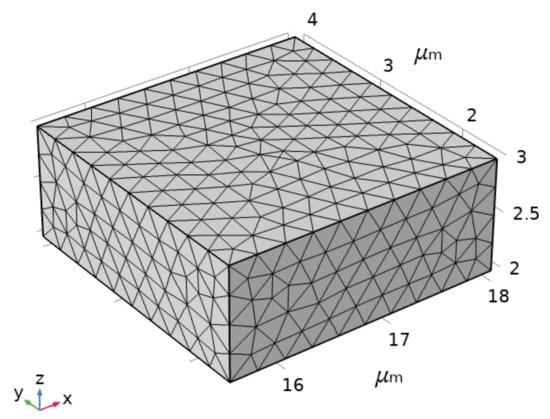
Figure 4.
The meshing of the geometric model.
The second step is the addition of materials. During the flash sintering, the sample is alumina. Therefore, it is necessary to add alumina material to the established geometric model. The specific parameters of the alumina material are shown in Table 5.
Table 5.
The parameters of alumina.
The third step is the setting of boundary conditions. The applied voltage is applied to the two sides of the cuboid along the X-axis. One of the faces is used as input and the other face is used as output. The purpose of changing the electric field intensity can be achieved by changing the magnitude of the voltage during the simulation. The voltage set during the simulation is 0.0375 V and 0.075 V. The conductivity of alumina increases as the temperature rises. Therefore, we need to set the conductivity of alumina to user-defined. This step can be achieved in the conduction current column. In this way, the conduction current during the simulation will increase as the temperature increases.
Under the solid heat transfer node of the Model Builder window, both the initial temperature value and the heat flux were set to 800 K. The purpose is to provide the initial temperature at the time of flash sintering and to keep the entire geometric model at this temperature. For the heat transfer equation, the heat flux boundary condition with a heat transfer coefficient h of 5 W/(m2·K) is used to simulate convective air cooling in other boundaries.
The fourth step is the division of mesh. The accuracy of obtained results based on the finite element analysis model is directly related to the finite element mesh. With the continuous refinement of the grid, these elements become smaller and smaller, and thus the result of the solution approaches reality. The mesh refinement process is a key step to verify the finite element model and ensure the credibility of the model and calculation results. In order to ensure the accuracy of the model and save the simulation time, free tetrahedral mesh is used for simulation, and its size is set as the conventional size. The meshing of the geometric model is shown in Figure 4.
3.2. Simulation Results and Discussion
3.2.1. The Influence of Electric Field Intensity
When the voltage is 0.075 V, indicating that the electric field intensity is equal to 300 V/cm, the change of the current density through the sample changing with time is shown in Figure 5. The current density increases first and then decreases with time, and finally tends to be stable. This curve can be divided into three stages: 0–0.25 s as stage 1, 0.25–0.5 s as stage 2 and 0.5 s and later as stage 3.
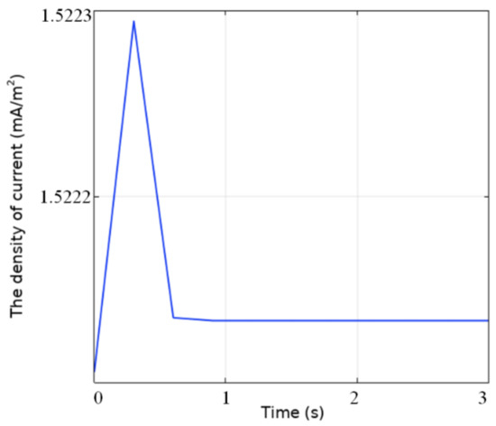
Figure 5.
The change of current density with time when the electric field intensity is 300 V/cm.
Stage 1 is a stage before the occurrence of flash sintering, called the incubation stage of flash sintering. The power supply is under voltage control, and the sample is mainly heated by Joule heat. At this stage, the current density and the power are increasing. Stage 2 is the stage of occurrence of flash sintering. As Joule heat is generated, the temperature in the sample gradually increases until it reaches the threshold for flash sintering. At this stage, rapid shrinking of the sample volume, grain growth and electroluminescence can be observed. In order to avoid the infinite increase of current density, a current density threshold is generally set artificially to protect the experimental equipment. When the current reaches the threshold, it will enter stage 3. Stage 3 is the adiabatic stage, in which the electric field intensity and current density remain stable.
With the electric field intensity of 150 V/cm by changing the voltage, the curve of the current density through the sample changing with time is shown in Figure 6. Compared with Figure 5, it can be observed that the electric field intensity becomes smaller and the time during the incubation phase becomes larger. It shows that the electric field intensity will affect the incubation time of the sample. The greater the electric field intensity, the shorter the incubation time. It is worth noting that in the actual situation, the current density in the stable phase should remain unchanged. However, considering that the current density in the final stage cannot be set in the simulation, the current density in the stable stage is different in the simulation.
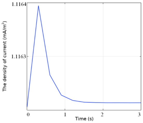
Figure 6.
The change of current density with time when the electric field intensity is 150 V/cm.
Through the simulation, it is found that when the magnitude of the electric field intensity is changed, the displacement of the sample surface remains unchanged, as shown in Figure 7. It shows that the electric field intensity will not affect the grain size of the sample.
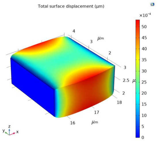
Figure 7.
The displacement of the sample surface when the electric field intensity is 300 V/cm.
Liu Guangxin [35] took 8YSZ ceramics as the research object. The current through the sample was set to 0.05 A, and the electric field intensity was set to 190 V/cm, 255 V/cm and 325 V/cm, respectively. The curve of the current density changing with the flash sintering time was obtained. The curve of current density is consistent with the curve in this paper, and both of them have a sudden change. The results show that the electric field intensity does not change the density, and the electric field intensity determines the incubation time. This is consistent with the simulation results in this paper.
In the flash sintering process, because of the rapid increase of power density in the sample, it is a challenge to accurately measure the temperature of the sample. Therefore, the finite element simulation method was used to measure the temperature of the sample. When the electric field intensity is equal to 300 V/cm, the distribution of the sample surface at the stable stage is shown in Figure 8. Through the finite element simulation analysis of the flash sintering process, the results show that there is a temperature gradient between the surface and the inside of the sample, and the temperature of many parts in the sample surface is greater than 800 K. In [36], the flash sintering process was analyzed by the finite element method. The simulation results show that when the electric field intensity is 120 V/cm, the maximum temperature of the sample reaches 1840 K, which is much higher than 1390 K at the beginning. There are obvious thermal gradients on the surface and inside of the strip specimen. Even on the surface, the temperature gradually decreases from the center to the edge. This is consistent with our results.
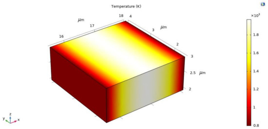
Figure 8.
The temperature distribution of the specimen when the electric field intensity is 300 V/cm.
It can be explained by Joule heating occurring inside the sample. When current flows through the sample, the sample generates a large amount of Joule heat. Joule heat will generate a lot of heat and cause the temperature to rise, which will further reduce the resistivity of the conductor. When the electric field intensity is constant, according to P = U2/R, the thermal effect of electric energy will increase, and the temperature will also increase. It is positive feedback, and thermal runaway of Joule heat will occur, causing the temperature in the sample to increase continuously. Rachman C [37] proposed the densification mechanism of ceramic powder used in the flash sintering process. He analyzed that due to Joule heating, the particles may melt in contact. The conductivity of alumina increases by three orders of magnitude from solid to liquid, which will lead to the thermal runaway effect.
Although the Joule heating effect can explain this phenomenon well, it cannot be considered that the mechanism of flash sintering is the Joule heating effect because of the existence of electroluminescence. There are certainly other mechanisms for flash sintering. Many scholars have also proposed the rapid densification effect, electrochemical reduction, Frenkel pairs and so on [38].
3.2.2. The Influence of Current Density
Similarly, the current density is also a decisive factor for the temperature of the sample. The higher the current density, the higher the temperature of the sample. By keeping the conductivity of the sample constant, the current density of the sample is kept at 1.74 A/m2. The displacement of the sample surface at this time is shown in Figure 9.
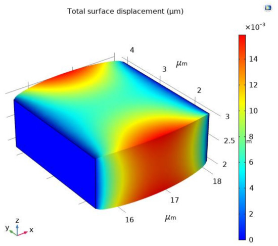
Figure 9.
The displacement of the sample surface when the electric field intensity is 150 V/cm.
By comparing Figure 7 and Figure 9, it can be found that the current density becomes smaller and the displacement of the sample surface also becomes smaller. In other words, the current density will affect the grain size of the sample surface. The greater the current density, the greater the grain size of the sample surface.
In [39], the effect of current density on the densification of samples was obtained under constant applied electric field intensity and furnace temperature of 900 °C. The results show that the density varies with the current density. It is consistent with the simulation results.
After the chemical composition of the ceramic material is determined, the performance of the ceramic material depends on the microstructure of the material. The influence of the preparation process of ceramics on the microstructure of ceramic materials is very important. The preparation process is the main means to control the microstructure of ceramic materials. Sintering is the most critical process for the formation of ceramic microstructures, and it is also the most critical process for imparting various special properties to materials. Therefore, the sintering process of ceramic material has a significant effect on ceramic properties.
Studies have shown that for the ceramic insulator sample of alumina, if the grain size of the sample is smaller, the size distribution is more uniform, and the fewer pores there are in the crystal, the lower the surface charge is [40]. The corresponding along-surface flashover voltage is higher.
Therefore, from the above research, we can conclude that the ceramic insulator prepared by flash sintering technology has higher insulation characteristics. The ceramic insulator used in a power grid can avoid flashover and insulator failure under overvoltage. After long-term operation under the specified mechanical and electrical loads and various environmental conditions, this insulator does not produce obvious deterioration, thus reducing the maintenance cost of the insulator and improving the service life of the insulator.
4. Conclusions
This paper studies the flash sintering technology of ceramic insulators through simulation. Using Material Studio, the unit cell model of alumina was established. The effects of temperature and electric field intensity on the alumina unit cell and bond length were analyzed. COMSOL Multiphysics was used to simulate the flash sintering of ceramic insulators, and the effects of electric field intensity and current density on the flash sintering process were studied. By changing the electric field intensity and current density to measure the temperature change during the flash sintering process, the temperature distribution characteristics during the flash sintering process were obtained. The specific conclusions are as follows:
- (1)
- Under high temperature and high electric field intensity, the bond length is reduced and the volume of the unit cell becomes smaller. The atoms are arranged closer together.
- (2)
- The magnitude of the electric field intensity determines the incubation time of flash sintering. The greater the electric field intensity, the shorter the incubation time. The electric field intensity does not affect the density and grain size of the sample.
- (3)
- The current density determines the density and grain size of the final sample.
- (4)
- There is a temperature gradient between the surface and the inside of the sample.
- (5)
- The ceramic insulator prepared by flash sintering has higher density and smaller grain size. This makes ceramic insulators have better insulation properties. It is not easy for surface discharge to occur.
Author Contributions
Conceptualization, Y.L. and X.H.; methodology, Y.L. and X.H.; software, X.H.; data curation, Y.L. and X.H.; formal analysis, Y.L. and X.H.; investigation, Y.L. and X.H.; writing—Original draft preparation, X.H.; writing—Review and editing, Y.L.; supervision, Y.L.; project administration, Y.L.; funding acquisition, Y.L. All authors have read and agreed to the published version of the manuscript.
Funding
This research was funded by the Chinese National Natural Science Foundation (Grant 51677128) and the Key Research and Development Program of Tianjin (Grant 19YFHBQY00030).
Institutional Review Board Statement
Not applicable.
Informed Consent Statement
Not applicable.
Data Availability Statement
Not applicable.
Conflicts of Interest
The authors declare no conflict of interest.
References
- Jiang, X.; Shi, Y.; Sun, C.; Zhang, Z. Evaluating the Safety Condition of Porcelain Insulators by the Time and Frequency Characteristics of LC Based on Artificial Pollution Tests. IEEE Trans. Dielectr. Electr. Insul. 2010, 17, 481–489. [Google Scholar] [CrossRef]
- Meng, Y.; Gong, G.; Wu, Z.; Yin, Z.; Xie, Y.; Liu, S. Fabrication and Microstructure Investigation of Ultra-high-strength Porcelain Insulator. J. Eur. Ceram. Soc. 2012, 32, 3043–3049. [Google Scholar] [CrossRef]
- Okubo, H. Enhancement of Electrical Insulation Performance in Power Equipment Based on Dielectric Material Properties. IEEE Trans. Dielectr. Electr. Insul. 2012, 19, 733–754. [Google Scholar] [CrossRef]
- Liu, Y.; Du, B.X. Recurrent Plot Analysis of Leakage Current on Flashover Performance of Rime-iced Composite Insulator. IEEE Trans. Dielectr. Electr. Insul. 2010, 17, 465–472. [Google Scholar] [CrossRef]
- Naito, K.; Morita, K.; Hasegawa, Y.; Imakoma, T. Improvement of the DC Voltage Insulation Efficiency of Suspension Insulators under Contaminated Conditions. IEEE Trans. Electr. Insul. 1988, 23, 1025–1032. [Google Scholar] [CrossRef]
- Zedan, F.; Akbar, M. Performance of HV Transmission Line Insulators in Desert Conditions IV: Study of Insulators at a Semi-coastal Site in the Eastern Region of Saudi Arabia. IEEE Trans. Power Deliv. 1991, 6, 70–71. [Google Scholar] [CrossRef]
- Trunec, M.; Maca, K. Compaction and Pressureless Sintering of Zirconia Nanoparticles. J. Am. Ceram. Soc. 2010, 90, 2735–2740. [Google Scholar] [CrossRef]
- Zhou, M.; Huang, Z.; Qi, J.; Wei, N.; Wu, D.; Zhang, Q.; Wang, S.; Feng, Z.; Lu, T. Densification and Grain Growth of Gd2Zr2O7, Nanoceramics during Pressureless Sintering. J. Eur. Ceram. Soc. 2017, 37, 1059–1065. [Google Scholar] [CrossRef]
- Li, J.; Ye, Y. Densification and Grain Growth of Al2O3 Nanoceramics during Pressureless Sintering. J. Am. Ceram. Soc. 2006, 89, 139–143. [Google Scholar] [CrossRef]
- Maca, K.; Trunec, M.; Dobsak. Bulk Zirconia Nanoceramics Prepared by Cold Isostatic Pressing and Pressureless Sintering. Rev. Adv. Mater. Sci. 2005, 10, 84–89. [Google Scholar]
- Skandan, G.; Hahn, H.; Kear, B.H.; Roddy, M.; Cannon, W.R. Processing of Nanostructured Zirconia Ceramics. Nanostruct. Mater. 1994, 351, 111–126. [Google Scholar] [CrossRef]
- Hynes, A.P.; Doremus, R.H.; Siegel, R.W. Sintering and Characterization of Nanophase Zinc Oxide. J. Am. Ceram. Soc. 2010, 85, 1979–1987. [Google Scholar] [CrossRef]
- Betz, U.; Sturm, A.; Loeffler, J.; Wagner, W.; Wiedenmann, A.; Hahn, H. Low-temperature Isothermal Sintering and Microstructural Characterization of Nanocrystalline Zirconia Ceramics Using Small Angle Neutron Scattering. Nanostruct. Mater. 1999, 12, 689–692. [Google Scholar] [CrossRef]
- Kuang, X.; Carotenuto, G.; Nicolais, L. A Review of Ceramic Sintering and Suggestions on Reducing Sintering Temperatures. Adv. Perform. Mater. 1997, 4, 257–274. [Google Scholar] [CrossRef]
- Bourell, D.L.; Parimal; Kaysser, W. Sol–gel Synthesis of Nanophase Yttria-stabilized Tetragonal Zirconia and Densification Behavior Below 1600 K. J. Am. Ceram. Soc. 1993, 76, 705–711. [Google Scholar] [CrossRef]
- Kear, B.; Colaizzi, J.; Mayo, W.; Liao, S.-C. On the Processing of Nanocrystalline and Nanocomposite Ceramics. Scripta Mater. 2001, 44, 2065–2068. [Google Scholar] [CrossRef]
- Ehre, D.; Gutmanas, E.Y.; Chaim, R. Densification of Nanocrystalline MgO Ceramics by Hot-pressing. J. Eur. Ceram. Soc. 2005, 25, 3579–3585. [Google Scholar] [CrossRef]
- Sarrafi, M.H.; Bafrooei, H.B.; Feizpour, M.; Ebadzadeh, T.; Foroush, M.H. Microwave Synthesis and Sintering of Mg4Nb2O9, Nanoceramics. J. Mater. Sci. Mater. Electron. 2014, 25, 946–951. [Google Scholar] [CrossRef]
- Bykov, Y.; Eremeev, A.; Egorov, S.; Ivanov, V.; Kotov, Y.; Khrustov, V.; Sorokin, A. Sintering of Nanostructural Titanium Oxide Using Millimeter-wave Radiation. Nanostruct. Mater. 1999, 12, 115–118. [Google Scholar] [CrossRef]
- Paranosenkov, V.P.; Kelina, I.Y.; Plyasunkova, L.A.; Bykov, Y.V. Preparation of Dense Ceramics Based on Silicon Nitride Nanopowders. Refract. Ind. Ceram. 2003, 44, 223–226. [Google Scholar] [CrossRef]
- Mishra, R.; Schneider, J.; Shackelford, J.; Mukherjee, A. Plasma Activated Sintering of Nanocrystalline γ-Al2O3. Nanostruct. Mater. 1995, 5, 525–544. [Google Scholar] [CrossRef]
- Suganuma, M.; Kitagawa, Y.; Wada, S.; Murayama, N. Pulsed Electric Current Sintering of Silicon Nitride. J. Am. Ceram. Soc. 2010, 86, 387–394. [Google Scholar] [CrossRef]
- Kimura, H.; Hongo, K. In Process Nanocrystalline Control Consolidation of the Amorphous ZrO2–20 mol% Al2O3 Powder. Mater. Trans. 2006, 47, 1374–1379. [Google Scholar] [CrossRef]
- Cernea, M.; Fochi, F.; Aldica, G.V.; Vasile, B.S.; Trusca, R.; Galassi, C. Spark–Plasma-Sintering Temperature Dependence of Structural and Piezoelectric Properties of BNT–BT0. 08 Nanostructured Ceramics. J. Mater. Sci. 2012, 47, 3669–3673. [Google Scholar] [CrossRef]
- Munir, Z.A.; Anselmi–Tamburini, U.; Ohyanagi, M. The Effect of Electric Field and Pressure on the Synthesis and Consolidation of Naterials: A Review of the Spark Plasma Sintering Method. J. Mater. Sci. 2006, 41, 763–777. [Google Scholar] [CrossRef]
- Cologna, M.; Francis, J.S.C.; Raj, R. Field Assisted and Flash Sintering of Alumina and Its Relationship to Conductivity and MgO-doping. J. Eur. Ceram. Soc. 2011, 31, 2827–2837. [Google Scholar] [CrossRef]
- M’Peko, J.C.; Francis, J.S.C.; Raj, R. Field–assisted Sintering of Undoped BaTiO3: Microstructure Evolution and Dielectric Permittivity. J. Eur. Ceram. Soc. 2014, 34, 3655–3660. [Google Scholar] [CrossRef]
- Zapata-Solvas, E.; Bonilla, S.; Wilshaw, P.; Todd, R. Preliminary Investigation of Flash Sintering of SiC. J. Eur. Ceram. Soc. 2013, 33, 2811–2816. [Google Scholar] [CrossRef]
- Prette, A.L.; Cologna, M.; Sglavo, V.M.; Raj, R. Flash-sintering of Co2MnO4, Spinel for Solid Oxide Fuel Cell Applications. J Power Source 2011, 196, 2061–2065. [Google Scholar] [CrossRef]
- Grasso, S.; Saunders, T.; Porwal, H.; Cedillos-Barraza, O.; Jayaseelan, D.D.; Lee, W.E.; Reece, M.J. Flash Spark Plasma Sintering (FSPS) of Pure ZrB2. J. Am. Ceram. Soc. 2014, 97, 2405–2408. [Google Scholar] [CrossRef]
- Ojaimi, C.L.; Ferreira, J.A.; Chinelatto, A.L.; Chinelatto, A.S.A.; Pallone, E.M.D.J.A. Microstructural Analysis of ZrO2/Al2O3 Composite: Flash and Conventional Sintering. Ceram. Int. 2020, 46, 2473–2480. [Google Scholar] [CrossRef]
- Egorov, S.; Eremeev, A.; Kholoptsev, V.; Plotnikov, I.; Rybakov, K.; Sorokin, A.; Bykov, Y. On the Correlation Between the Thermal Instability Onset and the Flash Sintering Event. Scr. Mater. 2020, 174, 68–71. [Google Scholar] [CrossRef]
- Cologna, M.; Rashkova, B.; Raj, R. Flash Sintering of Nanograin Zirconia in <5 s at 850 Degrees. Am. Ceram. Soc. 2010, 93, 3556–3559. [Google Scholar]
- Zapata-Solvas, E.; Gómez-García, D.; Domínguez-Rodríguez, A.; Todd, R.I. Ultra-fast and energy-efficient sintering of ceramics by electric current concentration. Sci. Rep. 2015, 5, 8513. [Google Scholar] [CrossRef] [PubMed]
- Liu, G. Research on Temperature Field of 8YSZ Ceramics during Flash Sintering. Master’s Thesis, Southwest Jiaotong University, Chengdu, China, 2018. [Google Scholar]
- Li, J.; Guan, L.; Zhang, W.; Luo, M.; Song, J.; Song, X.; An, S. Sintering behavior of samarium doped ceria under DC electrical field. Ceram. Int. 2018, 44, 2470–2477. [Google Scholar] [CrossRef]
- Rachman, C. Liquid Film Capillary Mechanism for Densification of Ceramic Powders during Flash Sintering. Materials 2016, 9, 280. [Google Scholar]
- Yu, M.; Grasso, S.; McKinnon, R.; Saunders, T.; Reece, M.J. Review of Flash Sintering: Materials, Mechanisms and Modelling. Adv. Appl. Ceram. 2017, 116, 24–60. [Google Scholar] [CrossRef]
- Francis, J.S.C.; Raj, R. Influence of the Field and the Current Limit on Flash Sintering at Isothermal Furnace Temperatures. J. Am. Ceram. Soc. 2013, 96, 2754–2758. [Google Scholar] [CrossRef]
- Ding, L.; Li, C.; Wang, J.; Wang, W. Influence of Sintering Temperature on the Flashover Performance of Alumina Insulators in Vacuum. IEEE Trans. Dielectr. Electr. Insul. 2002, 9, 182–186. [Google Scholar] [CrossRef]


Publisher’s Note: MDPI stays neutral with regard to jurisdictional claims in published maps and institutional affiliations. |
© 2021 by the authors. Licensee MDPI, Basel, Switzerland. This article is an open access article distributed under the terms and conditions of the Creative Commons Attribution (CC BY) license (http://creativecommons.org/licenses/by/4.0/).