Figure 1.
Tapped-inductor buck current converter topology and its operation states. (a) Tapped-inductor buck current converter topology; (b) S2 in on-state and S1 in off-state; (c) S2 in off-state and S1 in on-state.
Figure 1.
Tapped-inductor buck current converter topology and its operation states. (a) Tapped-inductor buck current converter topology; (b) S2 in on-state and S1 in off-state; (c) S2 in off-state and S1 in on-state.
Figure 2.
Tapped-inductor boost current converter topology and its operation states. (a) Tapped-inductor boost current converter topology; (b) in on-state and in off-state; (c) in off-state and in on-state.
Figure 2.
Tapped-inductor boost current converter topology and its operation states. (a) Tapped-inductor boost current converter topology; (b) in on-state and in off-state; (c) in off-state and in on-state.
Figure 3.
Tapped-inductor buck-boost current converter topology and its operation states. (a) Tapped-inductor buck-boost current converter topology; (b) in on-state and in off-state; (c) in off-state and in on-state.
Figure 3.
Tapped-inductor buck-boost current converter topology and its operation states. (a) Tapped-inductor buck-boost current converter topology; (b) in on-state and in off-state; (c) in off-state and in on-state.
Figure 4.
Conventional Boost current converter topology and its operation states. (a) Conventional Boost current converter topology; (b) S1 in on-state; (c) S1 in off-state.
Figure 4.
Conventional Boost current converter topology and its operation states. (a) Conventional Boost current converter topology; (b) S1 in on-state; (c) S1 in off-state.
Figure 5.
Characteristic of the Conventional Boost current converter, the Current gain with duty ratio of conventional boost current converter.
Figure 5.
Characteristic of the Conventional Boost current converter, the Current gain with duty ratio of conventional boost current converter.
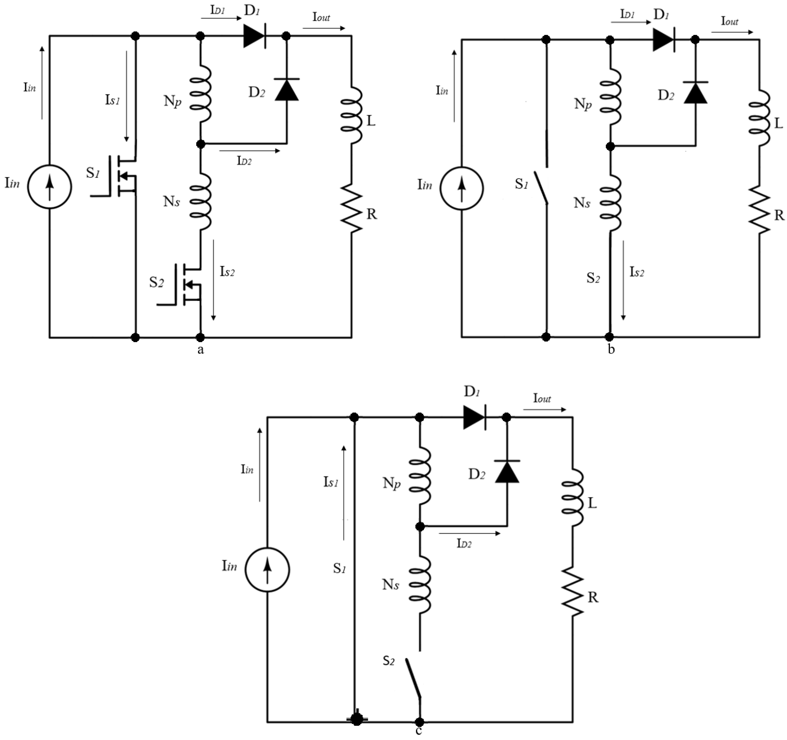
Figure 6.
Tapped-inductor Boost current converter topology and its operation states. (a) Tapped-inductor Boost current converter topology; (b) S1 is in off-state and S2 is in on-state; (c) S1 is in on-state and S2 is in off-state.
Figure 6.
Tapped-inductor Boost current converter topology and its operation states. (a) Tapped-inductor Boost current converter topology; (b) S1 is in off-state and S2 is in on-state; (c) S1 is in on-state and S2 is in off-state.
Figure 7.
Current gain with turns ratio of Tapped-inductor boost current converter.
Figure 7.
Current gain with turns ratio of Tapped-inductor boost current converter.
Figure 8.
Tapped-inductor boost current converter topology with parasitic components.
Figure 8.
Tapped-inductor boost current converter topology with parasitic components.
Figure 9.
Tapped-inductor Boost current converter topology.
Figure 9.
Tapped-inductor Boost current converter topology.
Figure 10.
Measured waveforms of the experimental of the tapped-inductor boost current converter. (a) Top trace: Iout (5 μs/500 mA/div); middle trace: VGS of S1 switch (5 μs/20 V/div); bottom trace: VDS of S1 (5 μs/100 V/div); (b) Top trace: Iout (5 μs/500 mA/div); middle trace: VGS of S2 switch (5 μs/20 V/div); bottom trace: VDS of S2 (5 μs/20 V/div); (c) Top trace: VGS of S1 switch (5 μs/10 V/div); bottom trace: VDS of S2 (5 μs/10 V/div).
Figure 11.
Conventional boost current converter topology.
Figure 11.
Conventional boost current converter topology.
Figure 12.
Analysis the current gain of the Tapped-inductor boost current converter with duty ratio. (a) Comparison of the current gain in between the simulated results and the experimental results ( = 1 A and R = 5 ); (b) Simulated results of the current gain with different input currents.
Figure 12.
Analysis the current gain of the Tapped-inductor boost current converter with duty ratio. (a) Comparison of the current gain in between the simulated results and the experimental results ( = 1 A and R = 5 ); (b) Simulated results of the current gain with different input currents.
Figure 13.
Comparison of power conversion efficiency. (a) Compared with the experimental results of the Conventional and Tapped-inductor boost current converters under Iin = 1 A, R = 5 ; (b) Compared with the simulated results of the Conventional and Tapped-inductor boost current converters under Iin = 1 A, R = 5 ; (c) Compared with the simulated results with different input currents Iin with R = 5 .
Figure 14.
(a) Compared with the experimental results of the Output current ripples of the Conventional and Tapped-inductor boost current converters under Iin = 1 A and R = 5 ; (b) Compared with the simulated results of the Output current ripples of the Conventional and Tapped-inductor boost current converters under = 1 A and R = 5 .
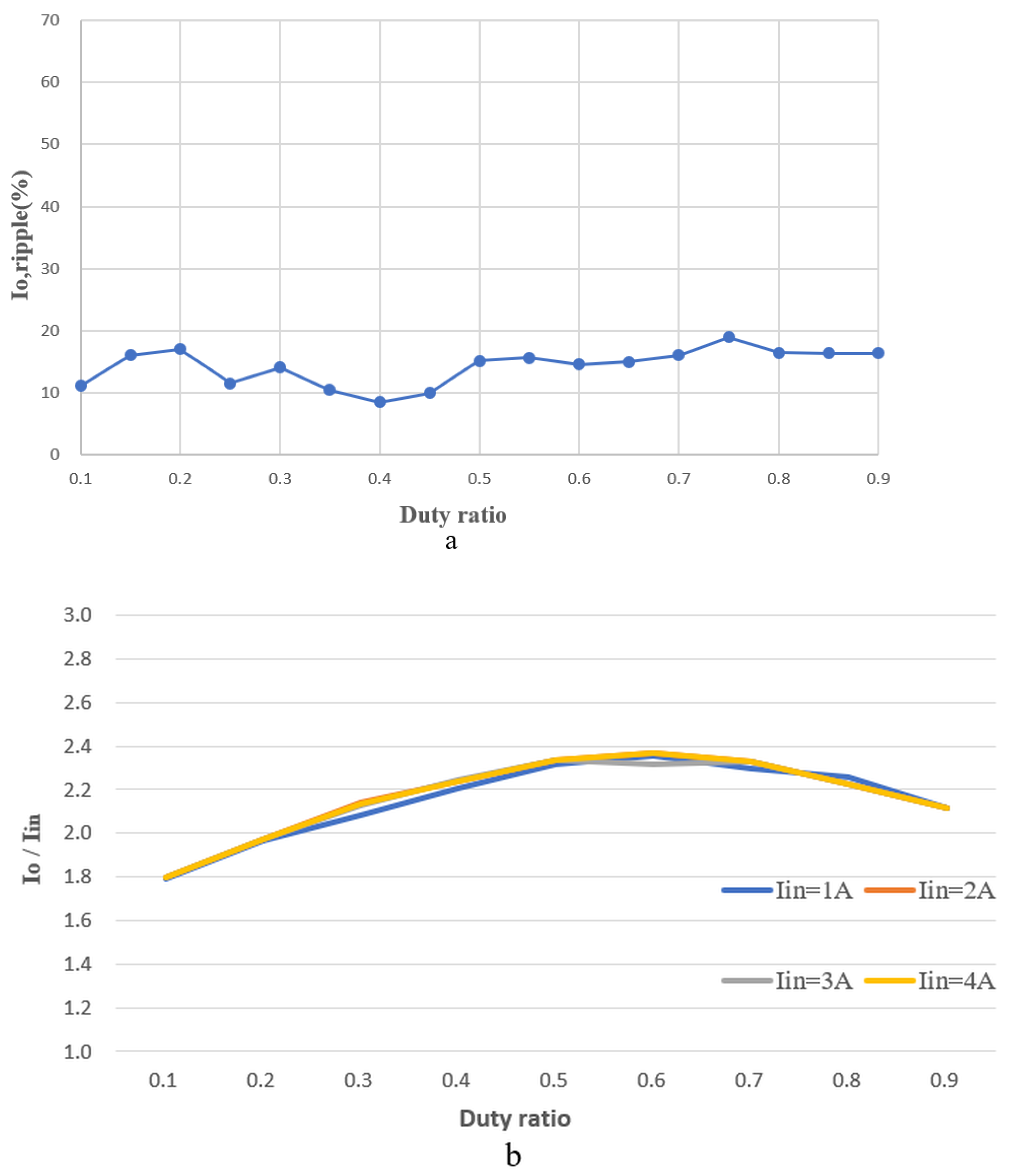
Figure 15.
Experimental and simulated results of Tapped-inductor boost current converter with loading effect analysis. (a) Output current ripple of the converter under Iin = 1 A and R = 10 ; (b) Current conversion ratio of the converter with different Iin.
Figure 15.
Experimental and simulated results of Tapped-inductor boost current converter with loading effect analysis. (a) Output current ripple of the converter under Iin = 1 A and R = 10 ; (b) Current conversion ratio of the converter with different Iin.
Table 1.
Parameters used in simulation—Conventional boost current converter.
Table 1.
Parameters used in simulation—Conventional boost current converter.
| Duty Ratio | 0.1–0.9 |
| Load R () | 5 |
| Capacitance C (F) | 30 |
| Inductance L (mH) | 1.53 |
Table 2.
Parameters used in simulations—Tapped-inductor boost current converter.
Table 2.
Parameters used in simulations—Tapped-inductor boost current converter.
| Load R () | 5 |
| Switching frequency (kHz) | 100 |
| Turns Ratio of the tapped-inductor | 0.7 |
| Output Inductive filter L (mH) | 1.53 |
Table 3.
Parasitic components used in simulations—Tapped-inductor boost current converter.
Table 3.
Parasitic components used in simulations—Tapped-inductor boost current converter.
| (m) | 58 |
| (m) | 58 |
| () | 0.4 |
| () | 0.2 |
| () | 0.1 |
| (V) | 0.5 |
| (V) | 0.5 |
Table 4.
Parameters used in experiments.
Table 4.
Parameters used in experiments.
| Duty Ratio | 0.1–0.9 |
| Load R () | 5 |
| Switching frequency (kHz) | 100 |
| Turns Ratio of the tapped-inductor | 0.7 |
| Primary inductance, Np (mH) | 62 |
| Secondary inductance, Ns (mH) | 3 |
| Output inductive filter (mH) | 1.53 |
| Switches S1, Rds1 (m) | 58 |
| Switches S2, Rds2 (m) | 58 |
Table 5.
Parameters used in experiments.
Table 5.
Parameters used in experiments.
| Duty Ratio | 0.1–0.9 |
| Load R () | 5 |
| Switching frequency (kHz) | 100 |
| Capacitor C (F) | 30 |
| Output inductive filter L (mH) | 1.53 |
Table 6.
Parameters used in experiments.
Table 6.
Parameters used in experiments.
| Duty Ratio | 0.1–0.9 |
| Load R () | 10 |
| Switching frequency (kHz) | 100 |
| Turns Ratio of the tapped-inductor | 0.7 |
| Primary inductance, Np (mH) | 62 |
| Secondary inductance, Ns (mH) | 3 |
| Output inductive filter L (mH) | 1.53 |
| Switches S1,Rds1 (m) | 58 |
| Switches S2,Rds2 (m) | 58 |


