Abstract
Stray capacitances (SCs) are a serious issue in high-voltage (HV) applications. Their presence can alter the circuit or the operation of a device, resulting in wrong or even disastrous consequences. To this purpose, in this work, we describe the modeling of SCs in HV capacitive dividers. Such modeling does not rely on finite element analysis or complicated geometries; instead, it starts from an equivalent circuit of a conventional measurement setup described by the standard IEC 61869-11. Once the equivalent model including the SCs is found, closed expressions of the SCs are derived starting from the ratio error definition. Afterwards, they are validated in a simulation environment by implementing various circuit configurations. The results demonstrate the expressions applicability and effectiveness; hence, thanks to their simplicity, they can be implemented by system operators, researchers, and manufacturers avoiding the use of complicated methods and technologies.
1. Introduction
The power network has undergone a significant revolution in the last few decades, due to the spread of distributed energy resources (DER) (e.g., almost 35% of the total amount of production in Italy [1]) by intelligent electronic devices (IED), such as energy meters, phasor measurement units (PMUs), etc., and most recently, the introduction of electric vehicles (EVs), with their sales increasing daily. These changes have forced utilities and distribution system operators (DSOs) to rethink ways to manage and control the grid, for all the considered voltage levels, i.e., low, medium, and high (LV, MV, and HV, respectively), to avoid serious complications due to the presence of such new actors within the grid.
In this scenario, instrument transformers (ITs) play a significant role [2,3,4]. In fact, despite the aforementioned changes and modifications of the grid, they must continue, in a reliable way, to operate, scaling voltages (voltage transformers, VTs) and currents (current transformers, CTs) in order to be suitable for the typical acquisition systems, and then to be evaluated by the operators.
ITs rely upon a solid backbone of standards, the IEC 61869 series, comprised of fifteen documents which cover all kind of transformers and their different features and capabilities. For example, Standards IEC 61869-1 and -6 deal with general requirements [5,6] that apply to conventional ITs and low-power ITs (LPITs), respectively; Standards IEC 61869-2 to -5 describe inductive instrument transformers; regarding the new generation of electronic devices, they are standardized in Standards IEC 61869-7 to -15 (including direct current (DC) devices and merging units) [7,8].
In addition to the standards for ITs, there is also extensive related literature with available documents that try to address most of the issues that may affect their correct operation. For example, in [9,10,11,12,13], the effects of temperature on ITs are described; in [14,15,16,17,18,19,20], several modeling methods and procedures are presented, for both CTs and VTs (in both time and frequency domain); finally, [21,22,23,24,25,26] discuss specifically the ITs uncertainty under rated or off-nominal conditions of the grid.
From the literature, emerges the fact that electrical and environmental quantities can affect ITs and their accuracy (of course, within the grid, not only are ITs affected by those quantities, but also other assets, such as electric motors [27,28,29] and accessories [30,31,32,33,34]).
Therefore, accuracy must be treated as a fundamental aspect to deal with whenever applications of ITs are considered; and therefore, in this paper, we focus on an evaluation of how the accuracy of ITs is influenced by some stray parameters. Specifically, in this paper, HV capacitive dividers (CDs) are considered; in particular, stray capacitances between points at different voltages are analyzed and modeled.
It is well-known that measuring high voltage is always a critical task as compared with MV and LV, due to the issues associated the high voltage. Among all the potential ways of measuring HV, CDs are frequently adopted to reduce HV, and therefore are one of the most studied [35,36,37,38,39] (see further details below).
As previously mentioned, stray capacitances are a critical issue related to working with HV and CDs. In fact, they originate and increase as the voltage difference between two points of the circuit increases, introducing new paths for the current, and then modifying the expected operation of the equipment.
Stray capacitances (SCs) have been previously studied in several works. For example, formulae for the capacitances based on the geometries studied are described in [40]. In [41,42,43,44], stray capacitances were modeled for resistive, capacitive–resistive, and capacitive dividers, respectively. In those works, considering the complexity of the capacitance computation, even for simple geometries, the authors treated the stray capacitance identification with finite element methods, or assumed simple geometries as known. However, those approaches are not always possible or available.
In contrast, we aim at simplifying this assessment process, differentiating its content from what can be found in the literature, by avoiding the use of complicated techniques and the need for preliminary knowledge of the equipment and location geometries to deal with. In fact, for this work, we start from a conventional in-field configuration of capacitive dividers, the three-phase configuration of devices, to identify an equivalent circuit of the capacitive dividers which includes the stray capacitances. Afterwards, SCs are estimated starting from accuracy measurements performed on actual CDs and by manipulating the test conditions to extrapolate more information.
The result of our research is a set of closed expressions to find the stray capacitances of the considered circuit, starting from the knowledge of the rated capacitance (visible on the nameplate of the device) of the divider and from the ratio error information (obtained from real in-field or in-laboratory measurements). Then, the obtained expressions could be adopted by manufacturers or researchers to improve the design of CDs for better fulfilling the accuracy test requirements fixed by the standards. In particular, users of CDs may build their own equivalent circuit which includes the SCs that are influencing a CD’s behavior.
The paper is structured as follows: In Section 2, we provide an overview of the basic principles of a capacitive divider; in Section 3, we describe the modeling of the stray capacitances, in which the considered circuit is presented along with all the steps that lead to the final expressions; in Section 4, we validate and discuss the obtained results by means of a simulation environment; and in Section 5, we provide conclusions and some comments are summarized.
2. Capacitive Dividers
2.1. Basic Principles
A CD is a device that uses capacitors (instead of resistors, for example) to reduce a high voltage according to the selected number and values of the capacitors. In detail, the greater amount of voltage drops on the smallest capacitor of the divider (opposite working principle than resistors).
The ideal equivalent circuit is depicted in Figure 1a, where the primary and secondary capacitors can be distinguished ( and , respectively). Furthermore, the diagram also shows the primary high-voltage terminal “A” (hence the HV to be reduced), the secondary low voltage terminal “a” (the reduced voltage), and “n” the common ground or reference terminal.
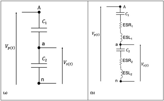
Figure 1.
(a) The ideal equivalent circuit of a capacitive divider; (b) The real equivalent circuit of a capacitive divider.
From Figure 1a it is also possible to write the input/output relation of the ideal divider as follows:
where is the time-dependent output voltage and is the time-dependent primary voltage, to be reduced by the divider. The interesting fact from Equation (1) is that even if the capacitor is a frequency dependent component the frequency does not appear. This is due to the fact that the capacitive divider components are all equally affected by frequency, hence, the frequency dependence of the output voltage disappears.
From Equation (1), it is possible to compute the transformation ratio of the divider (hence the ideal, or expected) as follows:
Therefore, from Equation (2), it is clear that the higher the secondary capacitor the higher the of the overall divider.
Turning to the real CD, note that its equivalent circuit is shown in Figure 1b. Of course, one can complicate the real circuit as much as desired, but the depicted one has been selected due to its typical usage when the real description of the CD is considered. What differs from the ideal circuit is the presence of the equivalent series resistor ESR and the equivalent series inductor ESL for both primary and secondary sides ( and for the primary and and for the secondary, respectively).
The presence of the ESR describes the non-ideality of the capacitor that also consists of conductors or metallic parts that dissipate heat. The presence of the ESL, instead, describes the non-ideality of the capacitor that leads to an autoresonance between the capacitance value of the capacitor and ESL. This resonance value must be selected far from the operating frequency of the considered application.
In light of the non-idealities, Equation (1) becomes the following:
where and are the complex impedances of the primary and secondary side of the circuit, respectively, which include the contributions of the ESR and ESL.
2.2. Pros and Cons
The CD technology is commonly implemented from the LV to the HV due to its advantages with respect to other technologies. Compared to the resistive divider, for example, the CD does not dissipate as much heat, hence, the current circulating through a CD is not a limiting factor. Of course, if the real circuit of the CD is considered, an equivalent resistor is to be considered; however, its contribution to the heat dissipation is negligible as compared with a resistive divider.
Furthermore, CDs can be classified in terms of their loss tangent (or ), which is the ratio between the resistive and the reactive part of a capacitor, which quantifies the “goodness” or the efficiency of the capacitor itself.
Another advantage of a CD is its linearity vs. frequency. In fact, as introduced above, even if the reactance is dependent on the frequency , the ratio of the divider, hence the output of a CD, is not frequency dependent.
On the contrary, among the disadvantages, CDs cannot be implemented into DC applications due to the capacitor nature of blocking DC components. Finally, it should be emphasized that CDs match the above description and advantages as much as they show an ideal behavior; hence, not influenced from the parasitic parameters.
3. Modeling Stray Capacitances
After the brief description of the CDs presented in Section 2, this section contains the core of the work. In detail, after introducing stray capacitances in Section 3.1, in Section 3.2, we describe the considered equivalent circuit. Then, in Section 3.3, we perform a simple circuital analysis to obtain useful information that is used, as described in Section 3.4, to derive the SCs expressions.
3.1. Stray Capacitances
A stray capacitance is an issue that manifests between two points subjected to different potentials, due to the fact that the electric field lines, starting from one point, close themselves to the surrounding points with different potentials. As a matter of fact, this issue is more significant in HV applications such as HV AC measurements (but, of course, SCs affect a wide variety of fields, from telecommunications to microelectronics, etc., even if they are not HV applications).
However, the identification of SCs is a very difficult task for several reasons including the following: (i) SCs are very small capacitances which, due to noise signals and other disturbances, are very difficult to measure and even detect; (ii) even if the approach is numerical, the geometries of the application is not always known, hence, the estimation of a SC is often not 100% correct.
The results of such difficulties impact on the knowledge of the equivalent circuit. In the specific case of a HV divider, it influences the value of the transformation ratio, hence, all the accuracy indexes computed starting from the ratio of the device. In fact, the actual transformation ratio is affected by temperature, humidity, non-idealities, etc., and also the SCs, which modify the equivalent circuit to be considered. In other HV applications, including motors and transformers [45], SCs play a fundamental role in the frequency behavior estimation of such machines.
Therefore, it is important to find simple and sufficiently accurate ways of estimating SCs to fully understand the behavior of electric assets when operating at rated or faulty conditions and, in the case of HV capacitive dividers, how well they measure, hence what is their associated uncertainty.
In [46], for example, the authors evaluated the uncertainty with methods A and B (from the guide of the expression of uncertainty [47]) of a CD but without including stray capacitances.
3.2. Considered Model
In this work, the SC modeling is based on a measurement setup defined in the IEC standard [8] to evaluate the immunity of CDs. Such a setup is schematized in Figure 2 and it consists of the following: (i) a grounded wall indicated with “W”; (ii) the HV divider under test indicated with “DUT” and another identical HV divider used as a dummy divider for the tests, indicated as “DD”.
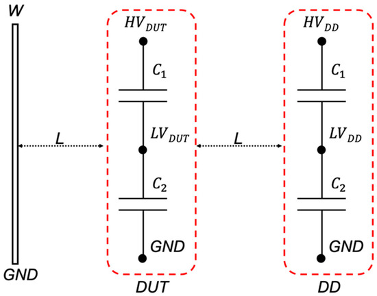
Figure 2.
The measurement setup defined in Standard IEC 61869-11 [8].
In Figure 2, the following can be observed: (i) the fixed distance “L” between the wall and the dividers; (ii) the points where the HV is applied and for the device under test and the dummy one, respectively; and (iii) the LV secondary outputs and . It is important to emphasize that the distance L has been defined by the standard as the distance between two devices operating at the highest rms value of phase-to-phase voltage for which the equipment is designed in respect of its insulation [8].
At this point, the equivalent circuit of Figure 2 has been complicated and completed with the SCs that raise from that circuit. The final schematic is presented in Figure 3.
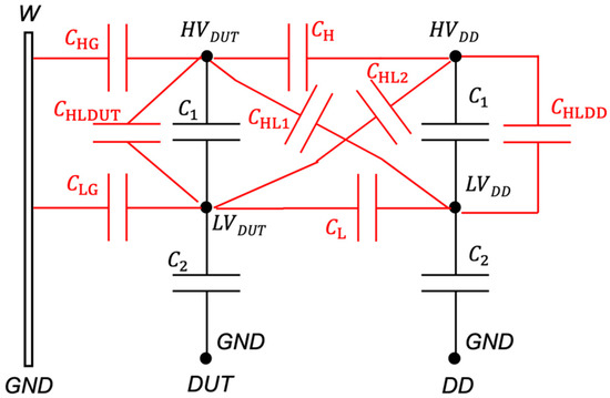
Figure 3.
The equivalent circuit of the setup in Figure 2 including the stray capacitances (SCs).
The SCs, as shown in Figure 3, are listed and described in Table 1 for the sake of clarity. Regarding and , the “*” is to highlight that when the HV is shared between the dividers, as in one of tests described by [8], they do not exist. However, for a complete scenario that includes tests in which the two HVs may be different or with different phases, they have been included in the equivalent circuit.

Table 1.
List of SCs and their meaning.
At a glance, without preliminary studies but from their position, it is possible to predict the SCs that may affect the operation of the dividers, i.e., and . The following sections confirm or confute the hypothesis. It should be noted that, considering the model of Figure 3, more configurations that include SCs can be obtained from the circuit. Therefore, the model is not limited to the presented configuration.
Next, three test conditions are studied and used to obtain the SC expressions. They are listed in Table 2 and they represent a potential operating condition of the setup depicted in Figure 2. In detail, Section 3.3 exploits tests T1 to T3 to derive the CD input/output relation of each circuit. Finally, the results of Section 3.3 are used in Section 3.4 to obtain the SCs expressions.
Table 2.
Description of the test conditions considered in Section 3.2.
3.3. Circuital Analysis with T1, T2, and T3
The main idea of the analysis is to obtain an equivalent circuit which obeys the conditions of the tests in Table 2. Afterwards, for each equivalent circuit, the associated input/output ratio is calculated as follows:
where and are the rms values of the primary and secondary voltage, respectively (see Figure 1).
For the sake of clarity, the defined to describe Figure 1 corresponds to the voltage between and ground; hence, the secondary voltage of the divider under test.
Starting from test T1, the equivalent circuit is depicted in Figure 4. Note, from the circuit, it can be appreciated which capacitors concur to the computation of the secondary voltage.
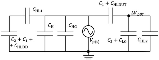
Figure 4.
Equivalent circuit of the test condition T1.
Such capacitors are , , , , and . Therefore, the secondary voltage of the circuit can be written as:
After some manipulation, and moving to a rms representation of the quantities, the ratio defined in Equation (4) can be obtained as:
The calculations to Equation (6) are replicated for T2. The main difference is the presence of two voltage sources which requires the use of the well-known superposition principle. Therefore, the two circuits to be analyzed are shown in Figure 5. Figure 5a represents the condition when the source in is considered, while Figure 5b represents the condition when the source in is used.
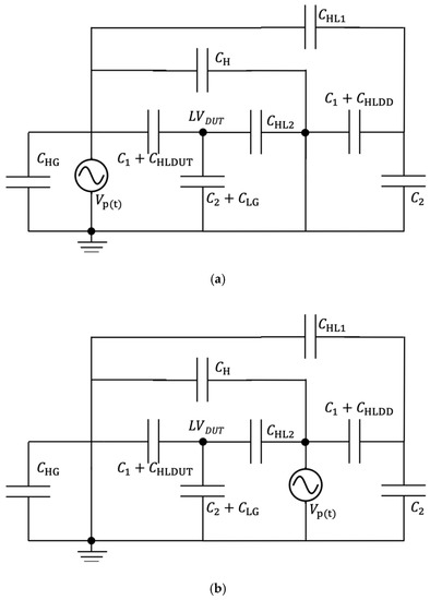
Figure 5.
Equivalent circuit of the test condition T2. (a) When the source is considered; (b) When source is considered.
Once the superposition principle has been applied to the circuits of Figure 5, the overall secondary voltage becomes:
And the ratio is easily found to be:
The last analysis considers the configuration T3 which does not involve the presence of the grounded wall W. Therefore, as previously done, the equivalent circuit without wall is the one presented in Figure 6, where all the symbols have been previously defined.
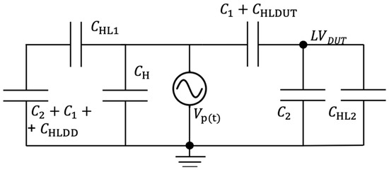
Figure 6.
Equivalent circuit of the test condition T3.
From the circuit, the secondary voltage can be written as follows:
and the ratio can be obtained as:
It is important to highlight that, if in the above expressions of all the SCs are neglected, the rated transformation ratio is easily obtained as in Equation (2).
Equations (2), (6), (8), and (10) are used in Section 3.4 to find the SCs expressions.
3.4. SCs Expressions
In Section 3.3, the actual ratio of the CD has been written in terms of the SCs to highlight their contribution to the ratio. In fact, the actual ratio directly affects the ratio error of the CDs. Therefore, the SC expressions are found by considering the ratio error of the measurements performed on configurations T1 to T3. In other words, let us assume , , and to be the ratio error (as defined in the standard [6]) of measurements on configurations T1, T2, and T3, respectively. Then, the defined ratio errors can be written in terms of the , previously found, as follows:
By substituting the expressions of the inside Equations (11)–(13), one obtains:
Inside the three expressions, the unknowns are exclusively the three SCs. Therefore, solving the linear system of three equations with three unknowns leads to the following:
Despite the complicated appearance, the closed Expressions (17)–(19) can be used to find the SCs of the considered HV circuit, by knowing the ratio error measured for the three configurations T1 to T3 and the primary and secondary capacitance of the adopted divider. It is worthwhile to note that the expressions have been found without knowing the detailed geometry of the equipment and the location. Furthermore, no complicated finite element analysis has been performed.
Another interesting observation is that, if , hence an ideal condition of no SCs in the circuit, Expressions (17)–(19) provides as expected. Therefore, at this point, the theoretical correctness of the closed expression is confirmed.
4. Implementation and Validation
In this section, first of all, measurement results of laboratory experimental activities are used to quantify the SCs. Afterwards, the obtained SCs are used to simulate the complete equivalent circuit of Figure 3 (in light of what has been described above) to be used as a verification tool for the obtained expressions.
4.1. SC Computation from Experimental Results
To implement Expressions (17)–(19), measurement results obtained from tests in a HV laboratory, performed on real CDs, are used. In particular, for each configuration of Table 2, one ratio error measurement has been performed. The results are listed in Table 3.
Table 3.
Ratio error measurements results for each test.
By considering the rated values of capacitance of the device under test, pF and nF, the application of Expressions (17)–(19) provides the following:
where the minus of takes into account the voltage drop sign variation, among configurations T1 to T3. From (20) it can be concluded that the obtained values for the SCs are significantly smaller than and , hence, aligned with the definition of SC. However, despite the almost negligible amplitude, they produce significant variations to the ratio error, as confirmed by Table 3.
4.2. Validation from Simulation
In this section, by means of simulations in the MatLab Simulink environment, some test configurations are run, which are describe below.
A screenshot of the developed Simulink model is shown in Figure 7. The entire model has been omitted for the sake of brevity.
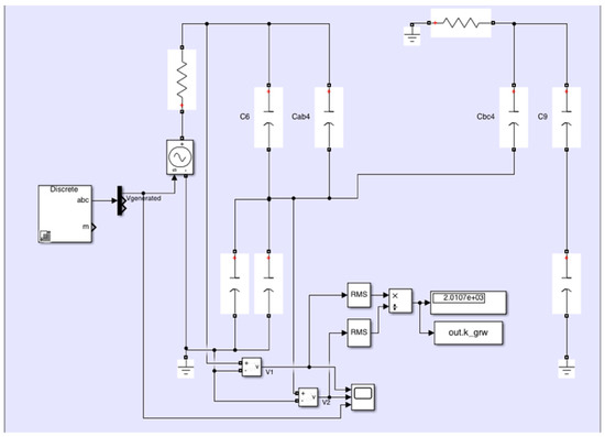
Figure 7.
Screenshot of the equivalent circuit model developed with the Simulink environment.
In addition to configurations T1–T3, which are simulated to numerically confirm the results of the circuital analysis, further configurations are implemented in the Simulink environment. Such configurations replicate experimental ones that were not used to derive the SC values but for which the ratio errors were measured. Hence, they are used as benchmarks to assess if the obtained SCs can be used to predict the ratio errors in those situations. These new configurations are referred to as T4, T5, and T6. Configuration T4 is identical to T2 but without the grounded wall W; configuration T5 instead is identical to T2 but the DD is fed with a voltage of the same amplitude but with 180° phase shift as compared with the voltage applied to the DUT. Finally, configuration T6 is identical to T5 but without the presence of the grounded wall. Furthermore, all configurations T1–T6 have been tested and simulated by applying 100%, as well as 80% of the rated voltage , as defined in [8]. This further test has been done to verify that the amplitude of the applied voltage does not affect the model of Figure 8 and the accuracy of a CD. Hence, this test confirms that the SC expressions are not influenced by the voltage amplitude, which, at the same way, does not influence the real in-lab test accuracy measurements.
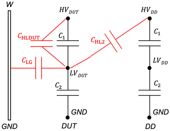
Figure 8.
The final equivalent circuit of the setup in Figure 2 including the significant SCs.
As it is clear, T4 to T6 have not been used in the computation of the SC expressions; hence, as written above, they are used for assessing their validity.
Inserting the SCs of (20) inside the model and running the simulations for T1 to T6 provides the estimated ratio errors , shown in Table 4, where the corresponding in-field measured ratio error are also reported for the sake of comparison.
Table 4.
Comparison between the measured and the estimated ratio errors.
4.3. Discussion
Several points can be highlighted from both the circuital analysis in Section 3 and the results in Table 4. The first point concerns the usefulness of the considered SCs. In fact, some SCs do not contribute to the ratio error of the CD, hence, they do not influence its accuracy. Therefore, starting from the model of Figure 3, a new and simpler model can be drawn. The model is depicted in Figure 8, and it contains, as unique contributors to the ratio error, , , and .
A second point concerns the obtained Expressions (17)–(19). Notably, by simply knowing the capacitance values of the CDs (provided on the nameplate) and the ratio errors of some test configurations, it is possible to obtain the set of SCs that identify the non-idealities of the considered circuit.
A third point concerns the simulations performed to validate the applicability of the presented expressions. As shown in Table 4, for all configuration T1–T6 and both voltage levels tested, the simulations containing the SCs obtained with Expressions (17)–(19) provide excellent results. Furthermore, what emerges from the results is that the proposed model and the obtained expressions are sufficiently accurate to describe the stray capacitance behavior in various conditions. For example, they can be used to distinguish whether or not there is a grounded wall, or if the DD is fed with an in-phase or an opposite-phase voltage. This result demonstrates the sensitivity and the effectiveness of the proposed approach.
A final point concerns the ease of applicability and usefulness of the SC expressions. In fact, the limited information required to implement the expressions and their simplicity make them an interesting and effective tool for system operators, researchers, and manufacturers. In detail, manufacturers could use the presented expressions to preliminarily test their products in order to understand whether and in which configuration they are compliant with the accuracy limits defined by the standards (see [5,6,8]) and, in the light that the considered configurations rely on that defined in [8], for assessing the immunity of CDs to external electric fields.
5. Conclusions
Stray capacitances are an undesired side effect that affect several fields and applications. They are typically treated with complex and long finite element analysis, or for very simple geometries with known equations that are not practical and flexible. Therefore, this work differs from the existing literature because it treats stray capacitance with a numerical approach that starts from a simple equivalent circuit obtained from the standards. The device, in which the stray capacitances are evaluated, is a high-voltage capacitive divider. In the work, closed expressions of the main stray capacitances are found starting from the knowledge of the ratio error of the device, measured in several configurations. The obtained expressions are evaluated with real ratio error measurements and inside a simulation environment to reproduce the real setup. All results confirm the validity and the applicability of the found expressions; furthermore, their ease of use and implementation may facilitate system operators and researchers in the study of stray capacitances of typical measurement setups. In other words, whoever is going to work with high-voltage dividers may use the proposed expressions to model its own equivalent circuit, quantifying the contribution of stray capacitances to the device accuracy.
Author Contributions
Conceptualization, L.P. and P.M.; methodology, R.T.; software, A.M. and F.C.; validation, A.M., formal analysis, R.T.; investigation, A.M.; resources, P.M.; data curation, R.T.; writing—original draft preparation, A.M. and F.C. All authors have read and agreed to the published version of the manuscript.
Funding
This research received no external funding.
Conflicts of Interest
The authors declare no conflict of interest.
References
- Available online: https://www.statista.com/statistics/873552/energy-mix-in-italy/ (accessed on 20 December 2020).
- López-Fernández, X.M.; Bülent Ertan, H.; Turowski, J. Transformers: Analysis, Design, and Measurement; CRC Press: Boca Raton, FL, USA, 2012; pp. 1–609. [Google Scholar]
- McLyman, C.W.T. Reviewing current transformers and current transducers. In Proceedings of the 2007 Electrical Insulation Conference and Electrical Manufacturing Expo, EEIC 2007, Nashville, TN, USA, 22–24 October 2007; pp. 360–365. [Google Scholar]
- Ziegler, S.; Woodward, R.C.; Iu, H.H.; Borle, L.J. Current sensing techniques: A review. IEEE Sens. J. 2009, 9, 354–376. [Google Scholar] [CrossRef]
- IEC 61869-1:2010. Instrument Transformers-Part 1: General Requirements; International Standardization Organization: Geneva, Switzerland, 2010. [Google Scholar]
- IEC 61869-6:2016. Instrument Transformers-Part 6: Additional General Requirements for Low-Power Instrument Transformers; International Standardization Organization: Geneva, Switzerland, 2016. [Google Scholar]
- IEC 61869-10:2018. Instrument Transformers-Part 10: Additional Requirements for Low-Power Passive Current Transformers; International Standardization Organization: Geneva, Switzerland, 2018. [Google Scholar]
- IEC 61869-11:2018. Instrument Transformers-Part 11: Additional Requirements for Low-Power Passive Voltage Transformers; International Standardization Organization: Geneva, Switzerland, 2018. [Google Scholar]
- Mingotti, A.; Peretto, L.; Tinarelli, R.; Ghaderi, A. Uncertainty sources analysis of a calibration system for the accuracy vs. temperature verification of voltage transformers. J. Phys. Conf. Ser. 2018, 1065, 052041. [Google Scholar] [CrossRef]
- Li, Z.; Du, Y.; Abu-Siada, A.; Li, Z.; Zhang, T. A new online temperature compensation technique for electronic instrument transformers. IEEE Access 2019, 7, 97614–97623. [Google Scholar] [CrossRef]
- Litvinov, S.N.; Lebedev, V.D.; Smirnov, N.N.; Tyutikov, V.V.; Makhsumov, I.B. Physical simulation of heat exchange between 6 kV voltage instrument transformer and its environment with natural convection and insolation. In Proceedings of the MATEC Web of Conferences, Tomsk, Russia, 24–26 April 2018; Volume 194. [Google Scholar]
- Misak, S.; Fulnecek, J. The influence of ferroresonance on a temperature of voltage transformers in undeground mines. In Proceedings of the 2017 18th International Scientific Conference on Electric Power Engineering, Kouty nad Desnou, 1 May 2017; pp. 1–4. [Google Scholar] [CrossRef]
- Sivan, V.; Robalino, D.M.; Mahajan, S.M. Measurement of temperature gradients inside a medium voltage current transformer. In Proceedings of the 2007 39th North American Power Symposium, Las Cruces, NM, USA, 30 September–2 October 2007; pp. 242–245. [Google Scholar] [CrossRef]
- Mingotti, A.; Peretto, L.; Tinarelli, R. A simple modelling procedure of rogowski coil for power systems applications. In Proceedings of the AMPS 2019-2019 10th IEEE International Workshop on Applied Measurements for Power Systems, Aachen, Germany, 25–27 September 2019; pp. 1–5. [Google Scholar] [CrossRef]
- ADadić, M.; Župan, T.; Kolar, G. FIR modeling of voltage instrument transformers from frequency response data. In Proceedings of the 2018 1st International Colloquium on Smart Grid Metrology, SmaGriMet 2018, Split, Croatia, 24–27 April 2018; pp. 1–6. [Google Scholar] [CrossRef]
- Huang, L.; Yang, W.; Zhang, X. Modeling and simulation of current transformer with air-gap based on PSCAD/EMTDC. Dianli Xitong Baohu Yu Kongzhi. Power System Prot. Control 2010, 38, 178–182. [Google Scholar]
- Nikolić, B.; Khan, S. Modelling and optimisation of design of non-conventional instrument transformers. J. Phys. Conf. Ser. 2019, 1379, 012057. [Google Scholar] [CrossRef]
- Toman, P.; Paar, M. Simulation of instrument transformer properties in power systems. In Proceedings of the 7th International Scientific Conference Electric Power Engineering, February 2006; pp. 111–115. Available online: https://www.researchgate.net/publication/290332485_Simulation_of_instrument_transformer_properties_in_power_systems (accessed on 25 February 2021).
- Torre, F.D.; Faifer, M.; Morando, A.P.; Ottoboni, R.; Cherbaucich, C.; Gentili, M.; Mazza, P. Instrument transformers: A different approach to their modeling. In Proceedings of the 2011 IEEE International Workshop on Applied Measurements for Power Systems, AMPS 2011-Proceedings 2011, Aachen, Germany, 28–30 September 2011; pp. 37–41. [Google Scholar] [CrossRef]
- Mingotti, A.; Peretto, L.; Tinarelli, R.; Zhang, J. Use of COMTRADE fault current data to test inductive current transformers. In Proceedings of the 2019 IEEE International Workshop on Metrology for Industry 4.0 and IoT, MetroInd 4.0 and IoT 2019-Proceedings, Naples, Italy, 4–6 June 2019; pp. 103–107. [Google Scholar] [CrossRef]
- Asprou, M.; Kyriakides, E.; Albu, M. The effect of instrument transformer accuracy class on the WLS state estimator accuracy. In Proceedings of the IEEE Power and Energy Society General Meeting, Vancouver, BC, Canada, 21–25 July 2013; pp. 1–5. [Google Scholar] [CrossRef]
- Draxler, K.; Styblikova, R. Calibrating an instrument voltage transformer to achieve reduced uncertainty. In Proceedings of the 2009 IEEE Intrumentation and Measurement Technology Conference, I2MTC 2009, Singapore, 5–7 May 2009; pp. 1556–1561. [Google Scholar] [CrossRef]
- Kato, H.; Imai, H. Uncertainty evaluation for the composite error of energy meter and instrument transformer. In Proceedings of the 20th IMEKO World Congress 2012, Busan, Korea, 9–14 September 2012; pp. 154–157. [Google Scholar]
- Mohns, E.; Räther, P. Test equipment and its effect on the calibration of instrument transformers. [Prüftechnik und deren Einfluss bei der Kalibrierung von Messwandlern]. Tech. Mess. 2017, 84, 91–100. [Google Scholar] [CrossRef]
- Pan, F.; Xu, Y.; Xiao, X.; Ren, S. Calibration system for electronic instrument transformers with analogue and digital outputs. In Proceedings of the ICEMI 2009-Proceedings of 9th International Conference on Electronic Measurement and Instruments 2009, Beijing, China, 16–19 August 2009; pp. 1-650–1-654. [Google Scholar] [CrossRef]
- Mingotti, A.; Peretto, L.; Tinarelli, R. Accuracy evaluation of an equivalent synchronization method for assessing the time reference in power networks. IEEE Trans. Instrum. Meas. 2018, 67, 600–606. [Google Scholar] [CrossRef]
- ACui, S.; Xue, Y.; Zhao, T.; Han, S.; Zheng, W. Research on low-temperature characteristics of the motor applied in electric vehicles. In Proceedings of the IEEE Transportation Electrification Conference and Expo, ITEC Asia-Pacific 2014-Conference Proceedings, Beijing, China, 31 August–3 September 2014; pp. 1–5. [Google Scholar] [CrossRef]
- Liwen, P.; Guangyao, L.; Yugang, D.; Chengning, Z. Electric vehicle drive-charge integrated system motor controller power loss calculation and temperature rising analysis. In Proceedings of the IEEE Transportation Electrification Conference and Expo Transportation Electrification Asia-Pacific (ITEC Asia-Pacific), Beijing, China, 31 August–3 September 2014; pp. 1–5. [Google Scholar] [CrossRef]
- Xia, Y.; Xu, Y.; Ai, M.; Liu, J. Temperature calculation of an induction motor in the starting process. IEEE Trans. Appl. Supercond. 2019, 29, 1–4. Available online: https://ieeexplore.ieee.org/document/8626507 (accessed on 25 February 2021). [CrossRef]
- Rajalakshmi, B.; Kalaivani, L. Analysis of partial discharge in underground cable joints. In Proceedings of the ICIIECS 2015-2015 IEEE International Conference on Innovations in Information, Embedded and Communication Systems, Coimbatore, India, 19–20 March 2015; pp. 1–5. [Google Scholar] [CrossRef]
- Taklaja, P.; Kiitam, I.; Hyvonen, P.; Kluss, J. Test setup for measuring medium voltage power cable and joint temperature in high current tests using thermocouples. In Proceedings of the 34th Electrical Insulation Conference, EIC 2016, Montreal, QC, Canada, 19–22 June 2016; pp. 480–483. [Google Scholar] [CrossRef]
- Zhang, L.; Yang, X.L.; Le, Y.; Yang, F.; Gan, C.; Zhang, Y. A thermal probability density-based method to detect the internal defects of power cable joints. Energies 2018, 11, 1674. [Google Scholar] [CrossRef]
- AGhaderi, A.; Mingotti, A.; Lama, F.; Peretto, L.; Tinarelli, R. Effects of temperature on mv cable joints tan delta measurements. IEEE Trans. Instrum. Meas. 2019, 68, 3892–3898. [Google Scholar] [CrossRef]
- Peretto, L.; Tinarelli, R.; Ghaderi, A.; Mingotti, A.; Mazzanti, G.; Valtorta, G.; Danesi, S. Monitoring cable current and laying environment parameters for assessing the aging rate of MV cable joint insulation. In Proceedings of the Annual Report-Conference on Electrical Insulation and Dielectric Phenomena, CEIDP 2018, Cancun, Mexico, 21–24 October 2018; pp. 390–393. [Google Scholar] [CrossRef]
- Batrakov, A.M.; Vasilev, M.Y.; Kotov, E.S.; Shtro, K.S. A precision high voltage pulse divider. Instrum. Exp. Tech. 2020, 63, 188–198. [Google Scholar] [CrossRef]
- Gao, J.; Liu, Y.; Yang, J. Design of capacitance-compensated capacitive divider for high-voltage pulse measurement. Gaodianya Jishu High Volt. Eng. 2007, 33, 76–79. [Google Scholar]
- Liu, J.; Ye, B.; Zhan, T.; Feng, J.; Zhang, J.; Wang, X. Coaxial capacitive dividers for high-voltage pulse measurements in intense electron beam accelerator with water pulse-forming line. IEEE Trans. Instrum. Meas. 2009, 58, 161–166. [Google Scholar]
- Mohns, E.; Chunyang, J.; Badura, H.; Raether, P. An active low-voltage capacitor for capacitive HV dividers. In Proceedings of the CPEM 2018-Conference on Precision Electromagnetic Measurements, Paris, France, 8–13 July 2018; pp. 1–2. [Google Scholar] [CrossRef]
- Patil, S.; Rane, M.; Bindu, S. Issues with high volatage measurement and its mitigation. In Proceedings of the 2019 4th IEEE International Conference on Recent Trends on Electronics, Information, Communication and Technology, RTEICT 2019-Proceedings 2019, Bangalore, India, 17–18 May 2019; pp. 434–438. [Google Scholar] [CrossRef]
- Riba, J.-R.; Capelli, F. Analysis of Capacitance to Ground Formulas for Different High-Voltage Electrodes. Energies 2018, 11, 1090. [Google Scholar] [CrossRef]
- Zucca, M.; Modarres, M.; Giordano, D.; Crotti, G. Accurate Numerical Modelling of MV and HV Resistive Dividers. IEEE Trans. Power Deliv. 2017, 32, 1645–1652. [Google Scholar] [CrossRef]
- Riba, J.-R.; Capelli, F.; Moreno-Eguilaz, M. Analysis and Mitigation of Stray Capacitance Effects in Resistive High-Voltage Dividers. Energies 2019, 12, 2278. [Google Scholar] [CrossRef]
- Chunting, Y.; Mingwei, W.; Caiwei, J.; Jing, Y. The stray capacitance on precision of high-voltage measurement. In Proceedings of the 2009 IEEE Instrumentation and Measurement Technology Conference, Singapore, 5–7 May 2009; pp. 249–253. [Google Scholar] [CrossRef]
- Zhu, T.; Nie, Y.; Li, Z.; Lin, X. Parameter estimation method of stray capacitance of capacitive voltage transformer based on improved particle swarm optimization algorithm. Dianli Xitong Zidonghua Autom. Electr. Power Syst. 2020, 44, 178–186. [Google Scholar]
- Dalessandro, L.; da Silveira Cavalcante, F.; Kolar, J.W. Self-Capacitance of High-Voltage Transformers. IEEE Trans. Power Electron. 2007, 22, 2081–2092. [Google Scholar] [CrossRef]
- Stanković, K.; Kovačević, U. Combined Measuring Uncertainty of Capacitive Divider with Concentrated Capacitance on High-Voltage Scale. IEEE Trans. Plasma Sci. 2018, 46, 2972–2978. [Google Scholar] [CrossRef]
- ISO/IEC JCGM 100:2008. Evaluation of Measurement Data–Guide to the Expression of Uncertainty in Measurement; International Standardization Organization: Geneva, Switzerland, 2018. [Google Scholar]


Publisher’s Note: MDPI stays neutral with regard to jurisdictional claims in published maps and institutional affiliations. |
© 2021 by the authors. Licensee MDPI, Basel, Switzerland. This article is an open access article distributed under the terms and conditions of the Creative Commons Attribution (CC BY) license (http://creativecommons.org/licenses/by/4.0/).