Abstract
This paper presents a thorough prediction of DC-link voltage switching ripples in the three-phase four-leg inverters operating in balanced and unbalanced working conditions. The unbalanced modes examined here employ the highest degree of AC current imbalance while still preserving three-phase operation. This behavior can be found in many grid-connected or standalone grid-forming three-phase converters that supply “heavy” single-phase loads, comprising a recent trend in smart-grid, smart electric vehicle (EV)-charging applications. In this sense, for instance, the smart EV chargers might be employed in conditions when different power is drawn/injected from/to the grid, providing power conditioning services to the latter. The analysis of three-phase four-leg inverters is then extended to single-phase operations typical of home-charging or vehicle-to-home (V2H) applications. Their performances in terms of DC-link voltage switching ripple are demonstrated. Two of the most common carrier-based PWM modulation techniques are employed to drive the three-phase inverter—namely, sinusoidal PWM and centered PWM (carrier-based analogy of the space vector modulation). The derived mathematical expressions of peak-to-peak and RMS values of DC-link voltage switching ripple for balanced and unbalanced conditions are handy for designing the associated DC-link capacitor and estimating the overall efficiency of the converter. Extensive numerical simulations and experimental tests have been performed to validate the presented analytical developments.
1. Introduction
Three-phase voltage-source inverters (VSIs) are widely adopted in different applications. In the case of unbalanced AC loads, four-wire topologies are employed in place of the classical three-wire inverters due to their built-in feature to handle zero-sequence components of both voltages and currents [1]. Typical applications for this kind of topology are grid-forming converters [2,3], shunt power filters [4,5], active rectifiers [6,7,8,9,10], electric drives [11], and battery chargers for electric vehicles [12,13,14]. Recently, these converters have been considered for trending smart EV chargers that are featuring vehicle-to-grid (V2G), vehicle-to-home (V2H), or even vehicle-to-vehicle (V2V) operating modes. Several configurations exist and have recently been studied in the literature, such as four-leg topologies with [15,16] and without [8,13,17] a neutral inductor, and four-wire split capacitor inverters, also with [18] and without [19] a neutral inductor.
Different modulation strategies have been proposed in the literature to control these converters—namely, space vector modulation (SVM) and carrier-based techniques. The latter are widely adopted because of their simplicity in analog and digital implementation, well-known harmonic spectrum that makes the filter design easier, and the fixed switching frequency. This last aspect is advantageous when the converter switching losses must be evaluated by simplifying the whole converter design. Among the different carrier-based PWM techniques, the sinusoidal PWM (SPWM) and the centered PWM (CPWM) are the most employed and are taken into consideration in this paper. In particular, CPWM is the SVM carrier-based equivalent [20].
As previously mentioned, a fixed switching frequency simplifies the correct design of a power switching converter and the main parameters to consider are nominal currents and voltages, and the corresponding ripples in both the AC and the DC sides. Different studies and analyses have been presented in the literature. A lot of attention has been given to the AC voltage and current characteristics. Three-phase four-leg PWM inverters are considered in [13] for evaluating the peak-to-peak and RMS of the current ripple in the three phases and in the neutral wire in case of a sinusoidal PWM technique. All these findings are helpful to estimate the main parameters for the correct design of the converter through straightforward equations. The authors of [8] optimized three-phase four-leg inverter harmonic performances by employing discontinuous PWM (DPWM) techniques.
On the other hand, considering the characteristics of the DC side, several works are presented in the literature. These analyses can help to design the DC-link capacitor properly and then the whole converter. Moreover, by employing an accurate prediction of the voltage ripple, it is possible to estimate DC-link and DC filtering stage losses and evaluate the converter’s overall efficiency. The DC-link voltage switching ripple and the DC-link capacitor’s proper design have been studied in [21] for a single-phase two-level inverter. Maximum DC-link voltage switching ripples in three-phase PWM inverters has been predicted in [22], in the case of SVM, as a function of the modulation index and phase angle. The authors of [23] investigated the DC-link voltage ripple for neutral point clamped (NPC) converter, and the RMS current of DC-link capacitors was evaluated for the same topology in [24]. Considering three-phase four-wire split capacitor inverters, DC-link voltage ripples for low order harmonics were calculated in [4,15]. A detailed analysis of positive, negative, and zero symmetric voltage components for the same topology is provided in [2]. An exhaustive study of the DC-link voltage ripple with respect to the switching frequency was given for both the total DC-link voltage and the capacitor voltages in [19]. Differently from the current manuscript, no mention of the single-phase connection typical of domestic applications (for instance, V2G/V2H) has been presented. In [25], authors have estimated the power losses in the DC-link ESR on the base of the capacitor current RMS caused by the voltage ripple. All these works highlight the importance of investigating the DC-link voltage and current characteristics.
However, to the best of the authors’ knowledge, no works provide such analysis for a three-phase four-leg PWM converter. The main novelties of this work can be summarized as follows. Firstly, the DC-link current has been calculated for both balanced and unbalanced loads. Then, the peak-to-peak DC-link voltage switching ripple has been evaluated in both cases for the sinusoidal and the centered PWM techniques. Finally, their RMS values have also been determined. The derived mathematical equations are simple and effective, and they can be used to design the DC-link capacitor properly and evaluate the whole inverter efficiency. The achieved findings are demonstrated in both simulations and experimental results.
The paper is organized as follows. In Section 2, the system configuration under analysis is presented together with the adopted modulation principles. Then, the converter DC-link current for both balanced and unbalanced phase currents is evaluated in Section 3. The next section provides the peak-to-peak and RMS voltage switching ripple analysis in both cases for sinusoidal and centered (SVM) PWM techniques and single-phase operations. Experimental results are given in Section 5 to validate the mathematical findings. Finally, conclusions are drawn in Section 6.
2. System Configuration and Modulation Principle
The four-leg topology studied here will be considered employed as an inverter in which the power is transferred from the DC side to the AC side. This is what usually happens in EV charger applications when employed in V2G and V2H operations. For this reason, the DC quantities will be indicated as “input” and the AC ones will be referred to as “output”. This choice is purely arbitrary because the voltage ripple considerations made in this manuscript are valid regardless of the power-flow direction and therefore can be straightforwardly employed in applications dealing with active rectifiers as well (for instance, grid-to-vehicle operations).
The considered three-phase four-wire four-leg inverter is depicted in Figure 1. To analyze the ripple on the DC-link capacitor (Cdc), an input impedance (Ldc and Rdc) was considered in series with the DC voltage supply (Vdc). This representation opens to the assumption that the whole switching component of the inverter input current i flows through the DC-link capacitor. On the output (ac) side, a set of three ideal sinusoidal currents indicated as ia, ib, and ic is assumed, neglecting at this stage the output current ripple.
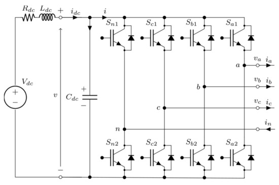
Figure 1.
Circuit scheme of a three-phase four-leg voltage-source inverter (VSI).
In the case of three-phase symmetric systems, ma = mb = mc = m, the modulating signals are obtained as the ratio between the phase reference voltages and the average of the DC-link voltage (V), as pointed out in Equation (1). Only one phase equation among the three should be considered in the case of single-phase systems.
The injected common-mode signal γ is added to the sinusoidal modulating signals ux for obtaining the actual modulating signal identified by the symbol *. Subscript x denotes the three phases, a, b, and c, and the neutral leg n. The sinusoidal components represent a three-phase symmetric system having the modulation index m as amplitude and the fundamental (grid) angular frequency ω implicitly included in the phase angle ϑ = ωt. Given the close relationship between them, the terms t (time) and ϑ will be considered interchangeable.
In this paper, common-mode signals for SPWM and CPWM are, respectively, defined by the following relation:
It is known that the CPWM technique (equivalent to SVM) extends the linear operation from m = 0.5 (i.e., the limit of SPWM) to m = 1/√3 ≅ 0.577.
In grid-connected applications, the set of grid currents, whether balanced or not, might have pretty small variation in the modulating signals of Equation (1). Indeed, as highlighted in [8,13], a small voltage unbalance can cause a considerable current unbalance. For this reason, the modulating signals can be approximated as sinusoidal and balanced waveforms if such a grid voltage is considered. In the case of a classical balanced system having a unity power factor, the set of currents can be specified as:
where Ia, Ib, and Ic are the amplitudes of output current on phase a, b, and c, respectively.
The extreme case of unbalanced currents visible in Equation (4) has been considered to extend the validity of here presented findings. The latter is the case that can happen in EV-charging applications when the Transmission System Operator (TSO) demands to drawn/inject power from/to one specific phase only rather than having the standard power sharing among the three phases.
However, it can also be the case that that the converter is connected to a single-phase grid (for instance, EV home-charging or V2H services) using two of the four available legs with a single-phase plug. In this case, there is no need to preserve an almost symmetric three-phase modulation in the detached legs. Therefore Equations (1) and (2) can, respectively, be updated (considering phase a as the sole active phase) as:
In this case, the grid current is the same reported in Equation (4). It can be argued that, when SPWM is employed, the converter behaves as a half-bridge, and therefore the maximum modulation index would be m = 0.5 (in linear operations). On the other hand, when CPWM is utilized, setting mb = mc = 0, the converter acts as an H-bridge, and the CPWM technique automatically extends the linear modulation up to m = 1. The best option is represented by the CPWM injection, which can guarantee a much broader operational range.
3. Converter DC-Link Current in Case of Balanced and Unbalanced Currents
The inverter input current i visible in Figure 1 can be seen as the summation of the phase currents that flow through upper switches. The latter statement has been reported in Equation (7) employing switching functions Sx1 equal to 1 when switches are in conduction mode and equal to 0 otherwise.
Alternatively, one can describe input current i by mean of harmonic components as:
having as the switching component at high frequency and as the input current obtained from a switching period Tsw wide rolling average. The latter is denoted by a mean value Idc at which a low-frequency component is superimposed.
The averaged input current can be calculated as:
which is both common-mode injection γ and zero-sequence current invariant.
3.1. Balanced Currents
When a three-phase set of currents is considered, Equation (9) can be updated with relations expressed in Equations (1) and (3) giving:
Moreover, if the phase currents are balanced, Equation (10) can be revised setting Ia = Ib = Ic = I and leading to the cancellation of the low-frequency component as in:
The above developments can be verified by the mean of the simulation result of Figure 2. It depicts the inverter input current i (blue trace) and its averaged component (red trace) in case of CPWM, m = 0.4, I = 1A, φ = 0°, and switching frequency fsw = 2.4 kHz. A similar profile could have been provided in the case of the SPWM technique.
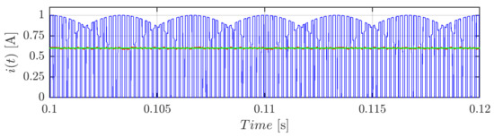
Figure 2.
Instantaneous input current i: (blue), its averaged value over the switching period (red), and calculated value (green) in case of balanced output currents centered PWM (CPWM) for m = 0.4, I = 1 A, φ = 0°, and fsw = 2.4 kHz.
As visible, the theoretical value (green trace) computed by means of Equation (11) perfectly matches with its numerical acquisition. As argued before, with being independent from the common-mode injection, the same value would have been obtained in the case of SPWM. Moreover, the input current assumes a periodicity every one-sixth of the fundamental period, and therefore its study can be restricted to a fraction of the fundamental cycle. It can be noted that, in the case of three-phase balanced currents, the sole voltage ripple component is the switching (high-frequency) one.
3.2. Unbalanced Currents
In a similar fashion to the method of the previous subsection, Equation (9) can be updated with relations expressed in Equation (4) giving:
the same result could have been obtained by replacing in Equation (10), Ib = Ic = 0 A. Equation (12) does not depend on the common-mode injection; it also does not depend on modulating signals of phases b and c. Consequently, this equation can be employed in single-phase modulation and in the case of three-phase modulation having one current only (both SPWM and CPWM techniques).
Simulation results of Figure 3a were obtained in the same conditions as Figure 2 but employing I = Ia = 1A and Ib = Ic = 0A. Figure 3b depicts the single-phase modulation counterpart (CPWM having mb = mc = 0) under the same conditions. The inverter input current i is depicted (blue trace) along with its averaged component (red trace). Again, the computation of Equation (12) (green trace) matches the numerical counterpart except for a delay due to the filtering action. Differently from the previous case, the periodicity is now equal to half of the fundamental cycle. Similar results would have been obtained utilizing three-phase SPWM.
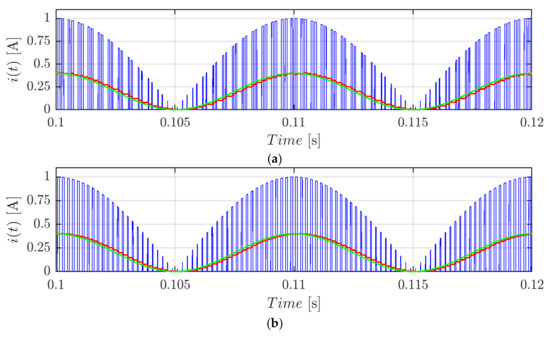
Figure 3.
Input current: instantaneous value (blue), its averaged value over the switching period (red), and calculated value (green) in case of three-phase current unbalance CPWM for m = 0.4, I = Ia = 1A, Ib = Ic = 0A (a) and single-phase modulation (b), φ = 0°, and fsw = 2.4 kHz.
The second harmonic current component causes the low-frequency voltage ripple typical of unbalanced three-phase systems [21]. On the other hand, the high-frequency component of the input current (blue traces in Figure 3) is the cause of the voltage switching ripple (studied in this paper), and it strictly depends on the employed modulation technique.
4. Evaluation of DC-Link Voltage Ripple
Similarly to Equation (8), the DC-link voltage v across the capacitor can be expressed in terms of mean value V, low-frequency averaged component , and high-frequency switching component as:
It can be argued that the mean value V differs from Vdc only for the voltage drop in the resistive component (Rdc) of the DC-link impedance. Indeed:
It is safe to assume that at the switching frequency fsw, the DC-link impedance becomes abundantly greater than the capacitive reactance, and therefore the switching current ripple component can be considered to be flowing into the DC-link capacitor only, producing the voltage switching ripple of Equation (15).
Following a similar approach to the one introduced in [19] for split-capacitor inverters, the voltage switching ripple can be computed from Equations (8) and (15) as:
which can be expressed in terms of a peak-to-peak value utilizing:
4.1. Peak-to-Peak Voltage Ripple—Balanced Currents
Taking advantage of the periodicity shown in Figure 2 when balanced currents are considered, the voltage ripple study can be restricted to the range 0 ≤ ϑ ≤ π/3. Depending on whether ia is greater or lower than Idc, two cases can be distinguished. In this regard, switching functions, current pulse disposition, and voltage ripple in the two cases ia ≥ Idc and ia < Idc have been depicted in Figure 4a and Figure 4b, respectively. The following considerations are valid for both SPWM and CPWM techniques.
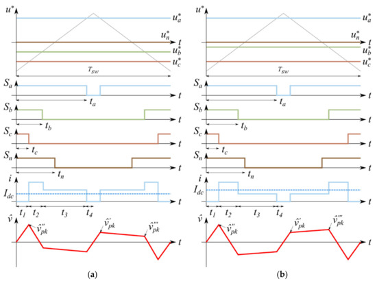
Figure 4.
Input current and DC-link voltage ripple in one switching period in case of balanced loads: (a) ia ≥ Idc, (b) ia < Idc.
The application times visible in Figure 4 can be described (for both cases) as:
which can be employed for finding pulse timings of Equation (19).
Employing the timings of Equation (19) together with the voltage ripple definition of Equation (16), the following noticeable voltage ripple peaks (depicted in Figure 4) can be found:
which defines the voltage switching ripple peak and peak-to-peak as:
4.1.1. Sinusoidal PWM
Replacing Equations (2) and (11) into Equation (20), the voltage ripple peaks in the case of SPWM can be found as:
which, if divided by I/(fsw Cdc) and inserted into Equation (21), lead to the normalized formulation () of Equation (23).
Figure 5 depicts the normalized voltage switching ripple of Equation (23) in case of SPWM, φ = 0°, and fsw = 2.4 kHz at m = 0.3 (Figure 5a) and m = 0.5 (Figure 5b). In both cases, the periodicity of the signal is every one-sixth of the fundamental period.
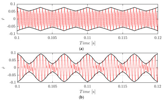
Figure 5.
Normalized DC-link voltage switching ripple (red trace) and calculated envelopes (black traces) over a period for m = 0.3 (a) and m = 0.5 (b) in case of φ = 0°, fsw = 2.4 kHz, and sinusoidal PWM (SPWM).
As already anticipated in Equation (21), both positive and negative envelopes are symmetric, and therefore the peak-to-peak value can be found by merely doubling the peak formulation of Equation (23). The peak-to-peak voltage switching ripple as a function of the modulating index m and the phase angle ϑ (with periodicity [0, π/3]) is displayed in Figure 6.
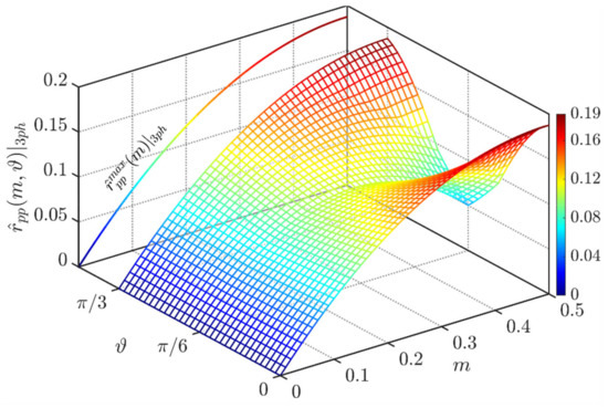
Figure 6.
Normalized peak-to-peak DC-link voltage ripple over the period [0, π/3] for SPWM and at φ = 0°.
It can be demonstrated that by replacing ϑ = 0 into Equation (23), the formulation for the maximum peak-to-peak input voltage ripple is:
Equation (24) is depicted on the left-hand side of Figure 6. As visible, the global maximum of about 0.19 p.u. appears at m = 0.5.
4.1.2. Centered PWM (SVM)
CPWM voltage ripple formulation was derived in a similar fashion to the previous subsection. As the technique denomination suggests, the pulse disposition was centered, and timings of Equation (19) t1 and t4 are equal, leading to . Indeed, replacing the common-mode injection of Equation (25) (valid in the range [0, π/3]), the voltage ripple peaks of Equation (26) can be found.
which, if divided by I/(fsw Cdc) and inserted into Equation (21), lead to the normalized formulation () of Equation (27).
Figure 7 depicts the normalized voltage switching ripple of Equation (27) in the case of CPWM at the same conditions of Figure 5. Previously stated considerations on periodicity and peak-to-peak value apply in the CPWM case as well.
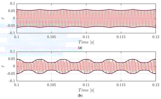
Figure 7.
Normalized DC-link voltage switching ripple (red trace) and calculated envelopes (black traces) over a period for m = 0.3 (a) and m = 0.5 (b) in case of φ = 0° and CPWM.
The peak-to-peak voltage ripple as a function of the modulating index m and the phase angle ϑ (with periodicity [0, π/3]) is depicted in Figure 8.
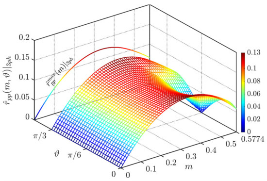
Figure 8.
Normalized peak-to-peak DC-link voltage ripple over the period [0, π/3] for CPWM and at φ = 0°.
The maximum peak-to-peak input voltage ripple has been depicted on the left-hand side of Figure 8. As visible, the global maximum of about 0.125 p.u. appears at m = 0.33.
4.2. Peak-to-Peak Voltage Ripple—Unbalanced Currents
Similar to what was conducted in the section regarding the balanced currents, pulse timings visible in Figure 9 are employed to find relevant voltage ripple peaks. As visible, phase a has been assumed as the sole active phase, having Ia = I. The findings presented here can be freely extended to other phases.
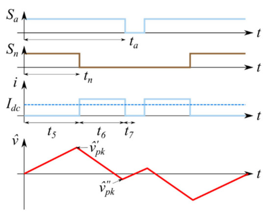
Figure 9.
Input current and voltage ripple in one switching period in case of a single-phase unbalanced load (only phase a) for ua ≥ 0.
On the basis of the application times of Equation (18), it is possible to define pulse timings regardless of the common-mode injection and the three/single-phase connection as:
The peak capacitors voltage ripples can be expressed as:
where and are called “primary” and “secondary” envelopes of capacitor voltage ripple, respectively. Although the average component of the current does not depend on the common-mode injection, timings t5 and t7 dependency from γ(ϑ) lead to different SPWM, CPWM, and single-phase modulation techniques.
4.2.1. Sinusoidal PWM
Employing Equations (6), (28), and (29), primary and secondary peaks in the case of SPWM can be defined in the whole fundamental cycle as:
which normalized traces (using the same normalization base introduced above) are depicted (black solid lines) in Figure 10 in case of m = 0.3 (Figure 10a) and m = 0.5 (Figure 10b) in case of φ = 0°. As visible, the switching ripple (solid red line) is perfectly bounded by both primary and secondary ripple within the whole fundamental period. As expected, the ripple waveform has a periodicity of half the fundamental cycle.
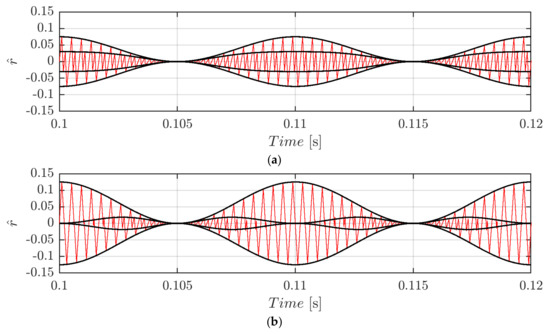
Figure 10.
Normalized DC-link voltage switching ripple (red trace) and calculated envelopes (black traces) over a period for m = 0.3 (a) and m = 0.5 (b) in case of φ = 0°, fsw = 2.4 kHz, and SPWM.
Figure 11 depicts the normalized peak-to-peak DC-link voltage ripple amplitude in the phase range ϑ = [−π/2, π/2]. It has been obtained by considering two times from the primary peak of Equation (30).
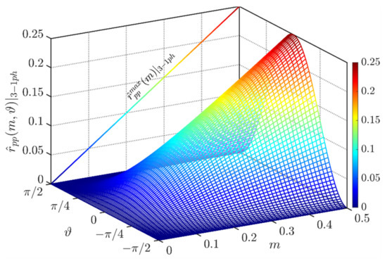
Figure 11.
Normalized peak-to-peak DC-link voltage ripple over the period [−π/2, π/2] and φ = 0° in case of SPWM.
It can be demonstrated the formulation for the maximum peak-to-peak input voltage ripple is:
Equation (31) is depicted on the left-hand side of Figure 11.
4.2.2. Centered PWM (SVM)
Taking advantage of the quarter-wave symmetry exhibited in Figure 3a, the study of the voltage ripple can be limited in the phase angle ϑ diapason [0, π/2]. In this range, the common-mode signal is:
Replacing Equations (28) and (32) into Equation (29), the voltage ripple peaks in case of CPWM becomes:
which are depicted (black traces) in normalized form in Figure 12 for the whole fundamental cycle at m = 0.3 (Figure 12a) and m = 0.4 (Figure 12b). The same set of the SPWM case has been used. Again, both envelopes perfectly match with voltage ripple profiles (red traces).
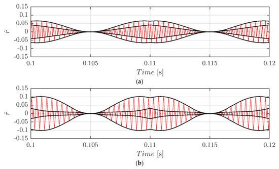
Figure 12.
Normalized DC-link voltage switching ripple (red trace) and calculated envelopes (black traces) over a period for m = 0.3 (a) and m = 0.5 (b) in case of φ = 0°, fsw = 2.4 kHz, and CPWM.
Figure 13 depicts the normalized peak-to-peak DC-link voltage ripple amplitude in the phase range ϑ = [−π/2, π/2]. It has been obtained by considering two times from the primary peak of Equation (33).
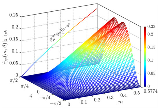
Figure 13.
Normalized peak-to-peak DC-link voltage ripple over the period [−π/2, π/2] and φ = 0° in case of CPWM.
The maximum peak-to-peak input voltage has been provided numerically in Figure 13 on the left-hand side.
4.2.3. Single-Phase Modulation
Here presented findings are carried out considering a single-phase connection employing the CPWM technique of Equation (6) having set mb = mc = 0.
Taking advantage of the half-wave symmetry exhibited in Figure 3b, the voltage ripple study can be limited in the phase angle ϑ diapason [−π/2, π/2]. In this range, the common-mode signal is:
This yields the timings t5 and t7 to be equal, suggesting coinciding envelopes (as in Section 4.1.2). Replacing Equations (28) and (34) into Equation (29), the voltage ripple peaks in the case of single-phase modulation becomes:
Equation (35) can be rearranged for obtaining the voltage ripple envelope in the whole fundamental cycle as:
which is depicted (black traces) in normalized form in Figure 14 for the whole fundamental cycle for m = 0.3 (Figure 14a) and m = 0.4 (Figure 14b). The same set of the SPWM and CPWM cases have been used. Again, both envelopes perfectly match with voltage ripple profiles (red traces).
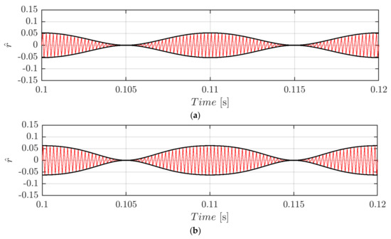
Figure 14.
Normalized DC-link voltage switching ripple (red trace) and calculated envelopes (black traces) over a period for m = 0.3 (a) and m = 0.5 (b) in case of φ = 0°, fsw = 2.4 kHz, and CPWM.
Comparing Figure 10, Figure 12, and Figure 14, one can notice that, in the case of single-phase modulation, being the two envelopes overlapped, the effect is to have a sort of switching frequency doubling that produces amplitude halving phenomenon.
Figure 15 depicts the normalized peak-to-peak DC-link voltage ripple amplitude in the phase range ϑ = [−π/2, π/2]. It has been obtained by considering two times the primary peak of Equation (35).
Figure 15.
Normalized peak-to-peak DC-link voltage ripple over the period [−π/2, π/2] and φ = 0° in case of CPWM.
The maximum peak-to-peak input voltage has been provided numerically in Figure 15 on the left-hand side. As visible, the global maximum of about 0.125 p.u. appears at m = 0.5.
4.3. Voltage Ripple RMS-Balanced Currents
Following the approach introduced in [19], it is possible to calculate the voltage ripple RMS based on the ripple waveform discussed above. As displayed in Figure 4, the voltage switching ripple assumes an irregular waveform that should be treated considering the RMS components on the piecewise function intervals. The RMS in each sector k can be seen as the composition of a DC (mean value) and AC (sawtooth/triangular-like profile) orthogonal components leading to:
Considering the contribution of each sector, the RMS on the whole switching period is calculated as follows:
which, if integrated over one-sixth of the fundamental period (due to the symmetry highlighted above), gives the final RMS formulation as:
4.3.1. Sinusoidal PWM
Employing the procedure described above, the input voltage ripple RMS in the case of SPWM can be calculated employing:
which can be normalized as:
4.3.2. Centered PWM (SVM)
Similarly, the RMS voltage ripple in the case of CPWM is:
which can be normalized as:
4.4. Voltage Ripple RMS—Unbalanced Currents
Thanks to the triangular-like waveform visible in Figure 9 (half switching period), the voltage ripple RMS in the case of one current only is evaluated based on the ripple envelopes determining its value directly on the switching period level. The DC (average) and AC (alternate) components of the RMS voltage ripples within a switching period are:
Combining both DC and AC components and integrating over [0, π/2] (thanks to the quarter-wave symmetry discussed above), the total RMS voltage ripple is derived as:
4.4.1. Sinusoidal PWM
Deriving Equation (46), the voltage ripple RMS in the case of SPWM is:
which if normalized yields:
4.4.2. Centered PWM (SVM)
The voltage ripple RMS in the case of CPWM is:
which if normalized yields:
4.4.3. Single-Phase Modulation
Similarly to Section 4.2.3., the CPWM technique reported in Equation (6) (mb = mc = 0) is considered in a single-phase connection.
Equation (44) becomes equal to zero in single-phase modulation, meaning that the RMS comes from the sole AC component due to the triangular-like waveform. The voltage ripple RMS in the case of CPWM for a single-phase load is:
which if normalized yields:
Equations (41), (43), (48), (50), and (52) representing normalized voltage ripple RMS formulations presented in this section have been depicted in Figure 16. Analytical profiles have been labeled as “theory”. On the other hand, simulation data points are displayed as “sim”. In both cases and for both injections, three-phase balanced currents are displayed as “3 ph”. Similarly, three-phase unbalanced currents (one current only) are indicated as “3-1 ph”. Finally, single-phase modulation results are labeled as “1 ph”. In all the cases, numerical results validate the analytical derivations.
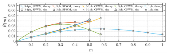
Figure 16.
Normalized RMS values of DC-link voltage ripple for studied modulation techniques and balanced/unbalanced load conditions.
As visible in Figure 16, CPWM traces outperform their SPWM counterpart over the whole modulation index range. For both “3 ph” and “3-1 ph” alternatives, SPWM and CPWM have similar performances for small values of m. Conversely, for m ≥ 0.3, the two modulation techniques detach. From trace “1 ph” performances, it is evident that, when possible, single-phase operations should be preferred if one current only is desired.
5. Experimental Results
To confirm the validity of the analytical developments introduced above, some experiments were performed on the laboratory setup, consisting of a DC source and a passive load, as shown in Figure 17a. The resulting test circuit scheme can be obtained by merging the converter circuit (Figure 1) with the passive load depicted in Figure 17b. As mentioned earlier, the designed RLC load can emulate an EV charger in V2G operation with a unity power factor.
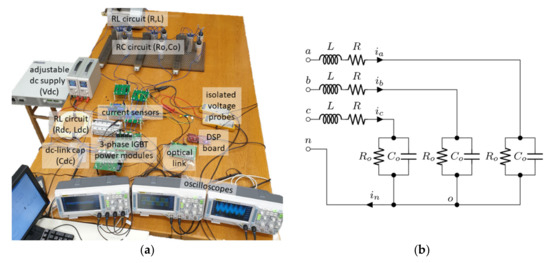
Figure 17.
(a) Experimental laboratory test bench; (b) unity power factor load.
The converter is built of four half-bridge legs formed by two IGBT-based three-phase power modules (PS22A76, 1200 V, 25 A, Mitsubishi Electric Corporation, Tokyo, Japan). The DC side of the VSC is linked with an adjustable DC power supply (GEN100-33, 100 V, 33 A, TDK-Lambda Corporation, Tokyo, Japan) through a DC-link capacitor (Cdc) and the RL input series circuit (Rdc, Ldc). The input inductance serves to form the input voltage ripple path passing solely through the DC-link capacitor. The converter is connected to an induction motor (2.2 kW, 400 V) on the AC side, representing the RL load series circuit. For this experiment, a relatively high inductance is required to minimize disruptive AC current ripple on the AC side. However, the effect of frequency-driven inductance variation in induction motors should be taken into account [26]. In this case, inductance at the switching frequency is lower than the value at the fundamental frequency. Since this paper aims to report voltage switching ripple, it is important to obtain an AC output current that is as clean as possible from the corresponding switching current ripple. In addition to the large interface AC inductance, a slightly higher value of switching frequency was applied to mitigate AC current ripple’s detrimental effect. The RC load parallel circuit was obtained by the parallel connection of an AC capacitor and resistor in each phase (cf. Figure 17b). For wiring simplicity in the laboratory setup, the RL series circuit (the induction motor) was swapped with RC parallel circuit (cf. Figure 17a,b). This modification does not introduce any change in the equivalent circuit illustrated in Figure 17b. All the circuital parameters are summarized in Table 1. Currents and voltages measurements were performed by employing current sensors (LA 55-P, LEM Europe GmbH, Fribourg, Switzerland) and isolated differential voltage probes (PICO TA057, Pico, Tyler, TX, USA), respectively. The converter legs were driven by a DSP board (TMS320 F28379D, Texas Instruments, Dallas, TX, USA) via isolated intermediate optical links. The modulation characteristics were regulated in an open-loop via real-time MATLAB/Simulink (MathWorks, Natick, MA, USA) platform in the external mode. The measured data samples have been acquired using digital oscilloscopes (DS1054Z, Rigol, Beijing, China) with a sampling frequency of 5 MHz. The results were plotted via MATLAB, without additional pre-filtering, unless otherwise specified.

Table 1.
Setup parameters.
The amplitude of the AC current I is directly proportional to the modulation index m, according to:
where v and Zeq are the voltage of the DC supply minus voltage drop due to RL input circuit (cf. Figure 1) and the unity power factor load impedance, respectively. With reference to Table 1, Zeq ≅ 18.8 Ω.
Since the focus is drawn to the grid-connected applications in this paper, only some experimental results associated with high values of the modulating index range are demonstrated.
Figure 18 and Figure 19 depict the DC-link voltage ripple for three-phase VSI arrangement with balanced currents and two examined modulation schemes, SPWM and CPWM. To obtain only high-frequency (switching) components of the voltage ripple, the measured waveform was prefiltered using a bandpass filter with bandwidth from 1 to 50 kHz. Both figures illustrate two subcases at m = 0.3 (a) and m = 0.5 (b). As can be seen, the acquired ripple measurements reasonably match with the analytical envelopes calculated by Equation (23) for SPWM and Equation (27) for CPWM, taking into account the scaling factor I/(fsw Cdc) and the amplitude of the AC current I discussed in Equation (53). It is also interesting to note the frequency doubling effect in Figure 19 with respect to the voltage ripples at similar modulating indices in Figure 18. As was discussed in Section 4.2.3, this happens since primary and secondary ripples have similar magnitudes. The time range in the experimental plots is preserved in terms of how data were acquired. Namely, timing “0” represents the triggering time instant. Simultaneously, the negative and positive diapasons denote the time spans before and after the triggering moment, respectively.
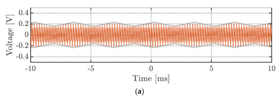
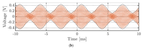
Figure 18.
DC-link voltage switching ripple, operating in the balanced currents mode under SPWM and at: (a) m = 0.3; (b) m = 0.5.
Figure 19.
DC-link voltage switching ripple, operating in the balanced currents mode under CPWM and at: (a) m = 0.3; (b) m = 0.5.
Similarly, the RMS value of the DC voltage ripple can be obtained. Strictly speaking, one should introduce the amplitude of the AC current I from Equation (53) into Equation (40) for SPWM and into Equation (42) for CPWM modulation cases.
An excellent correlation of the theoretical RMS voltage ripple profile with the measured RMS values can be observed in Figure 20. However, one may notice a slight mismatch of the experimental values at a low range of modulating indices. This fact can be explained by the prevalence of measuring noise and higher uncertainties at lower voltage ranges. Overall, the depicted experimental results confirm the presented development’s validity for the balanced three-phase load/grid operation.
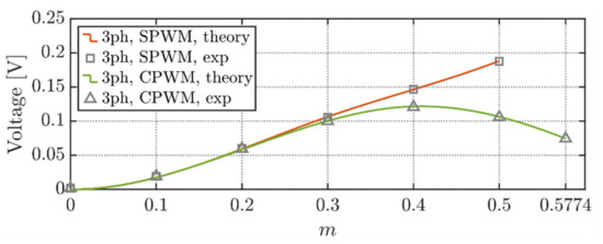
Figure 20.
RMS value of DC-link voltage switching ripple for the balanced three-phase currents condition under SPWM and CPWM.
The above considerations are highlighted again in the absolute and relative error assessment in Table 2. Although the absolute error appears to be restrained in the whole modulating index range, the noise’s effect is particularly detrimental in low-ripple working points (m < 0.2), where the relative error rises above 1%.
Table 2.
Voltage ripple RMS error evaluation for the balanced three-phase currents condition under SPWM and CPWM.
For the sake of completeness, the AC current and phase voltage are depicted in Figure 21. As visible from Figure 21a, a set of balanced sinusoidal phase currents has been obtained with a small residual switching current ripple. The harmonic content of the associated phase current (ph. a) is shown in Figure 21b. On the other hand, Figure 21c shows the phase voltage having an identical phase angle with a fundamental component of the corresponding phase current, validating the unity power factor operation.
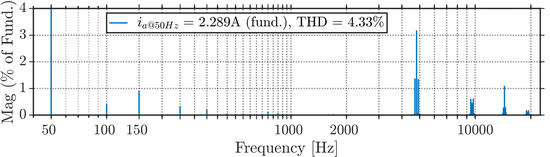
Figure 21.
(a) Balanced phase currents (@ m = 0.5); (b) harmonic spectrum of a phase current (phase a, @ m = 0.5); (c) phase output voltage (phase a, blue trace) and its fundamental component (purple trace) in comparison with phase current (@ m = 0.5, red trace).
Figure 22 demonstrates the DC voltage ripple (red traces) and its wrapping envelopes (black traces) measured under an unbalanced single-phase. The figure presents voltage switching ripple at m = 0.5. To obtain only high-frequency (switching) components of the voltage ripple, the measured waveform was prefiltered using a bandpass filter with a bandwidth from 1 to 50 kHz. It can be noted that primary and secondary ripple envelopes overlap with one another. Therefore, the frequency doubling effect can be observed here as well. Although the derived envelopes nicely bound the measured voltage ripple, the residual noise presence is evident. For low voltage ripple values (when the envelopes get close to zero), the measuring noise and uncertainties become predominant and start to interfere with the ripple. Compared to previous experimental plots, this phenomenon is more evident due to the small magnitude of the voltage ripple in single-phase modulation.
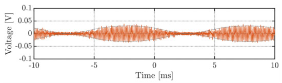
Figure 22.
DC-link voltage switching ripple, operating in the single-phase modulation at m = 0.5.
Figure 23 validates theoretical equations presented in Section 4.4 regarding RMS voltage ripple for the single-phase modulation. The results are depicted for the whole linear modulation range m ∈ [0, 1]. Differently from numerical verifications, at low modulation indices, the measuring noise and associated uncertainties dominate the voltage ripple in the whole fundamental cycle, causing an inevitable mismatch of experimental data points with the analytically derived trace.
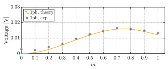
Figure 23.
RMS value of DC-link voltage switching ripple for the single-phase modulation.
In a similar fashion to Table 2, a single-phase modulation error assessment is presented in Table 3. Overall, the absolute error appears to have the same order of magnitude as the one shown in Table 2. However, the relative error is noticeable worsened due to the single-phase modulation voltage ripple’s lower magnitude.
Table 3.
Voltage ripple RMS error evaluation for the single-phase modulation.
Overall, experimental results validate the analytical findings and reasonably match the numerical results, ensuring the proposed development’s accuracy.
6. Conclusions
Instantaneous DC-link voltage ripples in three-phase four-leg PWM inverters have been analyzed in this paper. The prediction presented here permits the analytically derivation of the peak-to-peak, maximum, and the RMS of the DC-link voltage switching ripple. Multiple real-world working modes, such as three-phase connection with balanced currents, three-phase connection with single-phase power absorption, and single-phase connection, have been considered and validated numerically and experimentally. A possible application can be easily found in the EV-charging context where different connections/plugs and transmission system operator dispatch orders can be found. Furthermore, the DC-link voltage switching ripple’s prediction is useful in designing the DC-link capacitor and the DC filtering stage to prevent harmonic pollution and mitigate electromagnetic interferences. Additionally, it can also be used to estimate converter overall efficiency and aging of capacitors.
In the case of three-phase connections, the CPWM (SVM) technique should always be preferred. In particular, in the case of a balanced absorption, the RMS value of the voltage ripple might be up to 43% lower than the SPWM counterpart. On the other hand, if the power is drawn/injected from one phase only, the benefit of CPWM is limited to a maximum voltage ripple RMS reduction of about 12%. Concerning single-phase applications, the operating range can almost double, preserving a voltage switching ripple harmonic content in the same range magnitude experienced by the three-phase one. Similar considerations concerning the voltage ripple peak-to-peak maximum value can be taken into account.
Experimental results have been provided to validate the achieved analytical findings on a four-leg converter employed in three-phase and single-phase (V2G/V2H) connection modes. It has been demonstrated that the obtained results adequately match the predicted DC voltage switching ripple. The attained relative error is within 1% for three-phase connections and within 10% for their single-phase counterparts in the most popular working conditions (i.e., m ≥ 0.4 and m ≥ 0.8, respectively).
Future studies might enlarge the prediction proposed here by taking discontinuous PWM techniques into consideration as well. Moreover, variable switching frequency PWM techniques aiming to mitigate DC-link voltage ripple could be developed based on the voltage ripple envelopes prediction carried out here.
Author Contributions
Conceptualization, R.M., A.V., and M.H.; methodology, R.M., A.V., M.H., and G.G.; software, A.V. and M.H.; validation, R.M., A.V., and M.H.; formal analysis, R.M. and M.H.; investigation, R.M., A.V., and M.H.; resources, R.M., A.V., and M.R.; data curation, R.M., A.V., and M.H.; writing—original draft preparation, R.M., A.V., M.H., and M.R.; writing—review and editing, R.M., A.V., M.H., M.R., and G.G.; visualization, A.V. and M.H.; supervision, M.R. and G.G. All authors have read and agreed to the published version of the manuscript.
Funding
This research received no external funding.
Institutional Review Board Statement
Not applicable.
Informed Consent Statement
Not applicable.
Data Availability Statement
Data are available in the document.
Conflicts of Interest
The authors declare no conflict of interest.
Nomenclature
| x | Index for phases a, b, c, and neutral n, used as a subscript |
| , | Converter’s instantaneous phase current and its amplitude |
| ,,,, | Converter’s input current instantaneous value, high-frequency component, low-frequency component, averaged component, and mean value |
| ,,,, | Converter’s DC-link voltage instantaneous value, high-frequency component, low-frequency component, averaged component, and mean value |
| , | Modulating signals and sinusoidal modulating signal |
| γ | Common-mode injection |
| mx, m | Modulation index (normalized by DC-link voltage Vdc) |
| ϑ, t | Phase angle and time |
| Sx1 | Legs’ switching functions |
| , | Peak (pk) and peak-to-peak (pp) voltage ripple wrapping envelopes |
| , | Normalized peak (pk) and peak-to-peak (pp) voltage ripple wrapping envelopes |
| , | Maximum peak-to-peak input voltage ripple and its normalization |
| , | DC-link voltage switching ripple RMS and its normalization |
References
- Zhao, W.; Ruan, X.; Yang, D.; Chen, X.; Jia, L. Neutral Point Voltage Ripple Suppression for a Three-Phase Four-Wire Inverter With an Independently Controlled Neutral Module. IEEE Trans. Ind. Electron. 2017, 64, 2608–2619. [Google Scholar] [CrossRef]
- Nascimento, C.F.; Diene, O.; Watanabe, E.H. Analytical Model of Three-Phase Four-Wire VSC Operating as Grid Forming Power Converter under Unbalanced Load Conditions. In Proceedings of the 2017 IEEE 12th International Conference on Power Electronics and Drive Systems (PEDS), Honolulu, HI, USA, 12–15 December 2017; pp. 1219–1224. [Google Scholar]
- Carrasco, G.; Silva, C.A.; Peña, R.; Cárdenas, R. Control of a Four-Leg Converter for the Operation of a DFIG Feeding Stand-Alone Unbalanced Loads. IEEE Trans. Ind. Electron. 2015, 62, 4630–4640. [Google Scholar] [CrossRef]
- Khadkikar, V.; Chandra, A.; Singh, B. Digital signal processor implementation and performance evaluation of split capacitor, four-leg and three H-bridge-based three-phase four-wire shunt active filters. IET Power Electron. 2011, 4, 463–470. [Google Scholar] [CrossRef]
- Aredes, M.; Hafner, J.; Heumann, K. Three-Phase Four-Wire Shunt Active Filter Control Strategies. IEEE Trans. Power Electron. 1997, 12, 311–318. [Google Scholar] [CrossRef]
- Yaramasu, V.; Rivera, M.; Wu, B.; Rodriguez, J. Model Predictive Current Control of Two-Level Four-Leg Inverters—Part I: Concept, Algorithm, and Simulation Analysis. IEEE Trans. Power Electron. 2013, 28, 3459–3468. [Google Scholar] [CrossRef]
- Rivera, M.; Yaramasu, V.; Rodriguez, J.; Wu, B. Model Predictive Current Control of Two-Level Four-Leg Inverters—Part II: Experimental Implementation and Validation. IEEE Trans. Power Electron. 2013, 28, 3469–3478. [Google Scholar] [CrossRef]
- Mandrioli, R.; Viatkin, A.; Hammami, M.; Ricco, M.; Grandi, G. A Comprehensive AC Current Ripple Analysis and Performance Enhancement via Discontinuous PWM in Three-Phase Four-Leg Grid-Connected Inverters. Energies 2020, 13, 4352. [Google Scholar] [CrossRef]
- Dorf, R.C.; Bishop, R.H. Modern Control Systems, 11th ed.; Prentice Hall: Upper Saddle River, NJ, USA, 2008. [Google Scholar]
- Ghosh, R.; Narayanan, G. Control of Three-Phase, Four-Wire PWM Rectifier. IEEE Trans. Power Electron. 2008, 23, 96–106. [Google Scholar] [CrossRef]
- Li, A.; Jiang, D.; Kong, W.; Qu, R. Four-Leg Converter for Reluctance Machine With DC-Biased Sinusoidal Winding Current. IEEE Trans. Power Electron. 2019, 34, 4569–4580. [Google Scholar] [CrossRef]
- Fu, Y.; Li, Y.; Huang, Y.; Lu, X.; Zou, K.; Chen, C.; Bai, H. Imbalanced Load Regulation Based on Virtual Resistance of A Three-Phase Four-Wire Inverter for EV Vehicle-to-Home Applications. IEEE Trans. Transp. Electrif. 2019, 5, 162–173. [Google Scholar] [CrossRef]
- Viatkin, A.; Mandrioli, R.; Hammami, M.; Ricco, M.; Grandi, G. AC Current Ripple Harmonic Pollution in Three-Phase Four-Leg Active Front-End AC/DC Converter for On-Board EV Chargers. Electronics 2021, 10, 116. [Google Scholar] [CrossRef]
- Fu, Y.; Li, Y.; Huang, Y.; Bai, H.; Zou, K.; Lu, X.; Chen, C. Design Methodology of a Three-Phase Four-Wire EV Charger Operated at the Autonomous Mode. IEEE Trans. Transp. Electrif. 2019, 5, 1169–1181. [Google Scholar] [CrossRef]
- Hintz, A.; Prasanna, R.; Rajashekara, K. Comparative Study of Three-phase Grid Connected Inverter Sharing Unbalanced Three-phase and/or Single-phase systems. In Proceedings of the 2015 IEEE Energy Conversion Congress and Exposition (ECCE), Montreal, QC, Canada, 20–24 September 2015; pp. 6491–6496. [Google Scholar]
- Hintz, A.; Prasanna, U.R.; Rajashekara, K. Comparative Study of the Three-Phase Grid-Connected Inverter Sharing Unbalanced Three-Phase and/or Single-Phase systems. IEEE Trans. Ind. Appl. 2016, 52, 5156–5164. [Google Scholar] [CrossRef]
- Kim, J.-H.; Sul, S.-K. A Carrier-Based PWM Method for Three-Phase Four-Leg Voltage Source Converters. IEEE Trans. Power Electron. 2004, 19, 66–75. [Google Scholar] [CrossRef]
- Lin, Z.; Ruan, X.; Jia, L.; Zhao, W.; Liu, H.; Rao, P. Optimized Design of the Neutral Inductor and Filter Inductors in Three-Phase Four-Wire Inverter With Split DC-Link Capacitors. IEEE Trans. Power Electron. 2019, 34, 247–262. [Google Scholar] [CrossRef]
- Hammami, M.; Mandrioli, R.; Viatkin, A.; Ricco, M.; Grandi, G. Analysis of Input Voltage Switching Ripple in Three-Phase Four-Wire Split Capacitor PWM Inverters. Energies 2020, 13, 5076. [Google Scholar] [CrossRef]
- Hava, A.M.; Kerkman, R.J.; Lipo, T.A. Carrier-based PWM-VSI overmodulation strategies: Analysis, comparison, and design. IEEE Trans. Power Electron. 1998, 13, 674–689. [Google Scholar] [CrossRef]
- Vujacic, M.; Hammami, M.; Srndovic, M.; Grandi, G. Theoretical and Experimental Investigation of Switching Ripple in the DC-Link Voltage of Single-Phase H-Bridge PWM Inverters. Energies 2017, 10, 1189. [Google Scholar] [CrossRef]
- Vujacic, M.; Hammami, M.; Srndovic, M.; Grandi, G. Analysis of dc-link voltage switching ripple in three-phase PWM inverters. Energies 2018, 11, 471. [Google Scholar] [CrossRef]
- Hammami, M.; Rizzoli, G.; Mandrioli, R.; Grandi, G. Capacitors Voltage Switching Ripple in Three-Phase Three-Level Neutral Point Clamped Inverters with Self-Balancing Carrier-Based Modulation. Energies 2018, 11, 3244. [Google Scholar] [CrossRef]
- Gopalakrishnan, K.S.; Das, S.; Narayanan, G. Analytical expression for RMS DC link capacitor current in a three-level inverter. In Proceedings of the Centenary Conference Electrical Engineering, Indian Institute of Science, Bangalore, India, 15–17 December 2011; pp. 1–6. [Google Scholar]
- Chen, T.; Li, S.; Fahimi, B. Analysis of DC-Link Voltage Ripple in Voltage Source Inverters without Electrolytic Capacitor. In Proceedings of the IECON 2018—44th Annual Conference of the IEEE Industrial Electronics Society, Washington, DC, USA, 21–23 October 2018; pp. 1041–1048. [Google Scholar]
- Srndovic, M.; Fišer, R.; Grandi, G. Analysis of Equivalent Inductance of Three-phase Induction Motors in the Switching Frequency Range. Electronics 2019, 8, 120. [Google Scholar] [CrossRef]


Publisher’s Note: MDPI stays neutral with regard to jurisdictional claims in published maps and institutional affiliations. |
© 2021 by the authors. Licensee MDPI, Basel, Switzerland. This article is an open access article distributed under the terms and conditions of the Creative Commons Attribution (CC BY) license (http://creativecommons.org/licenses/by/4.0/).