Article

Input Parallel Output Series Structure of Planar Medium Frequency Transformers for 200 kW Power Converter: Model and Parameters Evaluation

Politecnico di Torino, Department of Energy, Corso Duca degli Abruzzi 24, 10129 Torino, Italy
*
Author to whom correspondence should be addressed.
Energies 2021, 14(5), 1450; https://doi.org/10.3390/en14051450
Submission received: 14 January 2021 / Revised: 12 February 2021 / Accepted: 1 March 2021 / Published: 7 March 2021
(This article belongs to the Special Issue Power Converters: Modeling, Design and Applications)

Abstract

:
Nowadays, the demand for high power converters for DC applications, such as renewable sources or ultra-fast chargers for electric vehicles, is constantly growing. Galvanic isolation is mandatory in most of these applications. In this context, the Solid State Transformer (SST) converter plays a fundamental role. The adoption of the Medium Frequency Transformers (MFT) guarantees galvanic isolation in addition to high performance in reduced size. In the present paper, a multi MFT structure is proposed as a solution to improve the power density and the modularity of the system. Starting from 20 kW planar transformer model, experimentally validated, a multi-transformer structure is analyzed. After an analytical treatment of the Input Parallel Output Series (IPOS) structure, an equivalent electrical model of a 200 kW IPOS (made by 10 MFTs) is introduced. The model is validated by experimental measurements and tests.

1. Introduction

Power converter topologies can be classified into two main categories: isolated converters and non-isolated converters. Isolated converters like Solid State Transformers (SST) use the Medium Frequency Transformer (MFT) to guarantee galvanic isolation. The use of an MFT implies the use of devices capable to switch at high frequencies, such as the Wide Band Gap (WBG) ones. The most common WBGs are unipolar transistors based on Gallium Nitride (GaN) and Silicon Carbide (SiC) semiconductor technology. From one side, the WBG components can switch at high frequencies, on the other side they have some disadvantages. Their fast switching capability results in high dV/dt during transitions, this can cause overvoltages in electrical drives with long connections between the converter and the load [1]. Overvoltage problems can be mitigated by reducing the voltage rising edges (dV/dt) in switching through the driving circuits (actively) or passively [2]. High dV/dt values can excite resonances at high frequencies leading to EMI issues. Thus, the spectral modeling of the MFT becomes fundamental for the identification of the switching limits into SST converters.
Based on design data such as currents, voltages, frequency, and flux density, it is possible to perform a comparison between axial and planar transformers [3]. Due to their flat shape, planar MFTs present advantages in term of heat dissipation compared to axial MFT [4]. In [5], it is shown that a planar MFT adopting interleaving between layers presents a lower leakage inductance than an axial MFT.
Over the past few decades many studies have been carried out on the identification of valid models for MFTs especially for low power and medium frequency applications (till GHz frequency range applications) [6]. Finite Element Analysis (FEA) method can be adopted to analyze inductive parameters such as the leakage inductance of MFT [7,8], even for high voltage applications [9]. Some models include the effects of iron and copper losses [10,11,12]. In medium frequencies ( 100 kHz till 50 MHz ) also capacitive parasitisms must be considered [13,14].
In planar MFTs, interleaving, core shape [15], and power switches parasitic capacitance [16] introduce Common Mode (CM) paths. To reduce capacitive phenomena, some studies propose a shielding between layers [17] or the introduction of an out of phase turn layer into the winding of the planar MFT [18,19,20]. It has been shown that the CM noise is similar between axial and planar MFTs [21]. An indicator for the CM noise filtering is given by the ratio between leakage inductance and parasitic capacitance ( L lk / C p ), by increasing this ratio, the system can filter common mode currents more effectively [22]. A good design is based on the trade-off between the values of leakage inductance and parasitic capacitance.
For Medium Frequency and 200 kW applications, state-of-the-art are the single-phase axial transformers [23]. Despite the axial transformers, the high reproducibility with a low dispersion of the electrical parameters is a planar transformers advantage. A stack of low power planar MFTs, as proposed in this paper, can be a competitive solution indeed. The stack helps to contain the transformer’s size and to increase the power rate of the system. A stack of MFTs, having the same parameters, can be connected in several configurations.
In electrical power transmission, the typical connection to increase the power is the parallel one. The series connection among a certain number of transformers reduces the voltage at each transformer terminal keeping the same voltage ratio. This solution is not typically adopted. The combination of series and parallel connections can be interesting for applications with an SST converter. An Input Series Output Parallel (ISOP) configuration have been presented in [24]. The present paper proposes an Input Parallel Output Series (IPOS) connection for a 200 kW SST converter adopting 10 planar MFTs.
The reason to chose the IPOS configuration is related to the system specification. The 200 kW SST converter needs a transformer with a primary to secondary voltage ratio t equal to one (1:1). A 200 kW planar transformer with 1:1 ratio is a device in which the parasitic capacitance effects are significant. To compensate the parasitic phenomena in the planar transformer, the number of turns on the two transformer side is different; thus, t is more than 1. In this paper, the single MFT has a voltage ratio equal to 10 and a power rate of 20 kW .
This paper is arranged as follows: in Section 3, the principal MFTs models are presented, one of them is chosen for the adopted 20 kW planar transformers. In Section 4, the model of an IPOS structure consisting of generic number N of transformers is derived. The model composed of 2, 5, 6, and 10 MFTs is then experimentally validated in Section 5 by LC measuring. Finally, in Section 5.2, power tests illustrate the effectiveness of the IPOS-10 in SST power converters.

2. High Frequency Planar Transformers Models

This section presents the main models for high frequency transformers for power electronics applications. A valid model for these applications must include the inductive and capacitive components of the HFT. The models mostly used are shown in Figure 1. The frequency response of these models can be assessed through their transfer functions [25].
The inductive behavior is modeled through connected elements both in the series branch and in the parallel branch of the HFT model. The series connected elements are the leakage inductance at the primary ( L lk 1 ) and secondary ( L lk 2 ) sides. The series parameter are affected by winding interleaving, copper, and insulator thickness. Adding an out of phase half turn to the winding or parallelizing more turns of the same winding [7] affects these parameters. Ref. [12] carried out a calculation of leakage inductance and series resistance in planar magnetics, comparing an interleaved and not interleaved winding. The study shows that there are no substantial differences between the two cases for frequencies below 100 kHz .
The parallel connected element is the magnetize inductance ( L m ). This parameter depends on core material and geometry. Leakage and magnetize inductance can be evaluated through optimization methods [8], calculated analytically or through experimental measurements. Experimental measurements can be made using an LCR meter. Two measurements are usually taken: open circuit measurement (Figure 2a) and short circuit measurement (Figure 2b). Capacitive parameters can also be evaluated analytically [26] through FEA simulations or through experimental measurements [27]. One of the analytical methods is based on the calculation of parasitic capacities through the evaluation of the electrostatic energy stored in the insulation between the windings. Refs. [13,28] adopt this calculation for the six-capacitance model (Figure 1c). The stored energy in a six capacitance model of an high frequency transformer can be defined as:
W E = 1 2 C p V 1 2 + 1 2 C s V 2 2 + 1 2 C ps 1 V 3 2 + 1 2 C ps 2 ( V 1 V 2 V 3 ) 2 + + 1 2 C ps 3 ( V 2 + V 3 ) 2 + 1 2 C ps 4 ( V 1 V 3 ) 2
where V 1 , V 2 , V 3 are, respectively, the voltage at the primary side, the voltage at the secondary side, and the voltage between primary and secondary voltage. The equivalent parallel capacitance can be defined by means the other equivalent capacitance:
C p = c 11 c 13 ; C s = c 22 c 23 ; C ps 1 = c 33 + c 13 c 12 c 23 C ps 2 = c 12 ; C ps 3 = c 12 + c 23 ; C ps 4 = c 12 c 13
where
c 11 = 1 3 C 0 ; c 22 = 1 3 C 0 ; c 33 = C 0 ; c 12 = 1 3 C 0 ; c 23 = 1 2 C 0 ; c 13 = 1 2 C 0
In which C 0 is the capacitance between two adjacent layers. In [29] is carried out the effectiveness of the six capacitance model evaluated on axial transformer. However, the model must be applied only between layers belonging to different winding. For layers belonging to the same winding, the capacitance is equal to C 11 = 1 3 C 0 . Even the three (Figure 1b and single Figure 1a) capacitance models can be obtained through experimental measurements. In [30], experimental validation on a 500 W , 25 kHz transformer is performed. This study proposes the follow equation for the capacitance’s evaluation:
C p = C p 0 + ( 1 t ) C ps 0
C s = k 2 C s 0 + t ( t 1 ) C ps 0
C ps = t C ps 0
where C p is the capacitance at the primary side, C s the capacitance at the secondary, and C ps is the capacitance between primary and secondary sides. C p 0 is the stray capacitance measured at primary side with the secondary side in open circuit conditions (Figure 2a), C s 0 is the secondary stray capacitance measured when the primary side is in open circuit conditions, and C ps 0 is the stray capacitance between primary and secondary sides (Figure 2c).
The measurements must be made in a frequency range that includes harmonics higher than the switching frequency as in [31], where the measurements were made up to 500 kHz, but with the use of the WBG devices this limit could be moved higher.
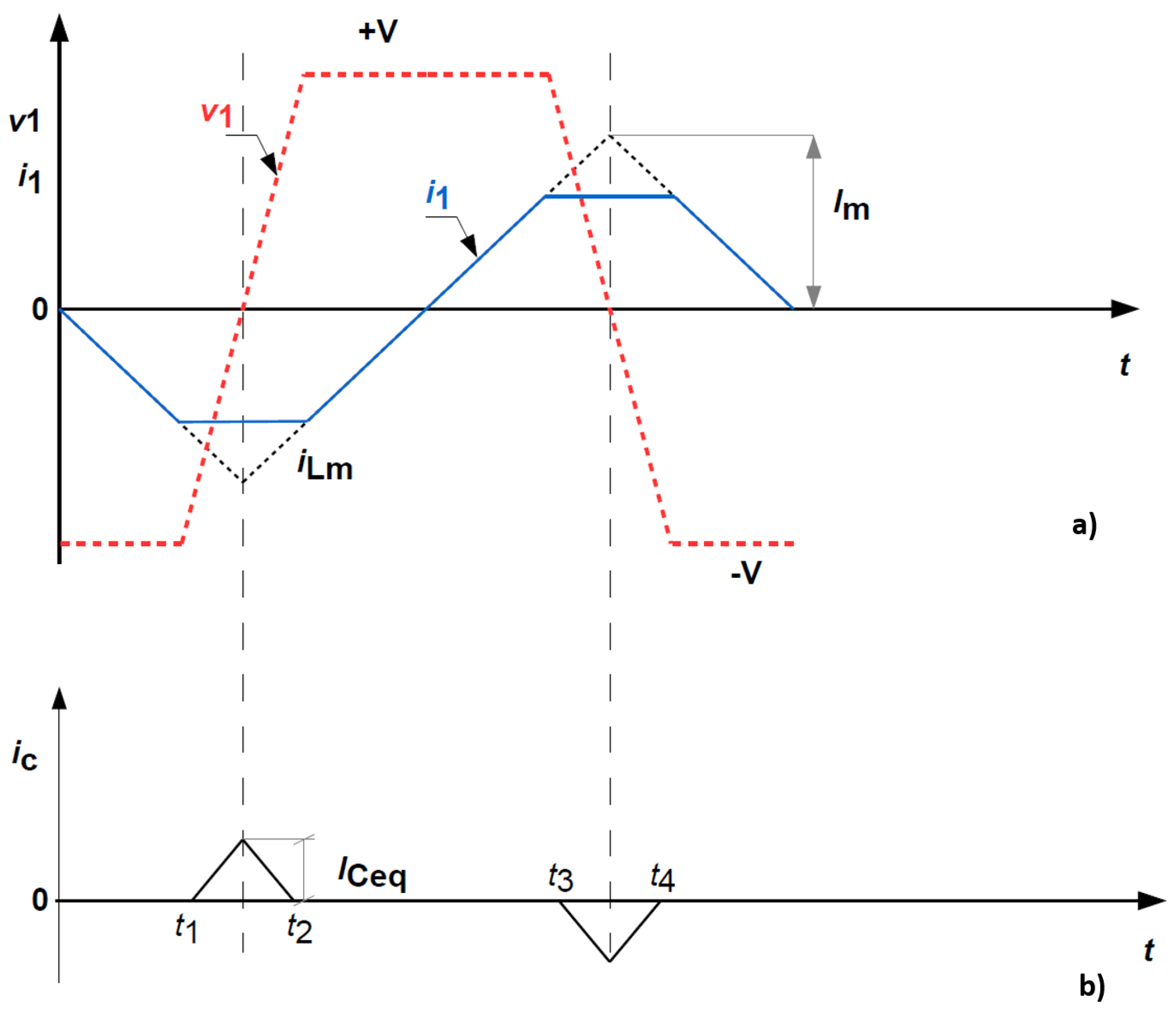
A closed loop equation for the three capacitance model (Figure 1b) based on LCR measurement is provided by [32]. C s is the capacitance of the secondary side view from the primary side. f 1 , f 2 , and f 3 are the resonance frequency of the bode diagram. Another experimental method for the evaluation of the parasitic capacitance in an HFT is to supply the Device Under Test (DUT) adopting a DC/AC converter. Applying square wave voltage to the HFT in open circuit conditions, the magnetized current passes through the primary winding. Ideally, magnetizing the current is a triangular waveform; in practice, holes on the peaks of the triangular current waveform appear. These are due to the effects of parasitic capacitances excited by the high dV/dt values during commutations (Figure 3).
Analytically, the voltage applied to the stray capacitance can be defined as:
V Ceq = 1 C eq i Ceq d t
The amount of charge displaced in the equivalent parasitic capacity is equal to the integral of the current in the switching time.
Q Ceq = i Ceq d t
From Figure 3b, it can be seen that the result of the integral is the area of the triangle having the switching time as the basis and the current variation during switching as the height. Substituting (10) in (9), the equivalent capacitance can be calculated. Due to the complexity of the proposed ISOP structure, the simplest model (Figure 1a) has been chosen after a step of experimental validation.

Experimental Validation of HFT Models

In order to define a model of a multi-transformer structure, it is necessary to have a valid model of the single HFT. The experimental tests aim to validate a single capacity model of an HFT (Figure 1a). The DUT is a 20 kW planar transformer with a 10:1 transformation ratio. The working frequency of the DUT can vary between 40 kHz and 1 MHz . The parameters are obtained through measurements made with an LCR meter (Hioki-IM3536). The measuring terminals are compensated to be able to carry out frequency measurements up to 8 MHz . The connections made during the tests are shown in Figure 2. In particular, the open circuit measurement (Figure 2a) allows to obtain the parameters in parallel: C p and L m . The short circuit measurement is carried out to derive the series parameters of the model: L lk 1 and L lk 2 .
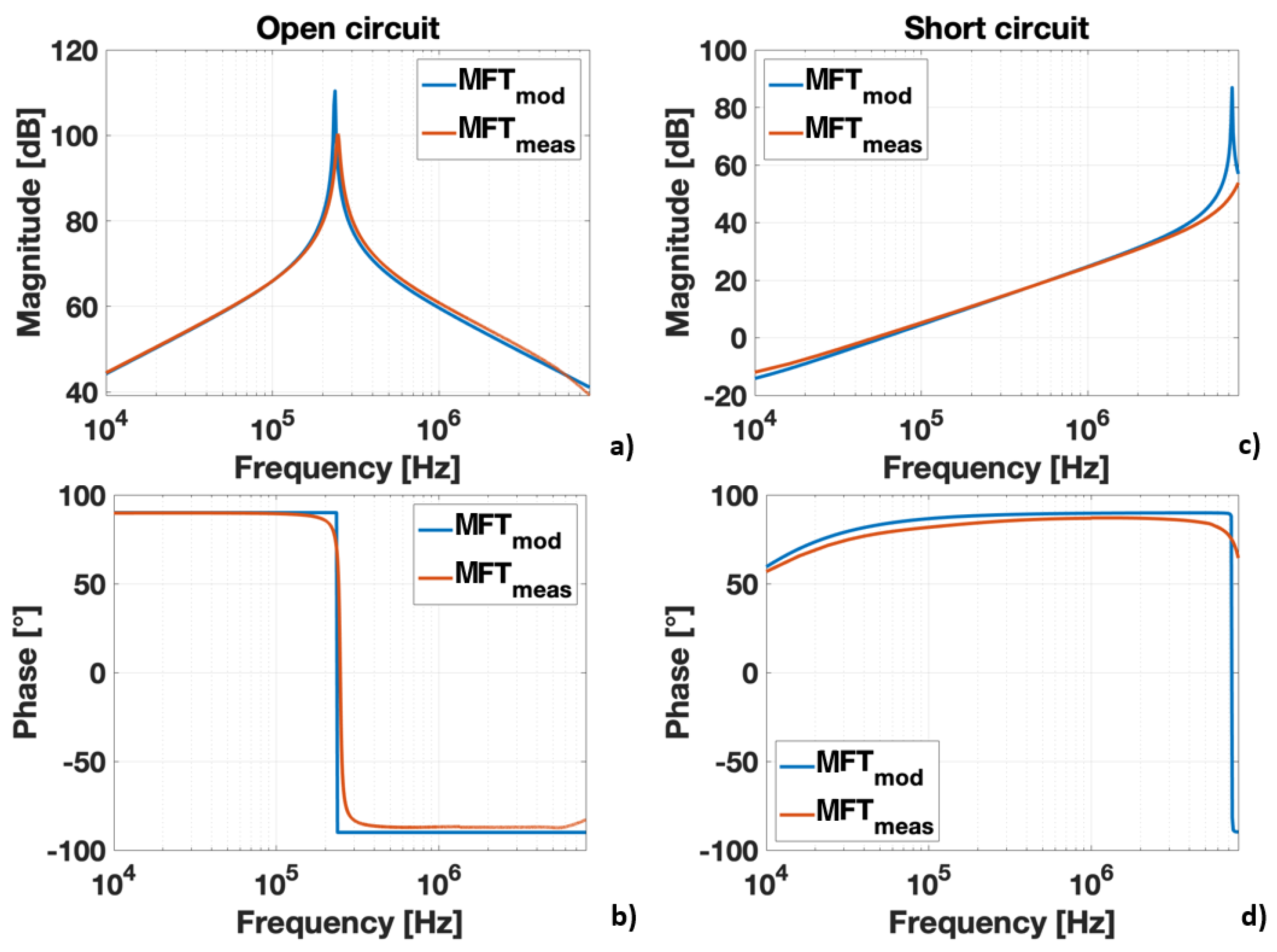
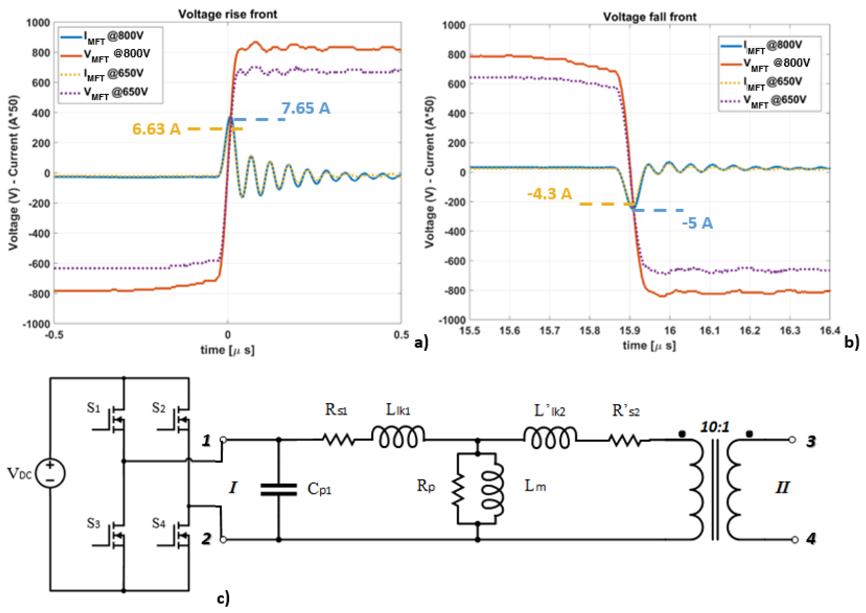
Figure 4 shows the comparison between the model obtained this way and the experimental measurements. From the results in Figure 4, it is possible to notice that the resonance frequency of the model and the measured one are 240 kHz and 243 kHz , respectively. Therefore, the error is 1.3 % confirming the precision of the adopted model. Another test was made to verify the value of the parasitic capacitance of the model. The test consists in feeding the DUT with a square wave to the voltage at open circuit conditions. To do this, an H-bridge converter was used, consisting of a WBG power module having SOA of 1200 V and 100 A . By measuring the magnetizing current of the DUT, it is possible to notice the current holes due to the capacitive affects. Two tests at 650 V and 800 V have been performed, voltage and current waveform are shown in Figure 5. The parameters of the model in Figure 6b were measured on a set of 10 planar HFTs. Table 1 shows the average values. The dispersion of the parameter is less than 1 % for the inductive parameters. This means that the transformers can be considered equal to each other.

3. Medium Frequency Transformers Models

A valid MFT model for application with a switching frequency between some kHz and some hundreds of kHz must include the inductive and capacitive parasitic elements. Those frequency response models can be addressed through their transfer functions [25]. The most adopted models in this frequency range are reported in Figure 1.
Parameters L lk 2 , L lk 1 in Figure 1 are the leakage inductance at the primary and secondary side, respectively. Those parameters are affected by winding interleaving, copper, and insulator thickness. L m is the magnetizing inductance, it depends on the material and geometry of the core.
The equivalent parasitic capacitance value depends on core and windings geometry. All parameters of the three models can be calculated analytically [26,28,29] or through experimental measurements, [27,30,32], thanks to the adoption of an LCR, experimental measurements can be performed [31]. Two MFT configurations are usually considered: open circuit (Figure 2a) and short circuit measurement (Figure 2b). The connection in Figure 2c is performed to measure the parasitic capacitance between primary and secondary windings.
Another experimental method for the parasitic capacitance evaluation in an MFT is to supply the Device Under Test (DUT) adopting a DC/AC converter [33]. Applying a square wave voltage to the MFT in open circuit conditions, the magnetized current passes through the primary winding Figure 5. The magnetizing current ideally has a triangular waveform but holes in the peaks of the triangular waveform appear. Those holes are due to the effects of parasitic capacitance excited by the high dV/dt values during commutations (Figure 3). Analytically, the voltage applied to the stray capacitance can be defined as in (9).
V Ceq = 1 C eq i Ceq d t
The amount of charge displaced in the equivalent parasitic capacitance is equal to the integral of the current in the switching time (10).
Q Ceq = i Ceq d t
The integral in (10) is the triangle area having the commutation time and current peak as the basis and the height, respectively (see Figure 3b). By substituting (10) in (9), the equivalent capacitance (11) can be evaluated.
C eq = I Ceq ( t 2 t 1 ) 4 V 1
The proposed IPOS modelization in this work adopts the model in (Figure 1a) like single MFT model. To verify the effectiveness of the single MFT model, a series of experimental tests have been performed.
The first series of experimental tests aims to validate the chosen model of MFT (Figure 1a). The DUT is a 20 kW planar transformer with a transformation ratio t equal to 10:1 (primary to secondary side). Looking at its data-sheet, the working frequency of the DUT can vary between 40 kHz and 1 MHz . Transformer parameters are estimated through measurements made with an LCR meter (Hioki-IM3536). The measuring terminals have compensation to carry out frequency measurements up to 8 MHz . The connections made during the parameters identification procedure are reported in Figure 2.
Figure 4 shows the comparison between the model obtained this way and the experimental measurements. From the results in Figure 4c, it is possible to notice that the magnitude of the model differs from the measured value of 0.7 dB resulting in a 7.8 % error. From Figure 4a the resonance frequency of the model and the measured one are 240 kHz and 243 kHz , respectively, therefore, the 1.3 % error is confirming the precision of the adopted model.
A further test is performed to verify the value of the parasitic capacitance of the model. The test consists of feeding the DUT with a voltage square wave to the nominal voltage at open circuit conditions (Figure 5c). By analyzing the DUT magnetizing current, it is possible to notice the currents holes due to the capacitive effects and then estimate it through (11). An H-bridge converter, consisting of a WBG power module having SOA of 1200 V and 100 A , was used. Two tests at 650 V and 800 V have been executed, voltage and current waveforms are reported in Figure 5.
The model parameters in Figure 6b were measured on a set of 10 planar MFTs. Table 1 shows the average values from the measurement over 10 DUTs. The dispersion of the parameter is less than 1 % for the inductive parameters. Hence, the transformers can be considered equal to each other.

4. Multi-Transformer Structure

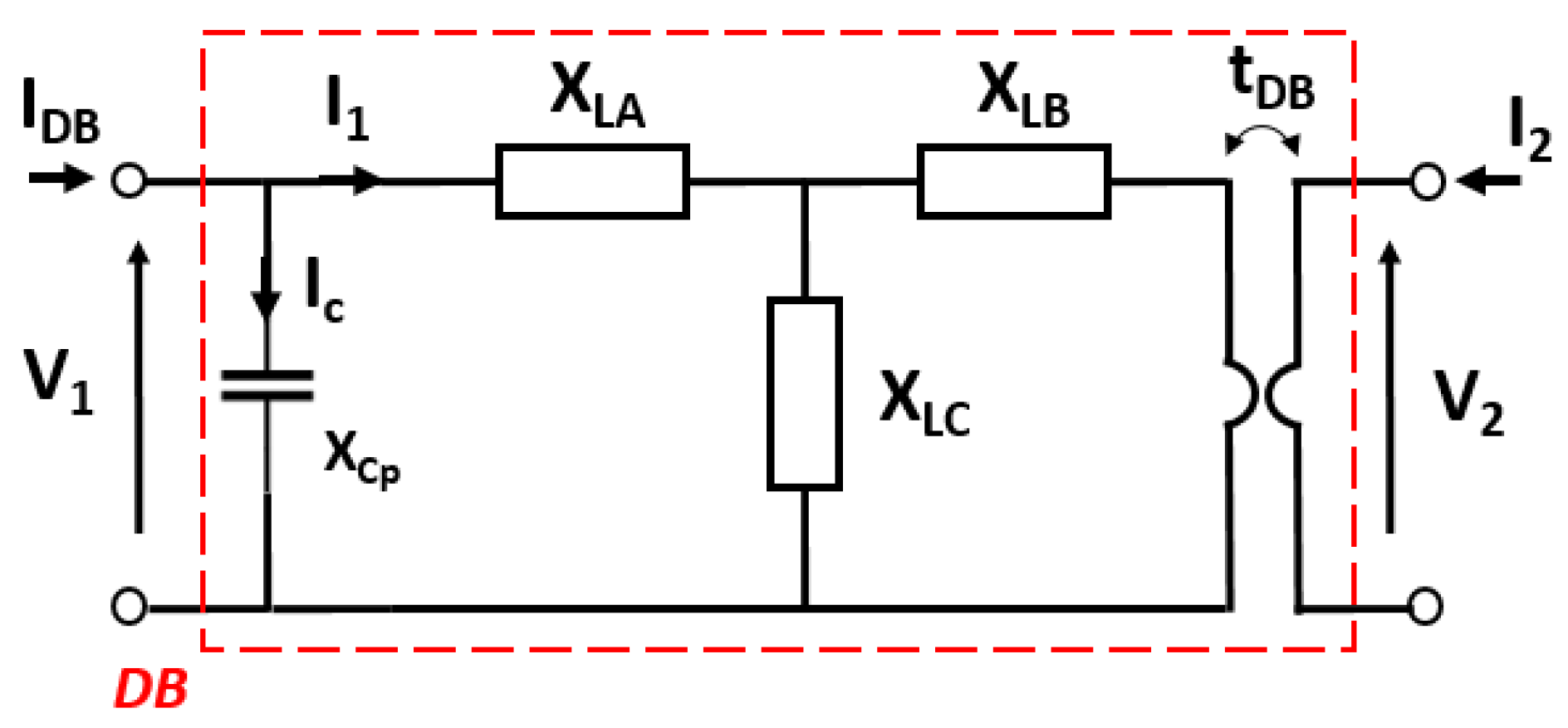
This section aims to derive a valid model of a multi-transformer structure according to the DB in Figure 6. The MFT model defined in Section 3 (Figure 1a) is a double bipole (DB) as shown in Figure 6. The model of a DB can generally be derived from the following equations:
[ V ] = [ Z ] · [ I ]
[ I ] = [ Y ] · [ V ]
where [Z] is the impedance matrix, [Y] admittance matrix, [V] and [I] are the voltage and current vectors of the primary and secondary sides. Furthermore, for the DB, hybrid matrices define the following relationships between specific voltages and currents.
V 1 I 2 = [ H ] · I 1 V 2
I 1 V 2 = [ H ] 1 · V 1 I 2
where V 1 and V 2 are the voltage at the primary and secondary side, respectively. I 1 and I 2 are the current at the primary and secondary side. [H] is the hybrid matrix and [ H ] 1 its inverse.
Connections between two or more DBs are summarized as follow:
  • Input Parallel Output Series (IPOS);
  • Input Series Output Parallel (ISOP);
  • Input Series Output Series (ISOS);
  • Input Parallel Output Parallel (IPOP).
Those connections can, in some cases, change the transformation ratio and the system rated power. Each of the above-listed connections defines a new multi-transformer structure. The new structure can be described through homogeneous ([Z], [Y]), or hybrid ([H], [ H ] 1 ) matrices. Depending on the connection the choice of the matrix which defines the single MFT, simplifies the calculation of the multi-transformer model. The final equivalent matrix will be a combination of the single MFT’s matrices. For the series connection, the matrix to be chosen is [Z] and for the parallel connection it is [Y]. In both cases, the equivalent matrix is given by the sum of all single matrices.
For the IPOS structure, the best matrix to be chosen is [ H ] 1 . Figure 6 defines a generic MFT two-port bipole in which the parasitic capacitance is included. Inductive parameters are connected in T configuration. In the DB, the equivalent transformer ratio t DB changes as a function of the multi-transformer connection.

4.1. Inductive Parameters

The first parameters calculation is related to the T connection of the inductive reactance referred to the equivalent DB circuit (Figure 6). This calculation adopts the [ H ] 1 matrix.
[ H ] 1 = h 11 h 12 h 21 h 22
The elements of the matrix [ H ] 1 are defined as follows:
h 11 i 1 v 1 a t ( i 2 = 0 ) ; h 12 i 1 i 2 a t ( v 1 = 0 ) ; h 21 v 2 v 1 a t ( i 2 = 0 ) ; h 22 v 2 i 2 a t ( v 1 = 0 ) ;
where h 11 represents the input admittance at no load conditions, h 12 is the current gain in short circuit conditions at the primary side, h 21 is the voltage gain at open circuit conditions, h 22 is the output impedance at short circuit conditions at the primary side. The inductive lumped-parameters of the individual MFT are defined through the Equation (18). X lk 1 is the inductive reactance related to the leakage inductance L lk 1 of the model in Figure 1a.
X LA = X lk 1 ; X LB = t 2 X lk 2 ; X LC = X m
Starting from the parameters defined in (18), the inverse hybrid matrix of the single MFT is defined in (19), where t is the transformation ratio of the single MFT.
[ H ] 1 = 1 X lk 1 + X m X m t ( X lk 1 + X m ) X m t ( X lk 1 + X m ) X lk 1 X lk 2 + X lk 2 X m + X lk 1 X m t 2 X lk 1 + X m
The electrical connection of an IPOS-N is schematically reported in Figure 7. The description of the single MFT through the inverse matrix allows to define an inverse matrix of the IPOS structure as:
[ H ] Tr eq 1 = [ H ] Tr 1 1 + [ H ] Tr 2 1 + + [ H ] TrN 1
where [ H ] TrN 1 is the hybrid matrix of the single MFT and the [ H ] Tr eq 1 is the hybrid matrix of the IPOS-N structure.
Making connections between multiple transformers, these must have the same parameters in order to avoid unbalances. The adoption of planar transformers satisfies this requirement (see Table 2), then the hypothesis to consider the matrix [ H ] TrN 1 identical for all connected transformer is valid. The equivalent hybrid matrix is:
[ H ] Tr eq 1 = N [ H ] Tr 1 1
where N is the number of connected transformers into the IPOS structure. Once the inverse matrix of the multi-transformer structure [ H ] Tr eq 1 has been calculated, it is necessary to make the conversion to obtain an equivalent impedance matrix [ Z ] eq .
The relation between the two matrices is defined in (22).
[ Z ] Tr eq = 1 h 11 Tr eq h 12 Tr eq h 11 Tr eq h 21 Tr eq h 11 Tr eq Δ [ H ] Tr eq 1 h 11 Tr eq
Starting from the inverse hybrid matrix [ H ] Tr eq 1 , making the required substitution in (22), the elements of [ Z ] eq can be calculated. The equivalent impedance matrix of an IPOS-N structure results in (23).
[ Z ] Tr eq = X lk 1 + X m N X m t X m t t 2 N X lk 2 + N X m t 2
On the other side, the impedance matrix [ Z ] eq can be defined through the element of the inductive T-model as shown in (24).
[ Z ] DB = X LA + X LC X LC t DB X LC t DB X LB t DB 2 + X LC t DB 2
From the element-by-element comparison of the two matrices in (24) and (23), a system with 4 variables and 3 equation is obtained. It is necessary to add the fourth equation, this is defined by the equivalent transformation ratio. In IPOS and ISOP connections, the transformation ratio differs from the single MFT one. To verify the input–output voltage ratio of an IPOS-N structure, Kirchhoff’s Voltage Law can be applied to the secondary side (Figure 7).
V DB = V 1 + V 2 + + V i + + V N
where V DB is the equivalent double bipole output voltage, V i is the secondary side voltage of the i-MFT. Using the single MFT ratio t, the secondary voltage can be expressed at the primary side as in (26).
V DB = V 1 t 1 + V 2 t 2 + + V i t i + + V N t N
Under the hypothesis that all MFTs have the same parameters, the equivalent voltage ratio is (27).
V DB = N V 1 t = > t DB = V 1 V DB = t N
The transformation ratio of an IPOS-N structure t DB is equal to the single MFT transformation ratio divided by the number of those connected to the structure.
From the comparison between (23) and (24), the elements X LA , X LB , and X LC of the IPOS model (Figure 6) can be calculated.
X LA = X lk 1 N
X LB = X lk 2 N
X LC = X m N ;
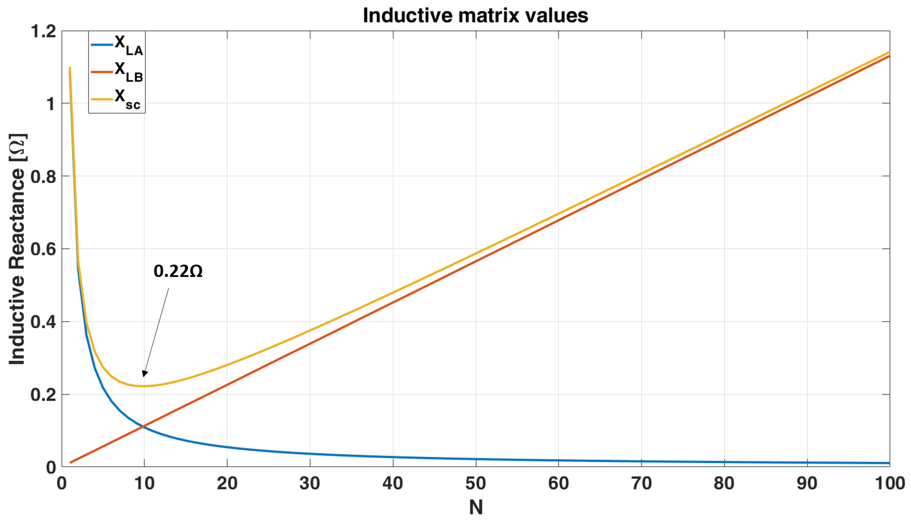
The primary side inductive reactance X LA , defined in (28), represents the parallel of all the MFTs connected in the structure. Thus, the inverse is proportional with the number of connected MFTs.
The inductive reactance at the secondary side X LB in (29) represents the series of all the inductive reactances of the individual MFTs. X LB is indeed proportional to the number of connected MFTs. As can be noticed in (30), X LC is proportional to the magnetization reactance and is divided by the number of connected transformers to the IPOS-N structure.
Substituting the parameters of the single MFT in Table 1 to Equations (28) and (29), the reactance values in the function of N are plotted in Figure 8. It can be noticed that, for N that tends to infinity, X LA tends to zero whereas X LB diverges. For N = t , both parameters achieve the same value.
The sum of the series parameters X LA and X LB defines the short circuit reactance X sc .
X sc = X LA + X LB = X lk 1 N + X lk 2 N
where X LA and X LB do not depend on the transformer ratio but only on the number of connected MTFs. From Figure 8, it can be seen that (31) presents the minimum point for N = 10 . Changing the transformer ratio, the minimum point does not change. The minimum value of the series parameter means minimum copper losses into the multi-transformer structure. Designing the IPOS structure for N = 10 leads to maximize the efficiency of the transformer stack.

4.2. Capacitive Parameters

With reference to the model in Figure 1a, the parasitic capacitance can be divided into two identical capacities ( C p / 2 ) . Those two capacities are connected to the primary and secondary sides of the equivalent DB (see Figure 9a). In an IPOS configuration, the seen equivalent capacitance from the primary side is the sum of two contributions (32). The first is defined by the parallel of the capacities connected to the primary side. The second will be given by the series of parasitic capacities to the secondary of the single MFTs.
C p 1 = N C p 2 ; C p 2 = C p 2 N t DB 2
where C p 1 is the capacitance at the parallel side connected and C p 2 is the capacitance, seen from the primary side, at the series-connected side. The equivalent parasitic capacitance of an IPOS-N structure can be calculated as indicated in (33).
C p DB = C p 2 N 2 t 2 + 1 N t 2
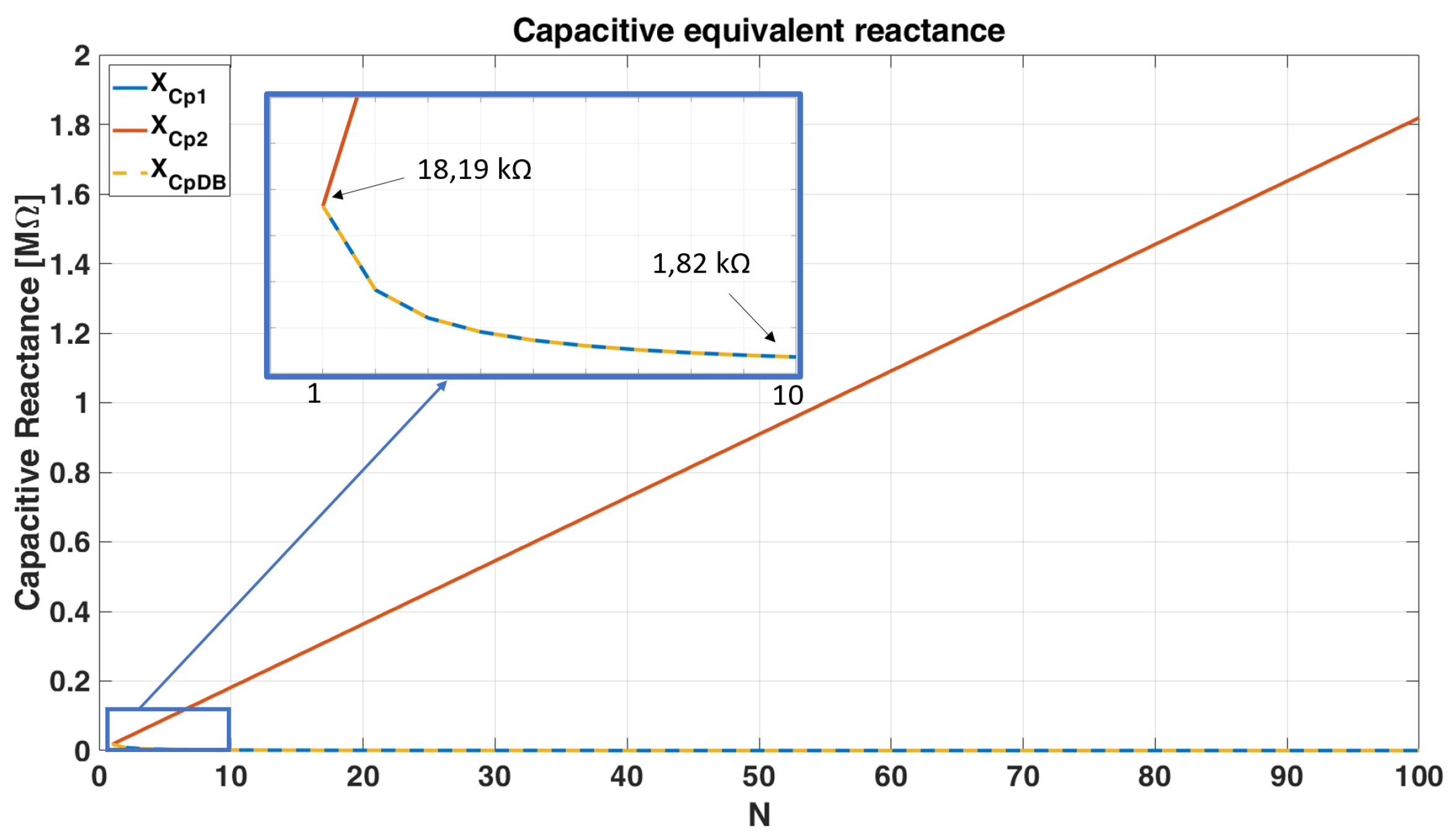
The reactive capacitance X CpDB related to C p DB can be expressed in the function of the connected MFTs to the structure Figure 10.
The equivalent capacitive reactance decrease and tend asymptotically to zero. Adopting the parameter of the single MFT in Table 1, for N = t the equivalent reactance is 1.82 k Ω . This value is some orders higher compared with the series parameters values, hence it can be neglected at the nominal condition.

4.3. Model Results

Combining the results from the previous subsections, a global impedance matrix is defined. The matrix in (34) describes an equivalent DB made by N-MFTs connected in IPOS configuration.
V 1 V 2 = Z 11 Z 12 Z 21 Z 22 · I DB I 2
where the matrix elements are defined as follows:
Z 11 = ( X LA + X LC ) X CpDB X LA + X LC + X CpDB
Z 12 = Z 21 = X LC X CpDB ( X LA + X LC + X CpDB ) t DB
Z 22 = ( X LA + X CpDB ) X LC ( X LA + X LC + X CpDB ) t DB 2 + X LB
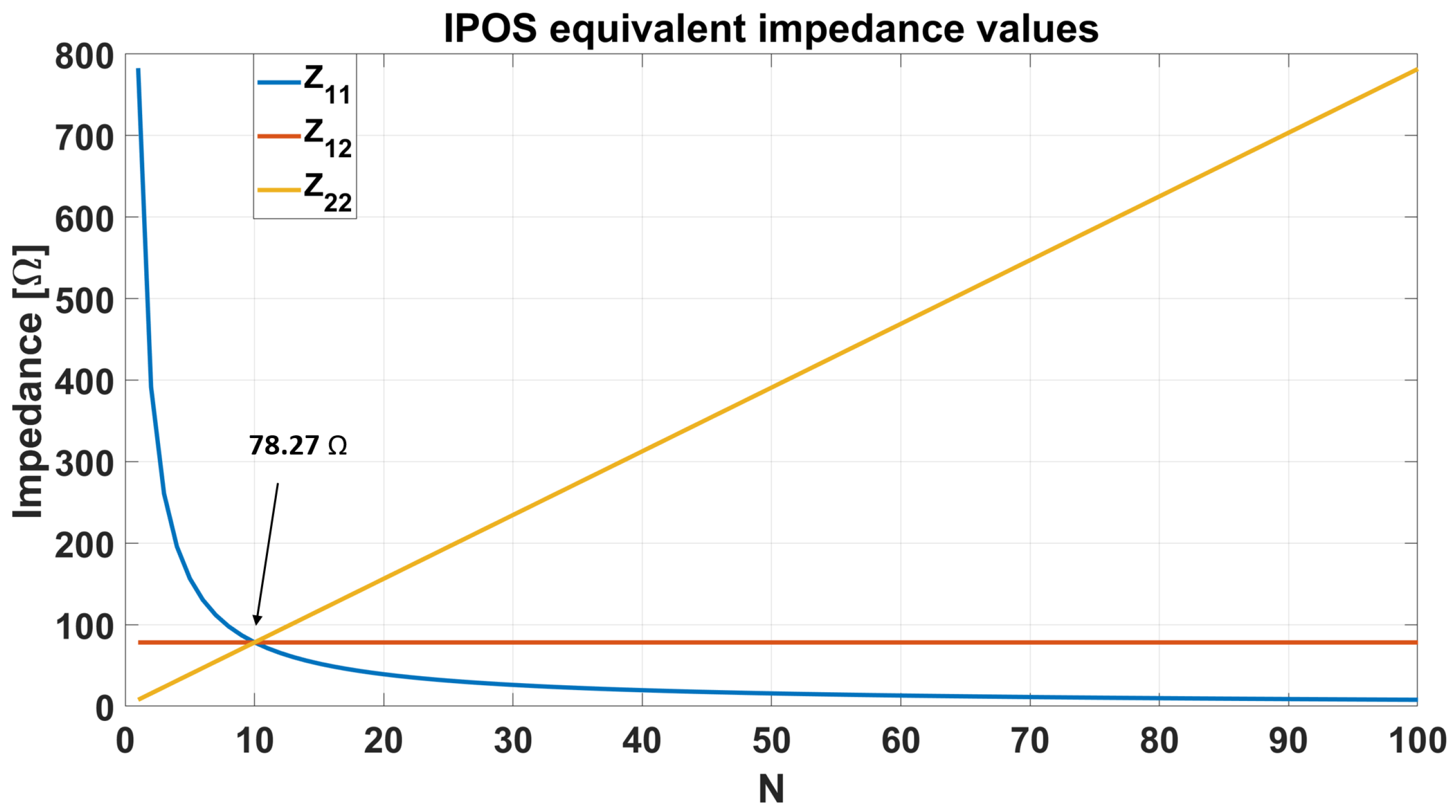
Substituting the value of the single MFT in Table 1, the matrix elements in the function of N are plotted in Figure 11. The important result of this modelization is provided for N = t . In this case, all matrix elements defined in Equations (35)–(37) assume the same value (38). This consideration is valid for transformers in which L sc < < L m ; thus, the value in (38) depends on the parasitic capacitance and the magnetize inductance.
Z 11 = Z 12 = Z 21 = Z 22 = Z = 2 L m t 2 C pDB 2 π f L m t + 1 π f t C pDB
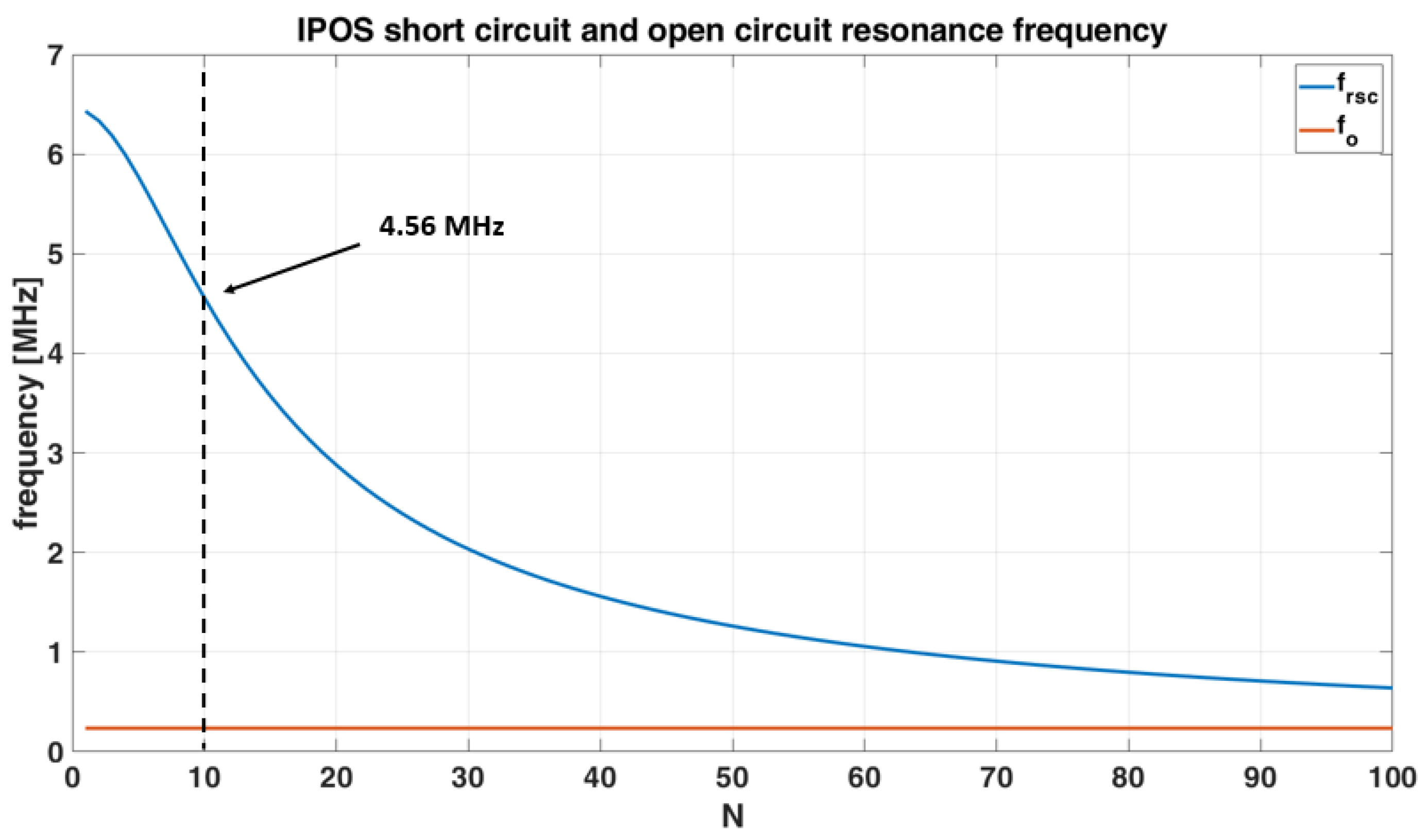
Another consideration should be made about the resonance frequency. The open circuit f 0 , IPOS and short circuit f sc , IPOS resonance frequencies are defined in (39) and (40), respectively.
f 0 , IPOS = 1 2 π L in C pDB
f sc , IPOS = 1 2 π L sc C pDB
where L in is input inductance measured by the LCR meter and listed in Table 3. The L sc is the short circuit inductance composed by the sum of the L A and L B terms. Figure 12 shows the resonance frequencies in the function of N. The open-circuit resonance does not change increasing N, whereas the short circuit resonance frequency decreases while N increases. This result suggests the designer a way to select N still to meet the frequency response requirements. Choosing higher N values leads to lowering the resonance frequency of the system resulting in an introduction of the currents and voltage ringing into the system.

5. Experimental Validation

This section aims to present the experimental result concerning the model validation, then the IPOS-10 as an application for 200 kW is presented. The same tests described in Section 3 have been performed on the IPOS-N structure. Validation for IPOS-N structures with a different number of transformers has been executed, in particular: IPOS-2, IPOS-5, IPOS-6, and IPOS-10.

5.1. IPOS-N Model Validation

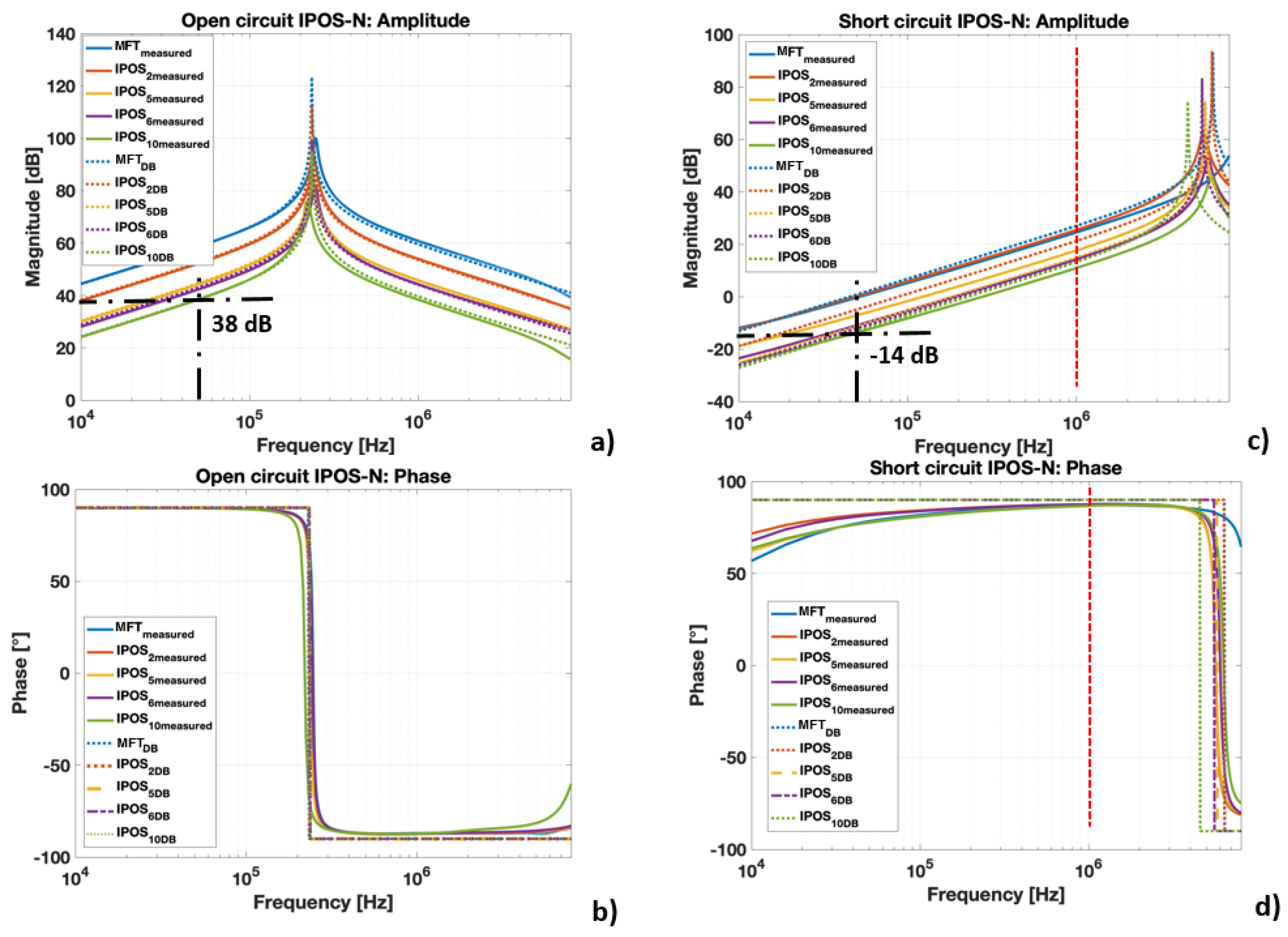
In Figure 13, the measurements and the respective frequency responses of the previously mentioned IPOS-N structures are reported. In addition, in this case, the model correctly follows the frequency behavior obtained through the experimental tests.
An aspect to underline is the unchanged resonance frequency of the system in all the proposed IPOS-N solutions. Resonant frequency does not change with the increase in the number of MFTs connected to the structure. This result allows building a 200 kW transformer maintaining the single MFT frequency limitations.
From Figure 13a, analytical models maintain the same resonance frequency, whereas the measurements deviate by a maximum of 10 kHz resulting in a 4 % error. The impedance magnitude for the IPOS-10 is 38 dB (79.4 k Ω ) at 50 kHz resulting in a 2 % error compared to the measurements. This error is mainly due to the connections between the various MFTs in the IPOS-N structure. Increasing the number of MFTs, electrical connections affect the resonant frequency lowering it. Connection parasitisms are not taken into account in the model.
At nominal condition, the frequency working range for the single MFT is from 40 kHz to 1 MHz following the indications of the manufacturer. The experimental tests carried out that in short circuit conditions the resonance frequency for these transformers is around 6 MHz (see Figure 13c). Equation (31) can be used to compare the measured value with the obtained model one. For the IPOS-10 configuration, the calculated short circuit reactance (31) is equal to 222 m Ω . In short circuit conditions, the measurement at 50 kHz is equal to 199 m Ω (−14dB) resulting in a 10 % error.
The comparison between the experimental results and the obtained model, in Figure 13c, shows that the inductive behavior under nominal conditions is guaranteed. The resonance frequencies remain far from the frequency working range.
All the values adopted in the models and those obtained experimentally are listed in Table 3. LCR-meter experimental set-ups are shown in Figure 14g.

5.2. IPOS-10 Power Test

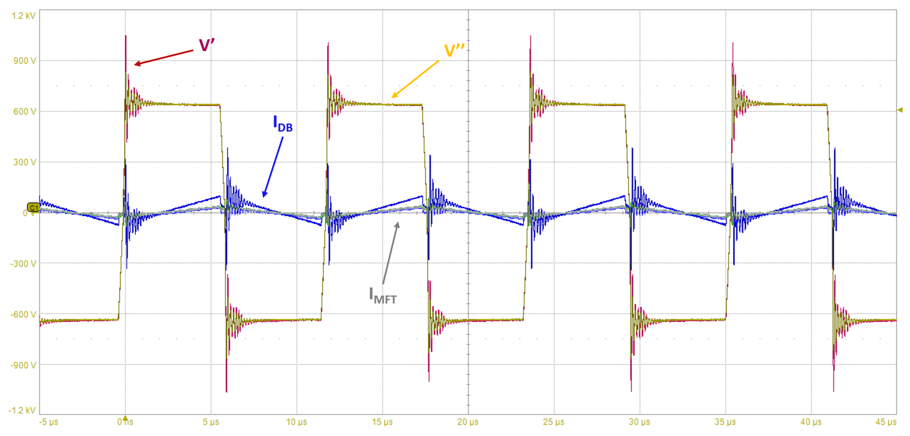
To verify the equally shared current between the connected MFTs to the IPOS-10, two tests have been performed. The first test at open circuit connection in Figure 15 shows that the magnetized current I DB is equally distributed among all MFTs, indeed the current in a single MFT is equal to 0.75 A , resulting in a global magnetized current of 7.5 A . The open circuit test bench for IPOS-10 is shown in Figure 14a,f.
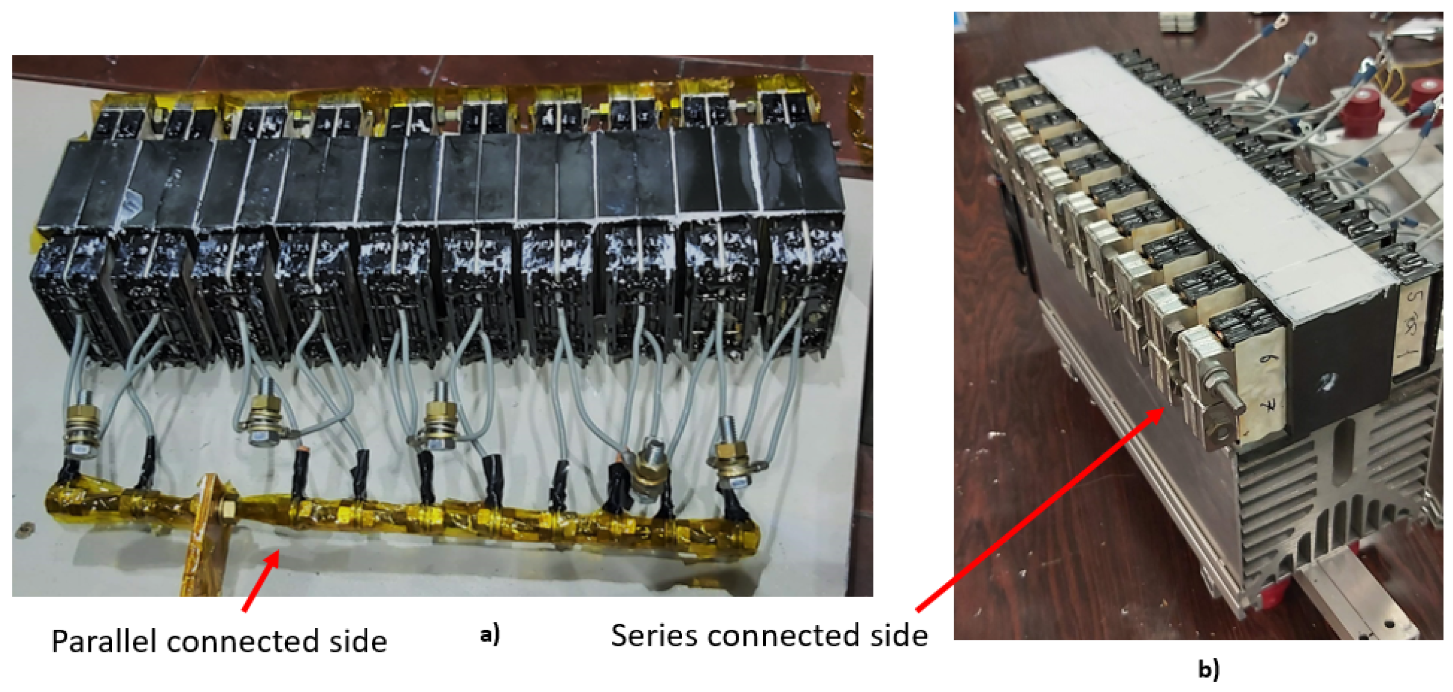
The second test is performed at nominal conditions in an 800 V application. For the 200 kW SST three-phase converter, three IPOS-10s have been adopted in star connection. Figure 16 presents the results, underling the equally distribution of the current among the MFTs connected to one IPOS-10. Figure 17 shows the final IPOS-10 structure adopted for the power tests.

6. Conclusions

The paper proposes an IPOS-10 as an innovative multi-MFT structure for SST converters implying the use of 10 10:1 transformers leading to a 1:1 final equivalent transformer. This solution allows adjusting the voltage ratio by connecting different transformers to the IPOS structure. Moreover, it increases the power density of the converter. The frequency behavior does not change passing from the single MFT to the IPOS-N configuration, both in open circuit and in short circuit conditions.
The adoption of an IPOS structure with the number of connected transformers equal to the transformer ratio minimize the short circuit impedance. Furthermore, the matrix that describes the IPOS structure for N = t becomes a matrix in which all elements assume the same value. Starting from the single MFT model, it is possible to calculate the equivalent model of the IPOS-N structure. Experimental tests show the validity of the adopted model.
The power tests demonstrate that the IPOS-10 structure can be adopted for single and three-phase SST converters as long as the current is equally shared among all MFTs resulting in a balanced system.
The adoption of a multi-transformer structure provides the designer with a further degree of freedom in modulating the system power rate.

Author Contributions

All the authors gave their contribution to all of the aspects of the manuscript. All authors have read and agreed to the published version of the manuscript.

Funding

This research received no external funding.

Conflicts of Interest

The authors declare no conflict of interest.

References

  1. Ruffo, R.; Guglielmi, P.; Armando, E. Inverter Side RL Filter Precise Design for Motor Overvoltage Mitigation in SiC-Based Drives. IEEE Trans. Ind. Electron. 2020, 67, 863–873. [Google Scholar] [CrossRef]
  2. La Ganga, A.; Guglielmi, P.; Armando, E. Auxiliary circuit design for soft switching in medium voltage application using 1.7 kV SiC MOSFET. In Proceedings of the 2018 IEEE International Telecommunications Energy Conference (INTELEC), Turino, Italy, 7–11 October 2018; pp. 1–5. [Google Scholar]
  3. Kumar, V.; Satpathy, S.; Lakshminarasamma, N. Analysis and design methodology for Planar Transformer with low self-capacitance used in high voltage flyback charging circuit. In Proceedings of the 2016 IEEE International Conference on Power Electronics, Drives and Energy Systems (PEDES), Trivandrum, India, 14–17 December 2016; pp. 1–5. [Google Scholar]
  4. Shafaei, R.; Saket, M.A.; Ordonez, M. Thermal Comparison of Planar Versus Conventional Transformers Used in LLC Resonant Converters. In Proceedings of the 2018 IEEE Energy Conversion Congress and Exposition (ECCE), Portland, OR, USA, 23–27 September 2018; pp. 5081–5086. [Google Scholar]
  5. Carsten, B.W. The low leakage inductance of planar transformers; fact or myth? In Proceedings of the (APEC 2001) Sixteenth Annual IEEE Applied Power Electronics Conference and Exposition (Cat. No.01CH37181), Anaheim, CA, USA, 4–8 March 2001; Volume 2, pp. 1184–1188. [Google Scholar]
  6. Taha, M.A.; Oumar, D.A.; Abderahim, A.; Capraro, S.; Pietroy, D.; Chatelon, J.P.; Rousseau, J.J. Simulation, Modeling, Manufacturing, and Characterization of a Planar Magnetic Face to Face Integrated Transformer. IEEE Trans. Magn. 2018, 54, 1–6. [Google Scholar] [CrossRef]
  7. Ouyang, Z.; Thomsen, O.C.; Andersen, M.A.E. The analysis and comparison of leakage inductance in different winding arrangements for planar transformer. In Proceedings of the 2009 International Conference on Power Electronics and Drive Systems (PEDS), Taipei, Taiwan, 2–5 November 2009; pp. 1143–1148. [Google Scholar]
  8. Tria, L.A.R.; Zhang, D.; Fletcher, J.E. High-Frequency Planar Transformer Parameter Estimation. IEEE Trans. Magn. 2015, 51, 1–4. [Google Scholar] [CrossRef]
  9. Candolfi, S.; Viarouge, P.; Aguglia, D.; Cros, J. FEA identification of high order generalized equivalent circuits for MF high voltage transformers. In Proceedings of the 17th European Conference on Power Electronics and Applications, Geneva, Switzerland, 8–10 September 2015. [Google Scholar]
  10. Zhu, J.G.; Hui, S.Y.R.; Ramsden, V.S. A generalized dynamic circuit model of magnetic cores for low and high frequency applications. I. Theoretical calculation of the equivalent core loss resistance. IEEE Trans. Power Electron. 1996, 11, 246–250. [Google Scholar] [CrossRef]
  11. Hui, S.Y.R.; Zhu, J.G.; Ramsden, V.S. A generalized dynamic circuit model of magnetic cores for low- and high-frequency applications. II. Circuit model formulation and implementation. IEEE Trans. Power Electron. 1996, 11, 251–259. [Google Scholar] [CrossRef]
  12. Chen, M.; Araghchini, M.; Afridi, K.K.; Lang, J.H.; Sullivan, C.R.; Perreault, D.J. A Systematic Approach to Modeling Impedances and Current Distribution in Planar Magnetics. IEEE Trans. Power Electron. 2016, 31, 560–580. [Google Scholar] [CrossRef]
  13. Arturi, C.M.; Gandelli, A. High frequency models of PCB-based transformers. In Proceedings of the 44th IEEE Midwest Symposium on Circuits and Systems, Dayton, OH, USA, 14–17 August 2001. [Google Scholar]
  14. Habibinia, D.; Feyzi, M.R. Optimal winding design of a pulse transformer considering parasitic capacitance effect to reach best rise time and overshoot. IEEE Trans. Dielectr. Electr. Insul. 2014, 21, 1350–1359. [Google Scholar] [CrossRef]
  15. Vijaya Kumar, N.; Lakshminarasamma, N. Comparison of Planar Transformer Architectures and Estimation of Parasitics for High Voltage Low Power DC-DC Converter. In Proceedings of the 2018 IEEE International Conference on Power Electronics, Drives and Energy Systems (PEDES), Chennai, India, 18–21 December 2018; pp. 1–6. [Google Scholar]
  16. Kong, P.; Lee, F.C. Transformer structure and its effects on common mode EMI noise in isolated power converters. In Proceedings of the 2010 Twenty-Fifth Annual IEEE Applied Power Electronics Conference and Exposition (APEC), Palm Springs, CA, USA, 21–25 February 2010; pp. 1424–1429. [Google Scholar]
  17. Lu, J.; Dawson, F. Characterizations of High Frequency Planar Transformer with a Novel Comb-Shaped Shield. IEEE Trans. Magn. 2011, 47, 4493–4496. [Google Scholar] [CrossRef]
  18. Cochrane, D.; Chen, D.Y.; Boroyevic, D. Passive cancellation of common-mode noise in power electronic circuits. IEEE Trans. Power Electron. 2003, 18, 756–763. [Google Scholar] [CrossRef]
  19. Chen, R.; van Wyk, J.D.; Wang, S.; Odendaal, W.G. Improving the Characteristics of integrated EMI filters by embedded conductive Layers. IEEE Trans. Power Electron. 2005, 20, 611–619. [Google Scholar] [CrossRef]
  20. Tan, W.; Margueron, X.; Duquesne, T.; Idir, N. An Improved Parasitic Capacitance Cancellation Method for Planar Differential Mode Inductor in EMI Filters. In Proceedings of the 2012 7th International Conference on Integrated Power Electronics Systems (CIPS), Nuremberg, Germany, 6–8 March 2012; pp. 1–6. [Google Scholar]
  21. Chan, Y.P.; Pong, B.M.H.; Poon, N.K.; Liu, J.C.P. Common-Mode Noise Cancellation by an Antiphase Winding in Multilayer Isolated Planar Transformer. IEEE Trans. Electromagn. Compat. 2014, 56, 67–73. [Google Scholar] [CrossRef]
  22. Chen, R.; van Wyk, J.D.; Wang, S.; Odendaal, W.G. Planar electromagnetic integration technologies for integrated EMI filters. In Proceedings of the 38th IAS Annual Meeting on Conference Record of the Industry Applications Conference, Salt Lake City, UT, USA, 12–16 October 2003; Volume 3, pp. 1582–1588. [Google Scholar]
  23. Ortiz, G.; Leibl, M.; Kolar, J.W.; Apeldoorn, O. Medium frequency transformers for solid-state-transformer applications—Design and experimental verification. In Proceedings of the 2013 IEEE 10th International Conference on Power Electronics and Drive Systems (PEDS), Kitakyushu, Japan, 22–25 April 2013; pp. 1285–1290. [Google Scholar] [CrossRef]
  24. Spánik, P.; Fé, I.L.; Kácsor, G. Using planar transformers in soft switching dc/dc power converters. Adv. Electr. Electron. Eng. 2011, 3, 59–65. [Google Scholar]
  25. Shafiei, N.; Pahlevaninezhad, M.; Farzanehfard, H.; Bakhshai, A.; Jain, P. Analysis of a Fifth-Order Resonant Converter for High-Voltage DC Power Supplies. IEEE Trans. Power Electron. 2013, 28, 85–100. [Google Scholar] [CrossRef]
  26. Ouyang, Z.; Hurley, W.G.; Andersen, M.A.E. Improved Analysis and Modeling of Leakage Inductance for Planar Transformers. IEEE J. Emerg. Sel. Top. Power Electron. 2019, 7, 2225–2231. [Google Scholar] [CrossRef] [Green Version]
  27. Lu, H.Y.; Zhu, J.G.; Hui, S.R. Experimental determination of stray capacitances in high frequency transformers. IEEE Trans. Power Electron. 2003, 18, 1105–1112. [Google Scholar] [CrossRef] [Green Version]
  28. Ackermann, B.; Lewalter, A.; Waffenschmidt, E. Analytical modelling of winding capacitances and dielectric losses for planar transformers. In Proceedings of the 2004 IEEE Workshop on Computers in Power Electronics, Urbana, IL, USA, 15–18 August 2004. [Google Scholar]
  29. Biela, J.; Kolar, J.W. Using Transformer Parasitics for Resonant Converters—A Review of the Calculation of the Stray Capacitance of Transformers. IEEE Trans. Ind. Appl. 2008, 44, 223–233. [Google Scholar] [CrossRef]
  30. Lu, H.Y.; Zhu, J.G.; Ramsden, V.S.; Hui, S.Y.R. Measurement and modeling of stray capacitances in high frequency transformers. In Proceedings of the 30th Annual IEEE Power Electronics Specialists Conference, Charleston, SC, USA, 1 July 1999. [Google Scholar]
  31. Lu, H.Y.; Zhu, J.G.; Ramsden, V.S. Comparison of experimental techniques for determination of stray capacitances in high frequency transformers. In Proceedings of the IEEE 31st Annual Power Electronics Specialists Conference, Galway, Ireland, 23 June 2000. [Google Scholar]
  32. Baccigalupi, A.; Daponte, P.; Grimaldi, D. On a circuit theory approach to evaluate the stray capacitances of two coupled inductors. IEEE Trans. Instrum. Meas. 1994, 43, 774–776. [Google Scholar] [CrossRef]
  33. Ganga, A.L.; Reyhan, S.; Re, R.; Dalbavie, J.M.; Guglielmi, P. Losses and thermal considerations on an IPOS structure with 20kW high-frequency planar transformers. In Proceedings of the 2020 International Conference on Electrical Machines (ICEM), Gothenburg, Sweden, 23–26 August 2020; Volume 1, pp. 921–926. [Google Scholar] [CrossRef]
Figure 1. Model of a Medium-Frequency transformer adopting six (c), three (b), and one (a) equivalent capacitance, respectively.
Energies 14 01450 g001
Figure 2. Measurement connections to identify the equivalent model parameters. Open circuit (a), short circuit (b), and primary to secondary (c) connections.
Energies 14 01450 g002
Figure 3. Ideal voltage (red) and current (blue) applied to the primary of the HFT (a). Equivalent current due to the parasitic capacitive effects (b).
Energies 14 01450 g003
Figure 4. Frequency sweep comparison between the Medium Frequency Transformer (MFT) model and the measurement: module and phase in open circuit (a,b) in short circuit (c,d), respectively.
Energies 14 01450 g004
Figure 5. Voltage and current waveforms in an open circuit test at nominal voltage. Voltage rise front (a) and fall front (b) details. Probe scale 200 V / div and 5 A / div . Power test scheme at open circuit (c).
Energies 14 01450 g005
Figure 6. Definition of the MFT as double bipole in which the equivalent voltage ratio t DB depends on the multiple-transformer structure connections.
Energies 14 01450 g006
Figure 7. Equivalent electric circuit of an Input Parallel Output Series (IPOS)-N structure based on a connection between single capacitance models of a high frequency transformer.
Energies 14 01450 g007
Figure 8. Inductive reactance values in function of the number of connected transformers N to the IPOS structure. The reactance is calculated for the measured parameters listed in Table 1 at 50 kHz .
Energies 14 01450 g008
Figure 9. Equivalent electric model of the lumped capacitive reactance at the primary and secondary sides (a) of the double bipole (DB). Two contributions of the total capacitive reactance seen from the primary side (b).
Energies 14 01450 g009
Figure 10. Capacitive reactance values in the function of the number of connected transformers N to the IPOS structure. The reactance is calculated for the measured parameters listed in Table 1 at 50 kHz .
Energies 14 01450 g010
Figure 11. IPOS equivalent matrix values in the function of the number of connected transformers N. The reactance is calculated for the measured parameters listed in Table 1 at 50 kHz .
Energies 14 01450 g011
Figure 12. IPOS-N short circuit and open circuit resonance frequencies in the function of the connected MFT to the IPOS structure.
Energies 14 01450 g012
Figure 13. Magnitude (a) and phase (b) comparison between DB model and measurement results for different IPOS-N structures at open circuit conditions; magnitude (c) and phase (d) comparison between DB model and measurement results for different IPOS-N structures at short circuit conditions. The red dashed line in (c,d) defines the frequency operation limit of the single MFT.
Energies 14 01450 g013
Figure 14. (a) Experimental test bench; (b) MFT power set-up; (c) IPOS-2 power set-up; (d) IPOS-5 power set-up; (e) IPOS-6 power set-up; (f) IPOS-10 power set-up; (g) test bench for frequency sweep measurement: from 50 Hz to 8 MHz .
Energies 14 01450 g014
Figure 15. IPOS-10 structure for 200 kW Solid State Transformer (SST) converter: test in open circuit conditions. Primary ( V —magenta trace) and secondary ( V —yellow trace) side voltage scale 300 V/div, total IPOS-10 magnetized current ( I DB —blue trace) scale 20 A/div and single MFT magnetized current ( I MFT —gray trace) scale 5 A/div, time scale 5 μ s/div.
Energies 14 01450 g015
Figure 16. IPOS-10 structure for 200 kW SST converter: test in a three phase SST Dual Active Bridge. Phase-to-phase voltages ( V uv —blue trace) ( V vw —green trace) ( V wu —yellow trace) at the primary side scale 500 V/div, total IPOS-10 phase current ( I DB —red trace) scale 100 A/div, and single MFT magnetized current ( I MFT —gray trace) scale 100 A/div, time scale 5 μ s/div.
Energies 14 01450 g016
Figure 17. IPOS-10 structure for 200 kW SST converter. Details of the parallel connection at the primary side (a) and series connection at the secondary side (b).
Energies 14 01450 g017
Table 1. Average of the measured parameters over 10 single-phase 20 kW planar MFTs.
MFT ParametersSymbolValueStandard Deviation
Primary leakage inductance L lk 1 3.465 μ H 227.2 nH
Secondary leakage inductance L lk 2 35 nH 2.62 nH
Magnetize inductance L m 2.6 mH 0.241 mH
Parasitic capacitance C p 350 pF 32.5 pF
Table 2. Parameters of a single phase 20 kW high frequency planar transformer.
HFT ParametersSymbolValue
Primary leakage inductance L lk 1 3.465 μ H
Secondary leakage inductance L lk 2 35 nH
Magnetize inductance L m 2.6 mH
Parasitic capacitance C p 350 pF
Table 3. Values of the IPOS-N equivalent model.
IPOS-2 ParametersModelMeasuredError
L A 1 mH --
L B 26.3 μ H--
L C 260 μ H--
L in 1.26 mH 1.16 mH 8.6 %
C p 350.9 pF 313 pF 11 %
IPOS-5 ParametersModelMeasuredError
L A 260 μ H--
L B 105.3 μ H--
L C 260 μ H--
L in 520 μ H 532 μ H 2.3 %
C p 875.3 pF 968.4 pF 9.6 %
IPOS-6 ParametersModelMeasuredError
L A 173.3 μ H--
L B 131.6 μ H--
L C 260 μ H--
L in 433.3 μ H 412 μ H 5.2 %
C p 1.05 nF 950 pF 10.5 %
IPOS-10 ParametersModelMeasuredError
L A 34.65 nH --
L B 236.6 μ H--
L C 260 μ H--
L in 260 μ H 255 μ H 1.9 %
C p 1.75 nF 1.9 nF 8 %
Publisher’s Note: MDPI stays neutral with regard to jurisdictional claims in published maps and institutional affiliations.