Abstract
In this study, an adaptive driving method for synchronous rectification in bidirectional full-bridge LLC resonant converters used in railway applications is proposed. The drain to source voltage of the synchronous rectifier is utilized to detect the conduction of the body diode, and a suitable driving signal for synchronous rectification is generated accordingly. The proposed driving scheme is simple and can be realized using a low-cost digital signal processor (DSP). According to the experimental results, which averaged 0.4625% and 1.097%, improvement can be observed under charging and discharging mode, respectively.
1. Introduction
Owing to the continuous development and progress of society in recent years, the demand for electricity conversion has increased. However, the awareness of the limited earth resources has risen in recent years, awakening the consciousness of being environmentally friendly, as well as saving energy and reducing carbon dioxide emission, such as by trying to exert the energy most efficiently within the limited resources; a well-designed power system can be regarded as an essential way to save energy. Therefore, efficiency, lightness, thinness, shortness, and miniaturization have become important considerations in engineering design. Since the public’s requirements for power efficiency has never been higher, compared with linear power converters, switching power converters have an edge in high efficiency; furthermore, because power switches only work in the on and off states, it has less loss and heat. Therefore, the volume of the heat dissipator can be reduced. Moreover, the operating frequency of the switching power converter can be enhanced, thus reaching the requirement of being thinner and smaller, as well as having high-efficiency density.
Although DC-to-DC converters can minimize their volumes by enhancing the switching frequency, a higher switching loss [1] will be generated when conventional hard switching is used, leading to decreased efficiency and increased electromagnetic interference. In order to reduce the switching loss caused by hard switching, converter topologies possessing soft switching characteristics, such as zero voltage switching (ZVS) [2,3] and zero current switching (ZCS) [4], are commonly adopted. For converter topologies with soft switching characteristics, phase shifted full bridge (PSFB) and LLC resonant converters both have excellent characteristics [5]. PSFB has the strengths of fixed frequency operation, and using PSFB allows the circuit’s primary side to achieve ZVS to reduce the loss. However, in order to output a large current, a current doubler circuit is often utilized, but the current doubler circuit has too many magnetic elements, which are not in favor of enhancing power density. LLC resonant converters can achieve zero voltage switching (ZVS) with primary-/secondary-side switches, affording good performances in terms of efficiency [6,7,8]. In addition, LLC resonant converters can reduce the size of magnetic components by operating at high frequencies to achieve high power densities. Therefore, they are widely used as DC-DC converters for smart grid applications and railway power systems [9,10,11]. As an important mode of transportation on land, railways carry hundreds of millions of passengers annually. Therefore, the central control system on the train is extremely important because if the power system fails during a journey, the consequences will be disastrous. Hence, to ensure that normal operation is maintained during a power supply failure, trains are typically equipped with an additional emergency power supply device. Once the main system fails, the backup battery will provide temporary power supply to ensure the safety of the train and passengers. Hence, this paper focuses on the efficiency improvement of bidirectional full-bridge LLC resonant converters used in railway applications owing to its important role in providing an emergency power supply with high efficiency.
To improve the overall efficiency of bidirectional full-bridge LLC resonant converters, MOSFET are often used to replace power diodes on the secondary side. The following synchronous rectifier (SR) driving schemes have been proposed [12,13,14,15,16,17]: The first scheme senses and analyzes a current through a switch on the secondary side to generate an SR drive signal [12,13]. Although this method is highly accurate, sensing the secondary-side current requires a magnetic inductor; this increases not only the size, but also the resistance when connected in series, resulting in a low efficiency. The second method senses a current through the primary-side transformer, followed by driving signal generation after analysis [14,15]. This method requires additional magnetic inductors, causing additional resistive losses. Researchers have proposed generating the drive signal by sensing and analyzing the current on the resonant inductor; however, this increases the complexity of the sensing circuit owing to the need to sense the excitation current [16,17]. The authors of [18] proposed a method to sense the drain to source voltage on SR switch and adjust the gating signal of an SR switch adaptively. The complexity of this method is low, the circuit is simple to construct, and the firmware is relatively easy to implement. However, the methods above are suitable only for generating the SR signals of a unidirectional half-bridge LLC resonant converter, and not suitable for a bidirectional full-bridge LLC resonant converter, as their resonant tanks are only designed for a single direction. Regarding resonant tanks, Severns proposed multiple designs and analyzed various resonant tanks [19], whereas Lu et al. modified the resonant tanks proposed by Severns and proposed a resonant tank suitable for bidirectional DC-DC converters, while reducing the resonant components to merely four and accounting for the bidirectional power transmission [20]. Based on the adaptive SR driving technique proposed in [18], the design of a resonant tank is incorporated, and an adaptive SR driving strategy suitable for a bidirectional full-bridge LLC resonant converter is proposed in this study. As a result, the main contribution of this study is to propose an adaptive SR driving strategy applicable for bidirectional full-bridge LLC resonant converters. As shown in Figure 1, the timing to switch on/off in both directions can be determined through the current-sensing circuit of the switch. Moreover, the requirement for the functions to be realized by the microcontroller unit (MCU) can be reduced owing to the adaptive algorithm proposed herein and a four-channel controllable multiplex circuit, as they can be used even on low-cost MCUs. According to the experimental results, the adopted synchronous rectification driving strategy has a noticeable improvement in efficiency compared to the conventional SR driving method. The highest charging mode efficiency reaches 93.35%, and the most obvious difference between the conventional SR driving technique and the proposed method in the charging mode is 1%, enhancing by 0.462% on average. On the other hand, the discharging mode’s highest efficiency is 95.82%, and the most apparent difference between the conventional SR driving technique and the proposed approach in the discharging mode is 1.65%, enhancing by 1.097% on average. This paper is organized as follows: Section 2 proposes the theory and design approach of the resonant tank. In Section 3, this study proposes the adaptive SR driving strategy; in Section 4, the realization method of the adaptive SR driving is introduced; in Section 5, the experimental results are demonstrated. Lastly, Section 6 summarizes the study.
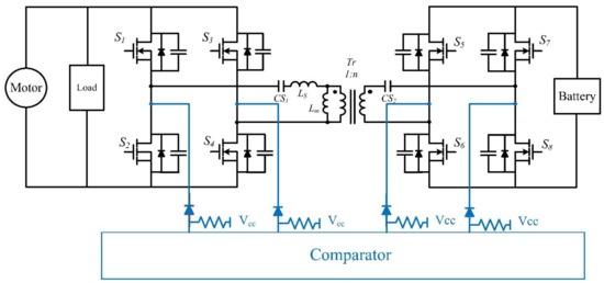
Figure 1.
The proposed adaptive SR driving scheme for the bidirectional LLC resonant converter.
2. Operating Principle of the Bidirectional Full-Bridge LLC Resonant Converter
This section will introduce the resonant tanks of bidirectional full-bridge LLC resonant converter. Since different designs of the resonant tanks will affect the characteristics of the transformer, which will pose a great impact on the charging and discharging modes, Severns proposed the design concepts of Type-4 and Type-11 resonant tanks, and the respective circuits are shown in Figure 2 below [19]. To achieve bidirectional energy conversion, Lu improved Type-4 and Type-11 resonant tanks and proposed modified Type-4 (MT-4) and modified Type-11 (MT-11) resonant tanks, respectively, as shown in Figure 3 below. The improved MT-4 and MT-11 enable soft switching [20].
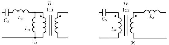
Figure 2.
Circuit diagrams of the Type-4 and Type-11 resonant tanks. (a)Type-4 LLC Resonant Tank; (b) Type-11 LLC Resonant Tank.
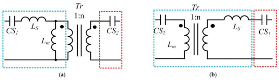
Figure 3.
Circuit diagrams of the MT-4 and MT-11 resonant tanks. (a)Type-4 LLC Resonant Tank; (b) Type-11 LLC Resonant Tank.
The circuit diagram of the bidirectional full-bridge LLC resonant converter is shown in Figure 4. This circuit comprises eight power switches (S1–S8) and a resonant tank. Lm is the self-inductance of the high-frequency transformer, Ls is the resonant inductance, and CS1 and CS2 are the resonant capacitances. The bidirectional LLC resonant converter operates in two modes: charging and discharging modes. In the charging mode, energy is transmitted from the primary side to the secondary side, with S1–S4 controlled by the gating signals of the main switches and S5–S8 controlled by synchronous rectification signals. In the discharging mode, energy is transferred from the secondary side to the primary side, with S5–S8 controlled by the gating signals of the main switches and S1–S4 controlled by synchronous rectification signals. The bidirectional full-bridge LLC resonant converter is capable of achieving soft switching, whether in the charging or discharging mode; this implies that both modes exhibit the characteristics of LLC resonance and, hence, additional energy buffering (snubber) is not necessary.
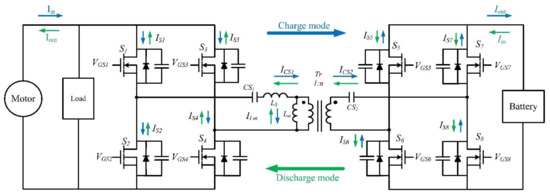
Figure 4.
Circuit diagram of the realized bidirectional full-bridge LLC resonant converter.
The following timing analysis was performed in the charging mode as an example, as the timing analysis of the discharge mode was similar to that of the charging mode.
The timing diagram of the bidirectional full-bridge LLC resonant converter using an MT-4 resonant tank is shown in Figure 5. Although MT-11 was also used as a design reference, it is not described herein because of space limitations. The timing diagram of the bidirectional full-bridge LLC resonant converter using an MT-4 resonant tank comprised eight states; however, because the first and second half-cycles were symmetrical, the analysis can be simplified to emphasize only the first half-cycle. The switching sequence in the charging mode is described below, whereas the operating states of the circuit are shown in Figure 6.
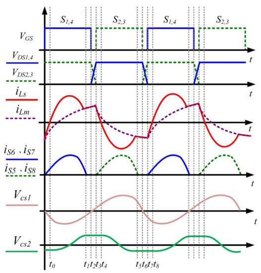
Figure 5.
The timing diagram of the bidirectional full-bridge LLC resonant converter using an MT-4 resonant tank.
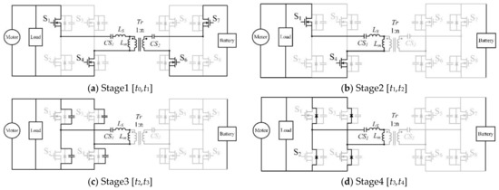
Figure 6.
The operating states of the bidirectional full-bridge LLC resonant converter using an MT-4 resonant tank. (a) Stage1 [t0,t1]; (b) Stage2 [t1,t2]; (c) Stage3 [t2,t3]; (d) Stage4 [t3,t4].
- (a) Stage1 [t0,t1]
During the time interval from t0 to t1, S1 and S4 were turned on. The resonant tank of the charging mode comprised CS1, LS, and CS2 connected in series, and the resonant current iLs exhibited a sinusoidal shape. Although the excitation current iLm increased, it resulted in resonance. On the secondary side, rectified currents iS6 and iS7, which flowed through S6 and S7, respectively, were proportional to the difference between iLs and iLm.
- (b) Stage2 [t1,t2]
When the resonant current iLs reached its peak value, it began decreasing gradually at a rate equivalent to the increase in the excitation current iLm starting from t1. As such, the rectified current on the secondary side was approximately zero, whereas S6 and S7 were switched off under ZVS. At resonance, the voltage on resonant capacitor CS2 reached its peak value, which did not change until resonance was attained again. The resonance among CS1, LS, and Lm on the primary side can be used to disconnect resonant capacitor CS2.
- (c) Stage3 [t2,t3]
Beginning from t2, S1 and S4 were turned off. iLs began charging parasitic capacitances of S1 and S4 and discharging parasitic capacitances of S2 and S3 simultaneously. At this stage, because the parasitic capacitances of the switches were smaller than that of the resonant capacitor CS1, the charging/discharging period of the former was shorter than that of CS1; therefore, the voltages of VdS1 and VdS4 increased quickly, whereas those of VdS2 and VdS3 decreased quickly. This stage ended when the VdS1 and VdS4 reached the input voltage, and the VdS2 and VdS3 became zero.
- (d) Stage4 [t3,t4]
When S2 and S3 were completely discharged, iLs flowed immediately through the body diodes of the two switches, and the energy was fed back to the input source. After t4, S2 and S3 were ready to be turned on under the ZVS condition. If the voltage on the magnetizing inductance Lm reaches the value of (V2-VCs2), then rectifier switches S5 and S8 are turned on to incorporate resonant capacitor CS2 again, causing resonance to occur on the primary side. The first half of the switching cycle ended after t4, and the second half of the switching cycle began.
2.1. Design Considerations
The original Type-4 and Type-11 bidirectional full-bridge LLC resonant converters share many similarities in terms of circuit characteristics and DC gain curve. The Type-4 full-bridge LLC resonant converter is regarded as a series–parallel resonance tank circuit with a bandpass filter, whereas the Type-11 full-bridge LLC resonant converter is regarded as a series–parallel resonance circuit developed based on an LS–CS series resonance converter. At resonance, the load is connected in parallel with the resonant element in the Type-11 LLC, whereas the load is connected in series with the resonant element in the Type-4 LLC. Therefore, at the resonance point, the DC gain of Type-11 will be greater than that of Type-4. The equivalent circuits of the bidirectional full-bridge LLC resonant converters using MT-4 and MT-11 resonant tanks are shown below in Figure 7. Equations (1) and (2) show the derived conversion ratio of MT-4 and MT-11, respectively.
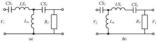
Figure 7.
Equivalent circuit of the bidirectional full-bridge LLC resonant converters using the (a) MT-4 and (b) MT-11 resonant tanks.
The following definitions were used in this study, where ωs is the switching frequency.
Equations (1) and (2) can be simplified to the following Equations (3) and (4):
Subsequently, the coefficients in Equations (3) and (4) are simplified as follows:
2.2. LLC Resonance Tank Design Procedure
To design MT-4 or MT-11 resonant tanks, four resonant elements must be taken into account simultaneously, which is considerably difficult. Hence, the general Type-4 or Type-11 resonant tank is designed first, followed by designing the additional resonant capacitors after the previous step is completed. MT-4 resonant tanks do not require a large DC gain; therefore, they are selected for the initial design, whereas MT-11 resonant tanks are used as a reference. The design procedure can be categorized into the following eight steps.
- (1)
- Determine the desired resonance frequency
- (2)
- Determine the parameter h. This parameter should be slightly large to accommodate a wide input design range.
- (3)
- The magnetizing inductance is calculated using the following equation:
- Tdead: total delay due to switching on/off, where Tdead = TON + TRise + TOFF + TFall; this value is typically between 100 and 500 ns.
- Fs: switching frequency
- COSS: parasitic capacitance of MOSFET
- (4)
- The values of LS, LM, and CS1 can be deduced based on Equations (5) and (6), substituting these values to calculate the DC gain. If the calculated DC gain does not satisfy the requirement, one must return to step 2) to reperform the design.
- (5)
- When Q1 reaches the maximum load, the DC gains of MT-4 can be calculated. Mathcad is used to draw the diagram. The value of g is selected when the DC gain curves satisfy the requirement and are closest to each other in the two modes, which can then be used for the design.
- (6)
- Based on the value of g, resonant capacitance CS2 can be calculated using g = CS2/CS1.
- (7)
- Verify whether the DC gain satisfies the load. If it does not, return to step 6) to obtain a new value of g.
- (8)
- Verify the value of the DC gain at the resonance frequency and substitute the value into the following equation to obtain the turn ratio n.
- (9)
- The design of the resonance tank is completed after step 8).
3. Description of the Proposed Adaptive SR Driving Strategy
This section will give an introduction of the proposed adaptive SR driving strategy. The desired SR gate driving signals in different switching frequency regions will be distinct; hence, proper tuning of the SR gate driving scheme within all switching frequency regions is essential. When the main switch on the primary side is turned on, current flows through the SR switch on the secondary side. At this time, the SR switch should be turned on. Nevertheless, the timing to turn off the SR switch is not necessarily when the main switch is turned off. When the switching frequency is less than the resonance frequency (Fsw < Fo), the SR switch must be turned off earlier than the main switch; otherwise, energy will be returned from the secondary side to the primary side. When the switching frequency is greater than the resonance frequency (Fsw > Fo), the SR switch should be turned off later than the main switch; otherwise, the rapidly decreasing current will flow through the body diode, and the recovery current in the reverse direction will result in poor efficiency. Figure 8 below shows the following three scenarios: (a) when the SR switch is turned off long before the main switch, (b) when the SR switch is turned off slightly before the main switch, and (c) when the SR switch is turned off with the main switch.
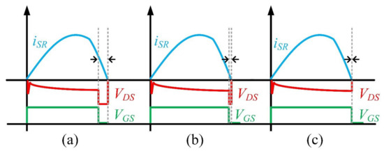
Figure 8.
Concepts of different timing to turn off the SR switch (a) long before the main switch, (b) slightly before the main switch, and (c) with the main switch.
Figure 9 shows the relationship between the drain to source voltage and the comparator outputs. As the switching frequency of the drive signal is high, the output VComparator from the comparator is a high-frequency signal. If noise is present, misjudgments may occur. Therefore, two methods are proposed herein to determine the amount of PWM width that must be adjusted in response to noise. As shown in Figure 10 below, the first method uses ECAP to calculate the upper and lower limits of the trigger event and record the time interval between Event1 and Event2 (Event1-Event2). As the PWM signal is calculated and output by the DSP, the PWM period will be equal to the value stored in the PRD (Period Register). The second method uses ECAP to record the time from Event1 to Event4 (Event1-Event4) and then subtracts the PRD to obtain . The obtained by these two methods must be the same for it to be applicable for minimizing misjudgments caused by noise.
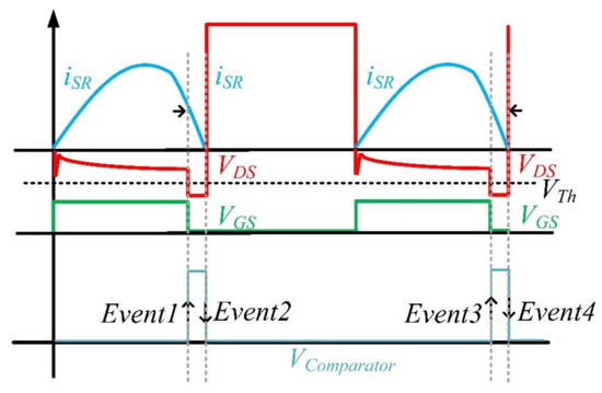
Figure 9.
Relationship between VComparator and Vds.
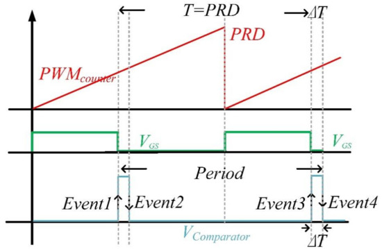
Figure 10.
Concepts of minimizing the misjudgement.
The TMS320F28027 used in this study is a low-cost DSP manufactured by Texas Instruments, and the event capture module is dedicated to detecting the upper and lower limits of an event only. Unlike mid-to-high-priced DSPs, which have multiple ECAPs, TMS320F28027 has only one ECAP; therefore, a digitally controlled multiplexer should be utilized to monitor all four channels, as shown in Figure 11 below. The multiplexer can adjust the timing to use the four channels. Utilizing this method, it can detect the states of the four channels of the synchronous rectifier even with only one ECAP. The outputs from the four comparators are used as the input signals of the multiplexer, and the output of the multiplexer is connected to an open collector circuit. Subsequently, the signals will be sent to the ECAP of the DSP for detection.
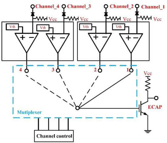
Figure 11.
The proposed multiplexer circuit.
4. Realization of the Proposed Adaptive SR Driving Strategy
This section will firstly present the realization of the proposed adaptive SR driving strategy using microcontrollers; next, the two subroutines designed in this study will be introduced. This article completes the adaptive function with two subroutines, Channel Select and SR Tuning; the flowchart of the Channel Select subroutine is shown in Figure 12. The primary function of the Channel Select subroutine is to determine the required multiplexer channels and sequentially sample signals in accordance with the converter’s operating modes. When entering the Channel Select subroutine, it should be judged whether it is in the charging mode or the discharge mode; then, operating the multiplexer with the corresponding charging mode or discharge mode by selecting Channel 1, 2, 3, or 4. Last, record the VRds voltage output of Q2, Q4, Q6, and Q8 and call the SR Tuning subroutine.
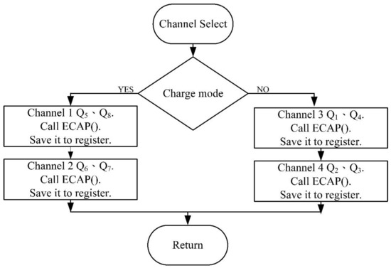
Figure 12.
Flowchart of the Channel Select subroutine.
As illustrated in the timing diagrams shown in Figure 5. Providing that the duty cycle is too small in the SR switches, i.e., the SR switches is turned off at t1, the body diode of the SR switches will conduct, which will reduce the converter’s efficiency. Therefore, the SR switches’ duty cycle must set a lower limit to prevent inefficiency caused by the smaller SR switches’ duty cycle. However, supposing that the SR switches’ duty cycles are too large, as Figure 5 shows, the SR switches’ duty cycles are greater than tmain + tdead. In that case, a short circuit will occur between the upper and lower arms in the period from t2 to t3. As a result, SR switches should limit the duty cycle’s upper limit as tmain + tdead to prevent short circuits. Figure 13 and Figure 14 show the lower limit and the upper limit of the SR switches, respectively.
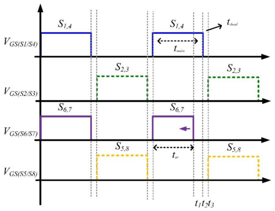
Figure 13.
Lower limits of the SR switches.
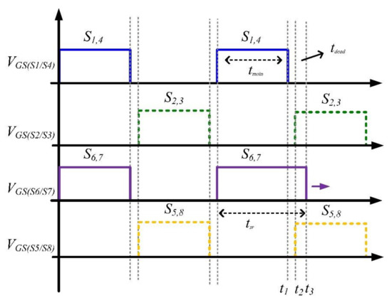
Figure 14.
Upper limits of the SR switches.
Taken into account the abovementioned limitations, this article proposes the SR Tuning subroutine to reach the highest efficiency by calculating and adjusting the switching sequence of synchronous rectification. When entering the subroutine, the comparator’s voltage should be checked first, judging whether it requires the adjustment of the switching sequence or not. If the comparator’s output is low, subtract ∆D from the SR switches’ duty cycles (Tsr). Then, judging whether the SR switches’ duty cycles are lesser than the lower limit (tmin) or not. If yes, limit its minimum as the lower limit. On the other hand, if the comparator’s output is high, save Period1 and Period2. Period1 is T1 (period of Event1-Event4) minus Period Register (PRD); Period2 is ∆T (period of Event1-Event2). Next, judging whether the value of Period1 and Period2 are equal. The two values would be equal without noise interference; when the values are unequal, this adjustment should be abandoned. If there is no noise interference, judge whether Tsr is greater than the constraint condition tmain + tdead. If yes, limit Tsr to tmain + tdead to prevent short circuits between the upper and lower arms. If Tsr is not greater than the constraint condition, add up the SR switches’ duty cycles with ∆D, as shown in Figure 15.
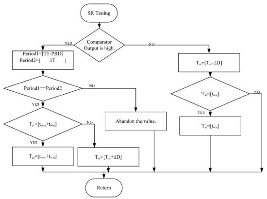
Figure 15.
Flowchart of the proposed SR Tuning subroutine.
5. Experimental Results
This section will perform the functional verification of the proposed converter based on the theory mentioned in Chapters 2 and 3, as well as the software design in Chapter 4. This study uses the YOKOGAWA WT500 power analyzer for measurement; the measurement accuracy of WT500 is ±0.1%, ensuring the measurement reliability. In this study, a 60 W bidirectional full-bridge LLC resonant converter with synchronous rectification was designed with an input voltage of 24 V and an output voltage of 12 V. The parameters of the circuit are shown in Table 1, and Figure 16 shows the realized prototyping circuit of the proposed bidirectional full-bridge LLC resonant converter. The DSP used in this study is manufactured by Texas Instruments, Texas, USA. The comparator circuit collects the Vds voltages on the primary and secondary sides, compares them with Vth using the comparator, and returns the results to the DSP for processing.

Table 1.
Converter specification and designed parameters.
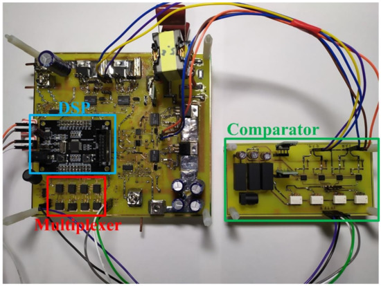
Figure 16.
Photograph of the proposed circuit.
Figure 17 shows that the gating signal of the main switches contains a 300 ns deadtime to prevent the switches from being turned on simultaneously and resulting in a short-circuit. In the charging and discharging modes, the 300 ns deadtime is fixed on the primary and secondary sides, respectively.
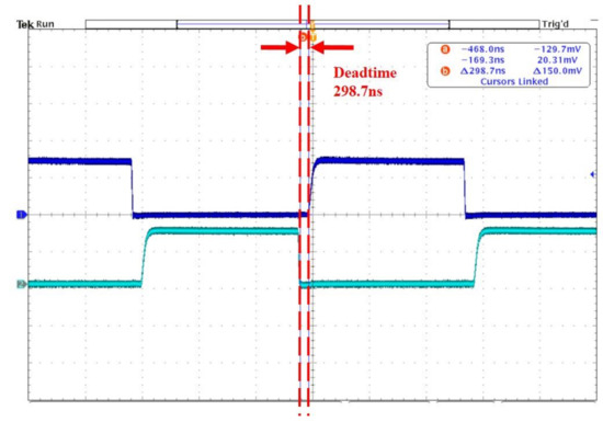
Figure 17.
Waveforms of the gating signal on the primary side showing the deadtime interval.
Figure 18 shows the ZVS waveforms of the power switch at a light load (1 A) and full load (5 A). As shown in the figure, the converter can achieve ZVS at a light load to attain high efficiency.
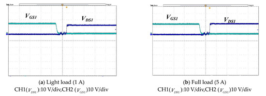
Figure 18.
Zero-voltage switching waveforms: (a) light load, (b) full load.
As shown in Figure 19, when the switch is turned on, the voltage on the switch is calculated by multiplying the current through the switch with the on-resistance. As Rds(on) is extremely small, the voltage on the switch differs significantly from that when current flows through the body diode. When the SR switch is turned off at t1, the current changes its path and flows through the body diode, and the voltage on Rds decreases further. The comparator detects this phenomenon, generates an output, and provides it to the DSP for calculation.
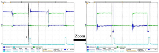
Figure 19.
Waveforms of the SR driving signals without the proposed technique.
As shown in Figure 20, with the proposed adaptive SR driving technique, the PWM width is adjusted. It is clear that the new PWM width is more suitable, and the comparator output no longer detects the phenomenon wherein the current passes through the body diode because the switch is turned off early.
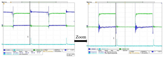
Figure 20.
Waveforms of the SR driving signals with the proposed technique.
Figure 21 shows the measured efficiency curves of the charging and discharging modes, respectively. The highest efficiency of the charging mode reached 93.35%, whereas the largest difference in efficiency between the conventional SR driving technique and the proposed one under the charging mode is 1%, with an average of 0.462% improvement. On the other hand, the highest efficiency of the discharging mode is 95.82%, which differs at most by 1.65% from that of the conventional SR driving method, with an average of 1.097% improvement.
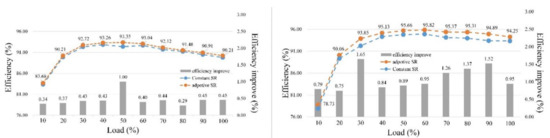
Figure 21.
Efficiency curves.
6. Conclusions
This study firstly introduced the design of the bidirectional full-bridge LLC resonant converter and the challenges it faced. Next, this study designed a resonant tank applicable for bidirectional structures and proposed the adaptive SR driving strategy. In this study, the design of an adaptive SR of a bidirectional full-bridge LLC resonant converter was performed. The drain to source voltage on the SR switch was observed and subsequently sent to a comparator for comparison, and the PWM width of the SR switch in the charging and discharging modes was adjusted accordingly. When the proposed adaptive SR driving scheme is used, the body diode conduction is eliminated by the tuning of the SR turn off time. The SR gate driving signal is allowed to be tuned within all operating frequency regions. Furthermore, the introduction of a simple digital implementation is explained. The sampling from four channels can be sent to the DSP through a custom-made multiplexer circuit, enabling the realization of the proposed technique using a low-cost DSP that comprised only one ECAP module. The efficiency reached up to 95.82%, with a 1.65% improvement when compared with the conventional bidirectional full-bridge LLC resonant converter.
Author Contributions
This research article has five authors. S.-C.W. and Y.-H.L. conceived the research method and designed the control strategy. C.-Y.L. constructed the prototyping circuits and performed the experiments. Z.-Z.Y. and S.-P.Y. analyzed the resulting data and wrote the manuscript. All authors have read and agreed to the published version of the manuscript.
Funding
This research received no external funding.
Institutional Review Board Statement
Not applicable.
Informed Consent Statement
Not applicable.
Data Availability Statement
The data presented in this study are available on request from the corresponding author.
Conflicts of Interest
The authors declare no conflict of interest.
References
- Mohan, N.; Undeland, T.M.; Robbins, W.P. Power Electronics: Converters, Applications and Design, 3rd ed.; John Wiley & Sons: New York, NY, USA, 2003. [Google Scholar]
- Liu, K.H.; Lee, F. Zero-voltage switching technique in DC/DC converters. IEEE Trans. Power Electron. 1990, 5, 293–304. [Google Scholar] [CrossRef]
- Chen, W.; Ruan, X.; Zhang, R. A Novel Zero-Voltage-Switching PWM Full Bridge Converter. IEEE Trans. Power Electron. 2008, 23, 793–801. [Google Scholar] [CrossRef]
- Yau, Y.T.; Hwu, K.I.; Shieh, J.J. Simple Structure of Soft Switching for Boost Converter. Energies 2020, 13, 5448. [Google Scholar] [CrossRef]
- Kollipara, N.; Kazimierczuk, M.K.; Reatti, A.; Corti, F. Phase control and power optimization of LLC converter. In Proceedings of the IEEE International Symposium on Circuits and Systems, Sapporo, Japan, 26–29 May 2019; pp. 1–5. [Google Scholar]
- Park, H.P.; Kim, M.; Jung, J.H. A Comprehensive Overview in Control Algorithms for High Switching-Frequency LLC Resonant Converter. Energies 2020, 13, 4455. [Google Scholar] [CrossRef]
- Lin, B.R. Analysis of a Series-Parallel Resonant Converter for DC Microgrid Applications. Processes 2021, 9, 542. [Google Scholar] [CrossRef]
- Luo, J.; Wang, J.; Fang, Z.; Shao, J.; Li, J. Optimal Design of a High Efficiency LLC Resonant Converter with a Narrow Frequency Range for Voltage Regulation. Energies 2018, 11, 1124. [Google Scholar] [CrossRef]
- Kim, D.H.; Kim, M.S.; Nengroo, S.H.; Kim, C.H.; Kim, H.J. LLC Resonant Converter for LEV (Light Electric Vehicle) Fast Chargers. Electronics 2019, 8, 362. [Google Scholar] [CrossRef]
- Cai, G.; Liu, D.; Liu, C.; Li, W.; Sun, J. A High-Frequency Isolation (HFI) Charging DC Port Combining a Front-End Three-Level Converter with a Back-End LLC Resonant Converter. Energies 2017, 10, 1462. [Google Scholar] [CrossRef]
- Yan, X.; Li, J.; Zhang, B.; Jia, Z.; Tian, Y.; Zeng, H.; Lv, Z. Virtual Synchronous Motor Based-Control of a Three-Phase Electric Vehicle Off-Board Charger for Providing Fast-Charging Service. Appl. Sci. 2018, 8, 856. [Google Scholar] [CrossRef]
- Xie, X.; Liu, J.C.P.; Poon, F.N.K.; Pong, M.H. A novel high frequency current-driven SR applicable to most switching topologies. IEEE Trans. Power Electron. 2001, 16, 635–648. [Google Scholar]
- Wang, P.; Cui, G.; Chen, L. Analysis and design of LLC with new current driven synchronous rectifiers. In Proceedings of the International Conference on Electrical and Control Engineering, Yichang, China, 16–18 September 2011; pp. 4344–4347. [Google Scholar]
- Huang, D.; Fu, D.; Lee, F.C. High switching frequency, high efficiency CLL resonant converter with synchronous rectifier. In Proceedings of the 2009 IEEE Energy Conversion Congress and Exposition, Institute of Electrical and Electronics Engineers (IEEE), San Jose, CA, USA, 20–24 September 2009; pp. 804–809. [Google Scholar]
- Zhang, G.; Zhang, J.; Chen, Z.; Wu, X.; Qian, Z. LLC resonant DC/DC converter with current-driven synchronized volt-age-doubler rectifier. In Proceedings of the IEEE Energy Conversion Congress and Exposition, San Jose, CA, USA, 20–24 September 2009; pp. 744–749. [Google Scholar]
- Wu, X.; Hua, G.; Zhang, J.; Qian, Z. A new current-driven synchronous rectifier for series–parallel resonant (LLC) DC-DC converter. IEEE Trans. Ind. Electron. 2011, 58, 289–297. [Google Scholar] [CrossRef]
- Wu, X.; Li, B.; Qian, Z.; Zhao, R. Current driven synchronous rectifier with primary current sensing for LLC converter. In Proceedings of the IEEE Energy Conversion Congress and Exposition, San Jose, CA, USA, 20–24 September 2009; pp. 738–743. [Google Scholar] [CrossRef]
- Feng, W.; Lee, F.C.; Mattavelli, P.; Huang, D. A Universal Adaptive Driving Scheme for Synchronous Rectification in LLC Resonant Converters. IEEE Trans. Power Electron. 2012, 27, 3775–3781. [Google Scholar] [CrossRef]
- Severns, R. Topologies for three-element resonant converters. IEEE Trans. Power Electron. 1992, 7, 89–98. [Google Scholar] [CrossRef]
- Chen, W.; Rong, P.; Lu, Z. Snubberless Bidirectional DC–DC Converter With New CLLC Resonant Tank Featuring Minimized Switching Loss. IEEE Trans. Ind. Electron. 2010, 57, 3075–3086. [Google Scholar] [CrossRef]


Publisher’s Note: MDPI stays neutral with regard to jurisdictional claims in published maps and institutional affiliations. |
© 2021 by the authors. Licensee MDPI, Basel, Switzerland. This article is an open access article distributed under the terms and conditions of the Creative Commons Attribution (CC BY) license (https://creativecommons.org/licenses/by/4.0/).