1. Introduction
The everlasting development of renewable generation systems brings about a potential challenge to the stability of grid, since the balance between electrical energy providers and consumers recently becomes much harder to be maintained [
1,
2]. In such a context, energy storage technology is believed to be one of the best choices to solve this problem [
3]. Battery energy storage system (BESS), characterized by its high energy density, high efficiency, flexibility and fast response, is highly suitable to perform as an energy buffer in renewable generation applications [
3,
4]. As a result, the research about BESS is rapidly gaining more and more attentions in recent years.
Power conversion system (PCS), which can be classified to a dedicated kind of grid-tied converter, is the intermediate power electronics equipment between battery packs and grid. Its main task is to transfer the electrical energy stored in the battery packs bi-directionally to the grid through semiconductor switches and a passive low-pass filter [
5,
6]. Benefit from its lower cost and better high frequency suppression performance, PCS usually contains an LCL filter to attenuate the high frequency ripples generated by the switching process of power devices. However, the inherent resonance feature also leads to stability issue in evidence. To deal with this problem, additional damping method needs to be adopted and a lot of related researches have been done so far for decades.
Passive damping is the simplest way to stabilize LCL filter by adding extra resistors in the circuit. Although this scheme is effective and easy to implement, additional power loss and increased cost restrict its further applications [
7,
8,
9]. By properly changing the circuit structure, a series of modified high-order filter, such as LLCL filter, can be obtained. It is believed that the frequency domain feature of these filter topology is improved but the resonance peak is still difficult to be totally eliminated [
10,
11]. Therefore, active damping (AD) techniques are taken into account by feeding back specified variables (single variable or combination of variables) inside the filter or embedding an internal digital filter into the controller to modify the forward path [
12]. Because AD only needs to change the control loop in the processor without introducing additional components, it becomes more preferable than passive damping techniques now.
L. Zhou et.al combined a first-order high-pass filter with converter-side current feedback loop in [
13] for distributed generation system. The analysis in [
13] shows that this is equivalent to create a virtual impedance connected with the converter-side inductor in series, which is helpful to suppress the original resonance peak with a reduced frequency offset. Literature [
14] proposed a novel AD algorithm based on negative resonance regulator and grid-current feedback. The outstanding advantages of this algorithm includes lower switching noise sensitivity and superior control delay compensation. The performance of inverter was also tested while connecting to a weak grid. Ref. [
15] embedded a digital notch filter implemented based on direct-form II transposed in the controller to tackle the resonance issue caused by the uncertain parameter drift of main circuits. It is found that this AD strategy tolerates the resonance frequency drifting well by sufficient experimental verifications. In [
16], a hybrid AD algorithm based on capacitor current feedback and point of common coupling voltage feedback was proposed. The cooperation between these two individual feedback channels can provide the maximum profit to ensure the robustness of AD in cases parameter variation and non-ideal grid takes place. Similar damping requirement is also significant for stand-alone inverter applications. The authors in [
17] employed a selective frequency scheme which localized the influence scope of AD loop only near the resonance frequency; thus, the inverter’s feature in other frequency range stayed the same to provide better steady and dynamic performances.
For another aspect, disturbances and uncertainties are inevitable in most practical industrial applications. These unfavorable factors usually cause performance degradation. To combat this issue, disturbance/uncertainty estimation and attenuation has become a long-lasting topic both in academia and industry since early 1960s [
18]. This technique is a powerful tool for optimizing the trade-off process between disturbance rejection and rapidity, steady-state performance and robustness of the closed-loop controlled object. Within the related engineering fields, a lot of implementing approaches have been proposed.
Literature [
19] designed and implemented a novel controller combined with traditional feedback loops and disturbance observer (DOB) based control. The key advantage of this controller is that it can maintain the original fast dynamic response achieved by feedback control even in the presence of external perturbation and model mismatch. Literature [
20] proposed a control strategy based on active disturbance rejection control by selecting grid-side current as the unique feedback signal. The inverter possesses stronger robustness against parameter fluctuation after the adoption of extended state observer which can mathematically transforms the inverter downgrade to a simple gain module. Similarly, Ref. [
21] proposed a simplification method to achieve order reduction for the plant transfer function of LCL filter by utilizing Pade approximation and extended state observer. Furthermore, DOB has been integrated with other control methods such as finite set model predictive control [
22]. In [
23], DOB was also applied to a grid-tied converter based on five-level T-type AC-DC topology to improve its disturbance rejection capability towards dc-bus load variation. Stability improvement of DC-DC converter can also be achieved by properly introducing DOB [
24]. These cases prove that DOB is widely applicable. Therefore, an AD control strategy based on DOB for PCS is presented as an enhancement of stability and robustness in this paper.
The subsequent part of this paper is organized as following:
Section 2 describes the basic principle of AD for LCL filter and implementation of DOB.
Section 3 discusses the parametric design and stability issue of the observer.
Section 4 establishes the simulation model in the environment of Matlab/Simulink. Simulation results are provided in this section. Prototype is constructed and
Section 4 also introduces the experimental results. Finally,
Section 5 concludes the paper.
2. Principle of Active Damping Control and Disturbance Observer
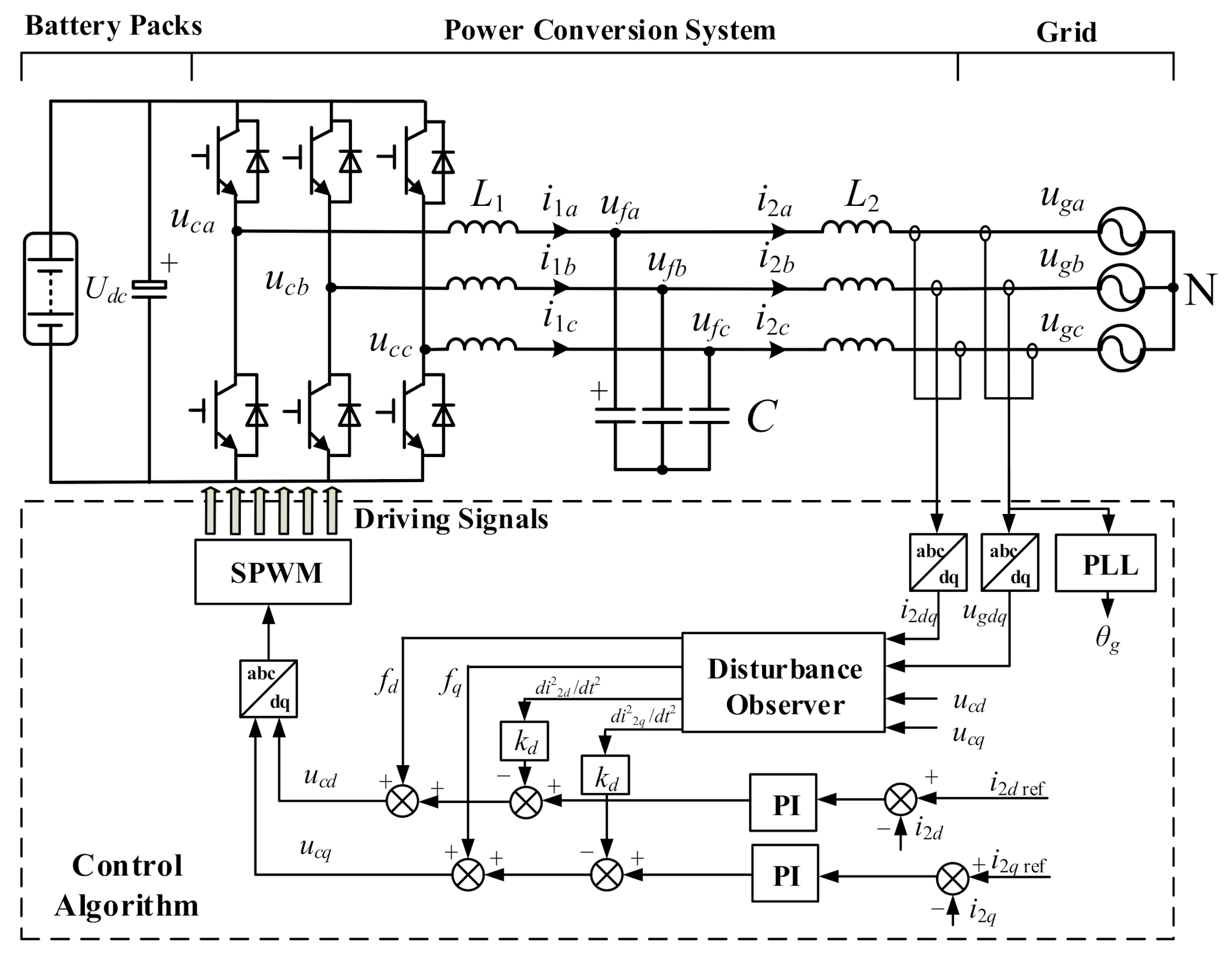
Figure 1 briefly illustrates the block diagram and control principle of PCS on basis of a widely-used two-level voltage source converter. The DC terminals of PCS are connected to the battery packs which perform as the main static energy storage components in the BESS. Within a relatively short time scale, the output voltage of battery packs, denoted as
Udc, can be assumed to be constant. Meanwhile the AC terminals of PCS are connected to a standard three-phase three-wire grid. With sinusoidal pulse width modulation technology and grid voltage-oriented vector control, the PCS is capable of transferring AC energy from the grid to dc energy stored in the battery packs and vice versa in order to manage charging or discharging power flexibly and quickly according to the upstream grid instructions. LCL filter is used to attenuate the high order harmonic generated by the PCS.
For ease of description, In
Figure 1,
L1 represents the converter-side inductor,
C is the filter capacitor,
L2 represents the grid-side inductor, these passive components formed a three-order LCL filter together. The parasitic resistances of
L1 and
L2 are defined as
R1 and
R2 respectively. The output voltages per phase leg are denoted as
uca,
ucb and
ucc. Converter-side currents are denoted as
i1a,
i2b and
i2c. Grid-side currents are represented by
i2a i2b and
i2c. Instantaneous voltages of filter capacitors are
ufa,
ufb and
ufc. Three-phase grid voltage are represented by
uga,
ugb and
ugc. The subscripts a–c represent the phase sequence respectively. The grid-side power is the ultimate control target of PCS. By adjusting
i2d and
i2q, active power and reactive power can be adjusted separately.
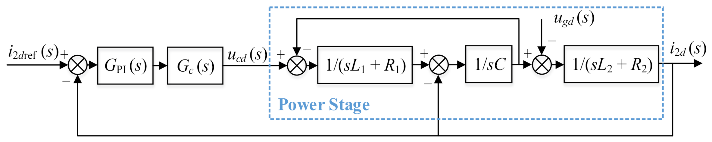
By applying dq-transformation, the grid-tied PCS can be modelled and separated into two subsystem, d-axis and q axis subsystems, in the synchronous rotating frame. The angle for dq-transform is calculated according to grid voltage by a phase locked loop (PLL). The coupling term between these two subsystems can be regarded as the internal disturbance and assumed to be ignorable at first, the block diagram of control loop for d-axis subsystem is given in
Figure 2.
Meanwhile, the q-axis subsystem has the identical structure as
Figure 2. Therefore, only d-axis subsystem is necessary to be discussed. Proportional integral (PI) regulator is usually selected to be inserted in the forward path in order to handle the closed-loop control of i
2d and i
2q. The transfer function of
GPI (s) equals to
where
kp and
ki are the proportional and integral coefficient of PI controller.
Gc (s) represents the model of the voltage source converter, which can be approximated to the form of Equation (2) by neglecting modulation and sampling delay, where
KPWM is the modulation coefficient and
Utri is the carrier amplitude in SPWM module.
Then, the original frequency domain characteristics of LCL filter can be described by Equation (3)
Usually, the parasitic resistance is very small in practice and can be ignored. Obliviously, there are three poles in the system. One pole locates at the origin point of complex plane and the other two poles locate conjugatively on the imaginary axis, which means the system tends to oscillate with the resonance frequency
fr depicted in Equation (4). This is not acceptable for most industrial applications.
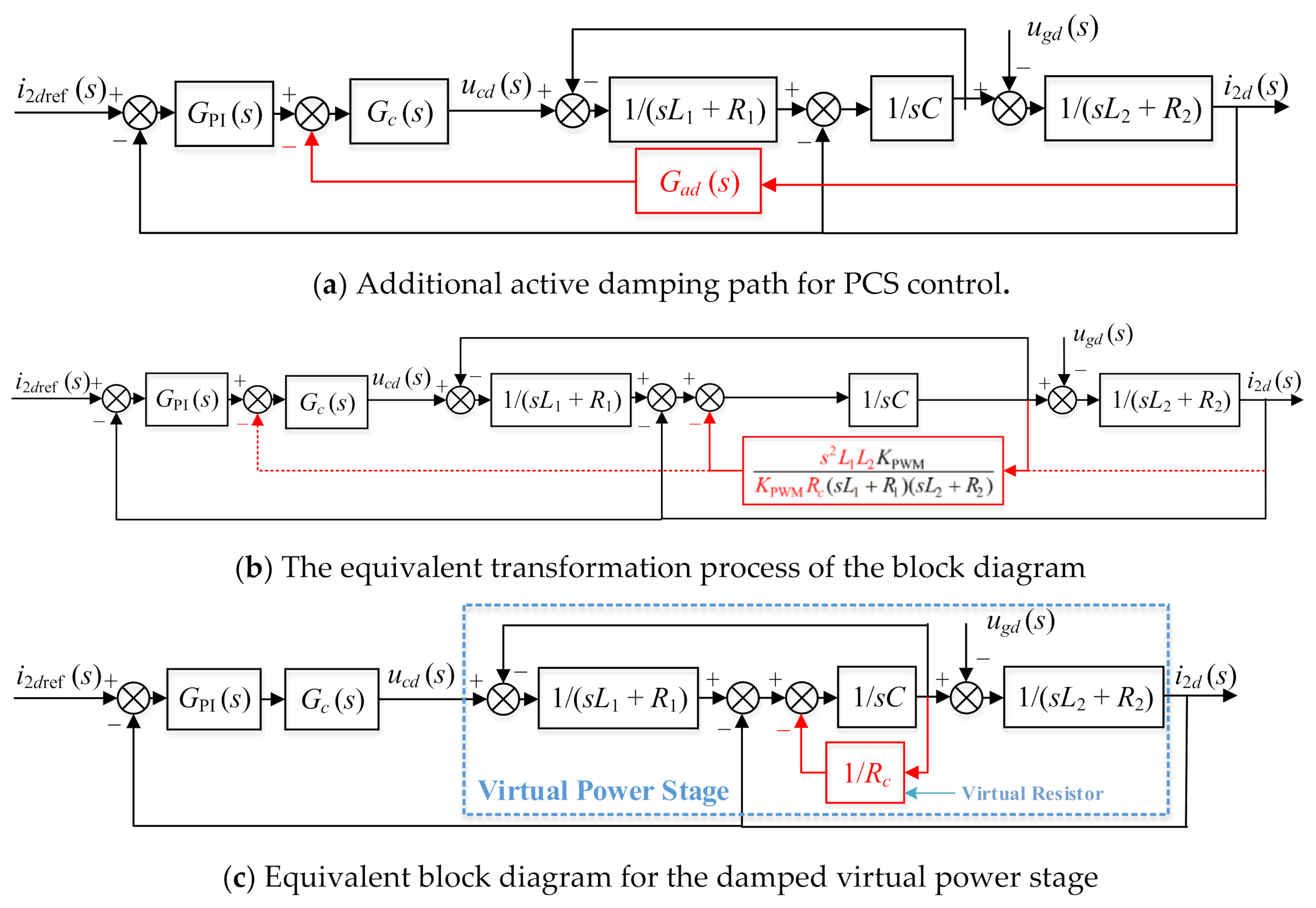
Therefore, it is necessary to adopt either active or passive damping methods to attenuate the resonance peak of LCL filter for purpose of guaranteeing the stability of PCS. AD method is usually preferable since it avoids additional power loss and passive components. To achieve AD, it is possible to reconfigure the control loop by adding a feedback branch from
i2 to
uc. The equivalent transfer function of PCS’s power stage can be changed to the desired form after properly setting
Gad(
s) as
After involving the additional AD path, the equivalent block diagram can be simplified from
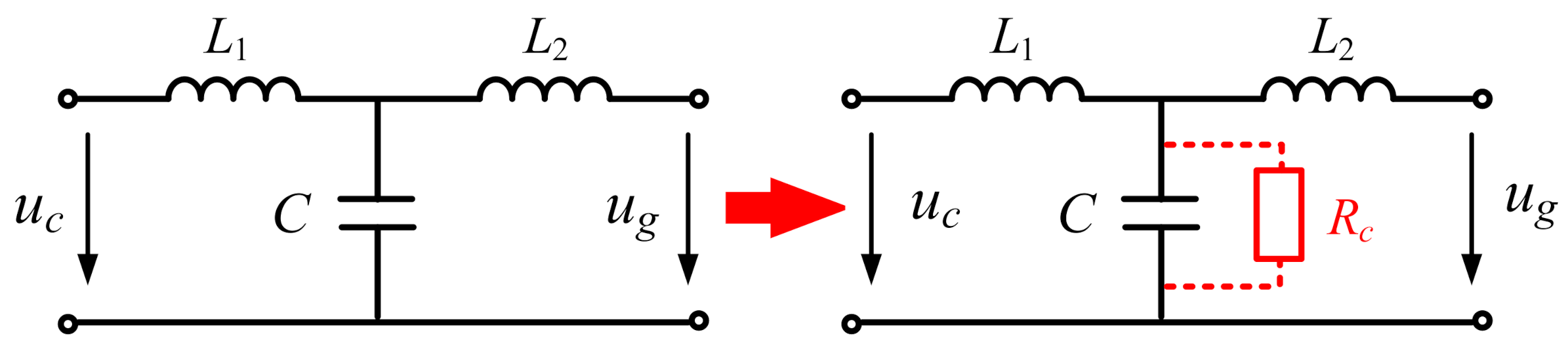
Figure 3a–c. According to the modified block diagram, it can be found that adding
Gad(
s) in the control loop has the same effect as connecting a virtual resistor
Rc in parallel with filter capacitor which can be described by
Figure 4. The LCL circuit is converted to an LCRL circuit.
The value of virtual resistor equals to the control parameter
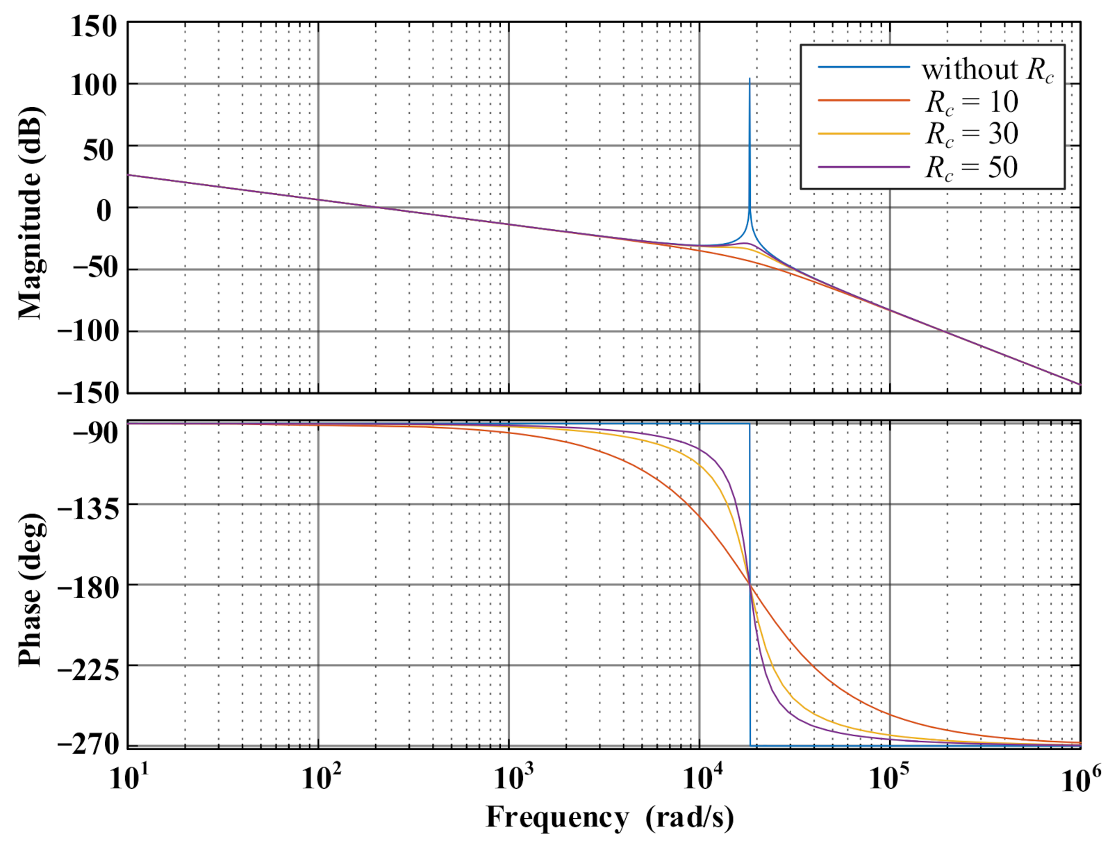
Rc. Therefore, it is much easier to be adjusted compare to traditional passive damping method. The corresponding bode diagram is shown in
Figure 5 as a comparison for different
Rc values. It can be seen according to
Figure 5 that the resonance of the LCL filter is effectively suppressed after adding the above feedback branch for AD. In addition, when the damping resistance increases, the resonance suppression effect will be weakened.
However, the anti-interference ability of PCS tends to be poor due to the adoption of the second-order derivation of grid-injected current. The noise of sampling circuit and current sensors both become potential threats to the stability and accuracy of control method. The direct calculation of
d2i2d/
dt2 and
d2i2q/
dt2 and is difficult to be achieved and this is assumed to be the main drawback of AD method depicted in
Figure 3a. On the other hand, the output voltage is not accurate due to the non-ideal features of power switches and inevitable dead band. Moreover, the firstly omitted coupling effect between d-axis and q-axis subsystems can also be regarded as an unknown disturbance. In order to solve these problems, this paper presents a DOB to estimate
d2i2d/
dt2 and
d2i2q/
dt2 together with the unmeasurable disturbances denoted as
fd and
fq. Based on the observer, the disturbances are possible to be compensated by subtracting
fd and
fq from the reference voltages
ud and
uq, respectively. According to
Figure 2, Equation (6) can be derived as
The first and second order differential terms of the grid voltage in Equation (6) can also be included in the disturbance quantity, the right-side of Equation (6) represents the control variables which contains unknown disturbances. By rewriting Equation (6) in the form of differential equations set, we can obtain Equation (7).
To simplify the expression, let
According to Equation (7), we can properly select the state space
x = [
x1 x2 x3 x4 x5 x6 x7 x8]
T, which is further defined in Equation (9) to construct the mathematical model of PCS.
These state variables can be regarded as constants in steady state in the dq reference frame. On the basis of this assumption, state space model can be further derived as
Rewrite Equation (10) into the standard matrix form
where
The observability of system should be checked first. Thus, the rank of observability judgment matrix N is calculated.
According to the calculation result in Equation (13), it can be found that N is full ranked. Therefore, it is feasible to construct an observer to estimate
d2i2d/
dt2,
d2i2q/
dt2,
fd and
fq. Full state observer and dimensionality reduction observer are both good choices for state estimation. In this paper, full state observer is selected because of its better stability performance. The DOB is established in Equation (14)
where
represents the estimated value of
x. The feedback matrix
M performs a correction function to the DOB, it can be expressed as
where
g1,
g2 are parameters to be determined, which decide the pole distribution and the stability of observer. Then, Equation (14) is discretized to Equation (16) based on explicit Euler method. Define
Ts as the sampling period,
where
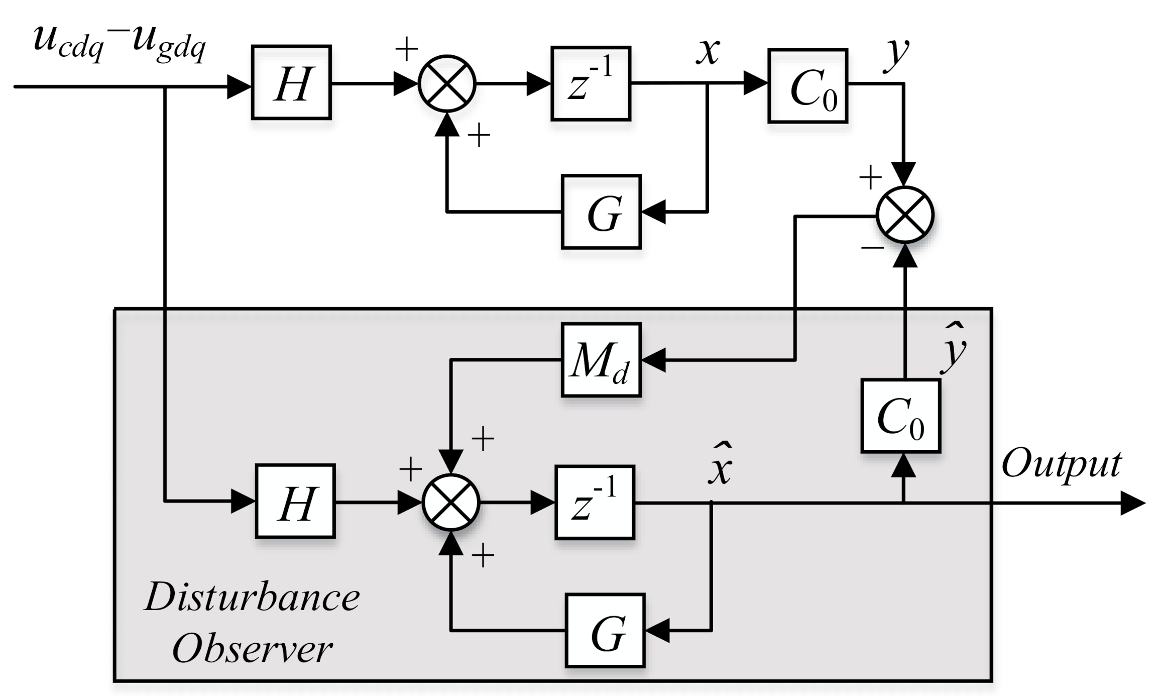
Finally, as a summary, the signal flow diagram of DOB is shown in
Figure 6, which aims to depict the relationship between the actual and observed value of PCS. The observer takes the difference between the converter output voltage and the grid voltage as the input and uses the error between actual grid-side current and the observed current as the feedback correction, so that the observer state variables are possible to converge to the realistic system variables. Then, the observed values of disturbances and second-order differential of grid-side current are obtained. Moreover, in the next section, stability analysis and design of Matrix
M will be discussed in detail.
3. Stability Analysis and Parametric Design of the Disturbance Observer
The performance and stability of DOB highly rely on the parametric design of feedback matrix. If the initial estimation error of
x is defined as Δ
x(0), after
k periods iteration, the final observing error Δ
x(
k) can be expressed as
Therefore, it can be deduced that the stability and convergence of DOB is determined by the eigenvalue of
G−
MdC0. For theoretical analysis afterwards, the parameters of main circuit can be referred to
Table 1 in
Section 3.
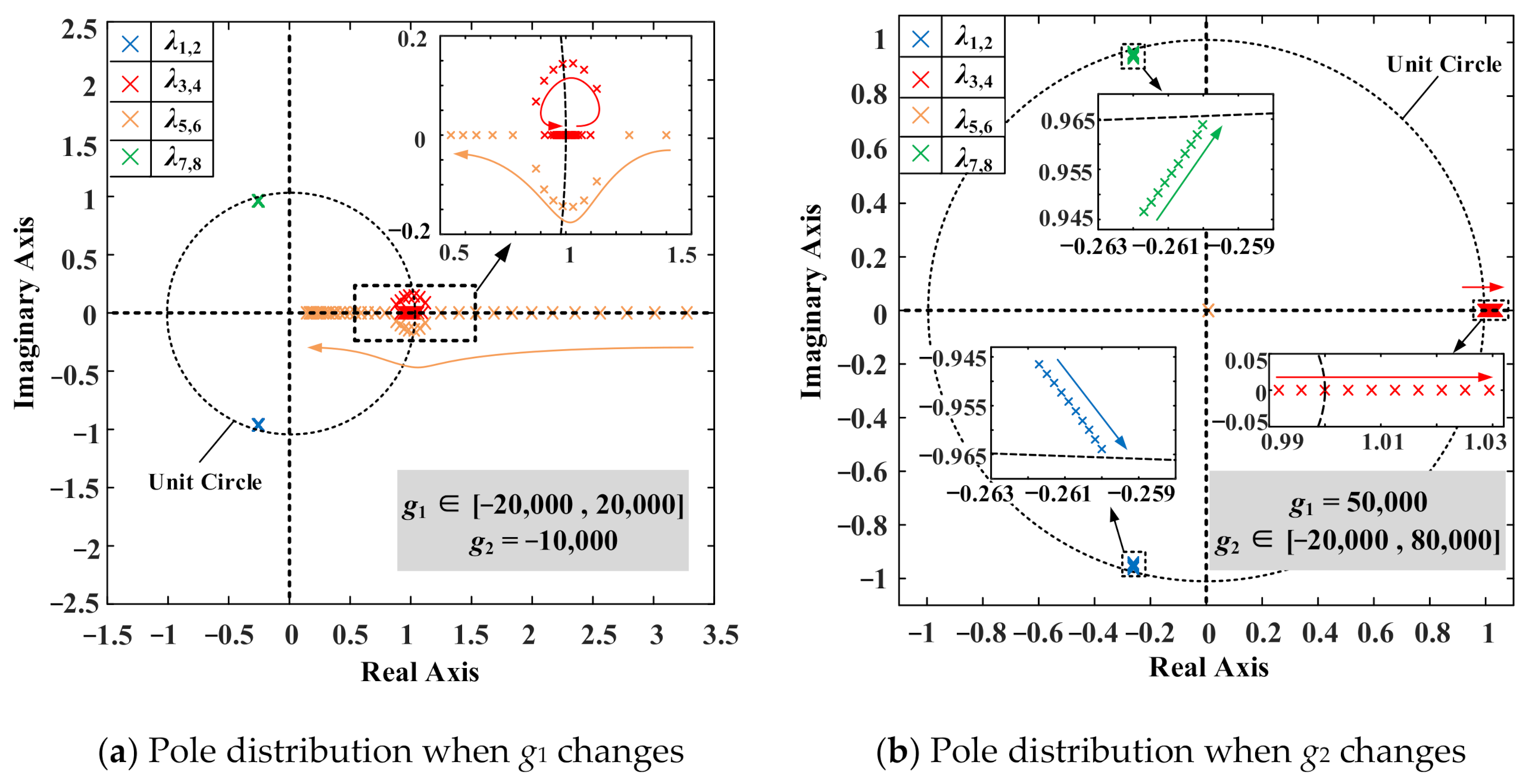
Figure 7 shows the locus of the eigenvalue distribution of the matrix
G−
MdC0 when
Md changes. It is worth nothing that the observer presented in this paper has a simplified process of ignoring the internal coupling term of the d and q axis when modeling, so it can be considered that the d axis and q axis are dependent with each other and have a completely symmetric characteristic eigenvalue distribution.
It can be seen from
Figure 7 that the closed-loop observer has eight poles in total.
λ1~
λ8 represent all the eigenvalues of matrix
G-
MdC0. When
g1 and
g2 are both negative, we can see from
Figure 7a that the system has a pole on the right side of z-plane which is far away from the unit circle. The observer is unstable in this situation. In the process of changing
g1 from negative to positive numerically, this pole can gradually approach and, finally, enter into the unit circle. It means that
g1 should be greater than zero when
g2 is negative.
Figure 7b shows the locus of the poles distribution when
g1 is positive and
g2 changes from negative to positive numerically. The poles move from the inside towards the outside of the unit circle, which means the observer tends to be unstable. As a brief conclusion, the parameters
g1,
g2 directly affect the stability and performance of DOB; thus, their values must be designed carefully.
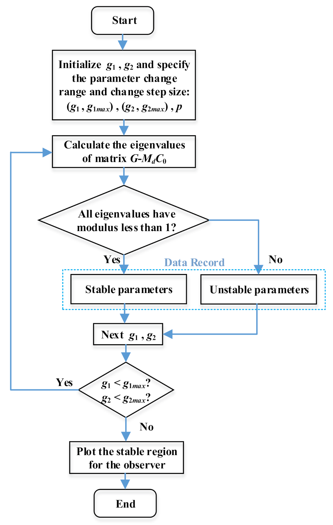
However, the order of synthesized matrix equals to eight. Therefore, it is difficult to accurately arrange all the poles to the specified positions by traditional method of tuning the coefficients of the characteristic equation. To solve this problem, this paper adopts the parameter scanning method to traverse the adjustable parameters
g1 and
g2 at a certain step within a specified range. For each step, the procedure of detecting the pole positions of observer is repeatedly carried out. The judgment of whether the stability criterion is met executes for each point (
g1,
g2) before proceeding to the next step. The scanning process will keep running until all the points in the specified range have been traversed once. The detailed scanning flow chart is shown in
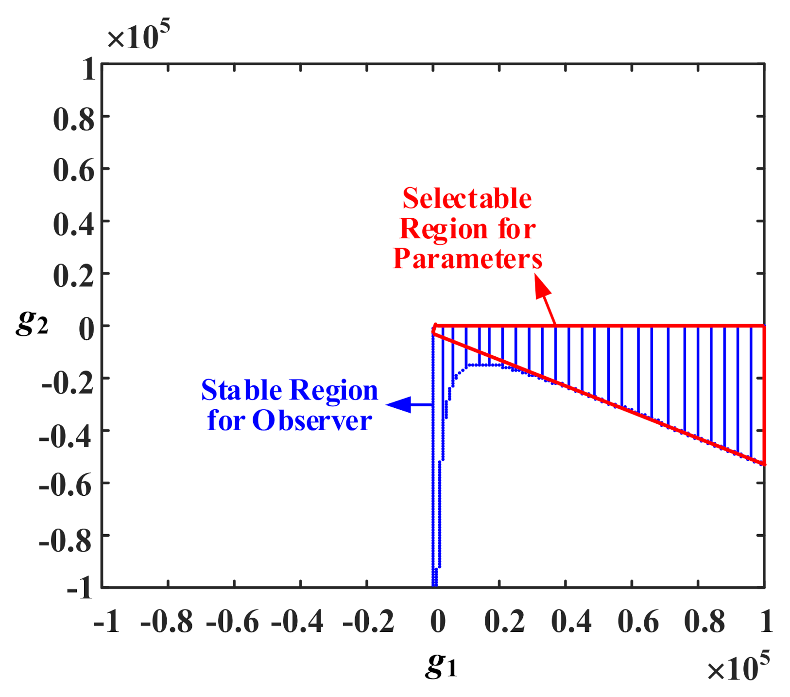
Figure 8. Finally, the stable region of
g1 and
g2 applicable to the specified LCL parameters listed in
Table 1 is shown in
Figure 9. We can deduce that
g2 should be negative and should not be too large. When
g1 increases, the optional range of
g2 also become wider.
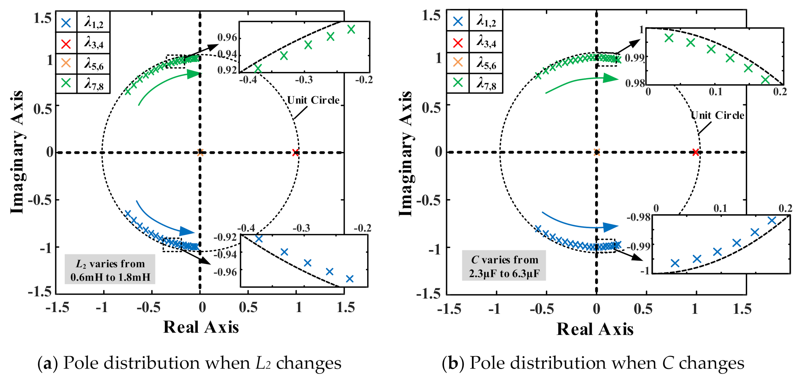
Although the feedback matrix can be decided through the above-mentioned parameter scanning method, some abnormal situations might challenge the stability of DOB. For example, the grid-side inductor
L2 changes under the influence of the grid impedance
Lg and its accurate value is hard to be determined. Moreover, the actual parameters of filter capacitors usually fluctuate after a long-time operation. Therefore, the robustness of DOB while the parameters of LCL filter are changing should also be examined.
Figure 10 shows the varying trend of the pole distribution when different main circuit parameters are substituted in order to confirm the adaptability and robustness of DOB. According to
Figure 10, we can see that the changes in
L2 and
C have similar effects on the pole positions of the DOB. The poles close to the origin and the real axis are not significantly affected. However, the conjugate poles in the left half plane gradually move to the right side when
L2 and
C increase. The pole positions during this change all keep inside the unit circle. Therefore, the DOB maintains its ability in such circumstances. Thus, its robustness can be guaranteed.
4. Simulation and Experimental Results
For purpose of verifying the control effect and feasibility of the algorithm presented in this paper after adding AD to the LCL filter based on DOB. The simulation model is built up in Matlab/Simulink by realizing the diagram shown in
Figure 1. The system parameters are given in
Table 1. The value of virtual resistor is set to 50 Ω.
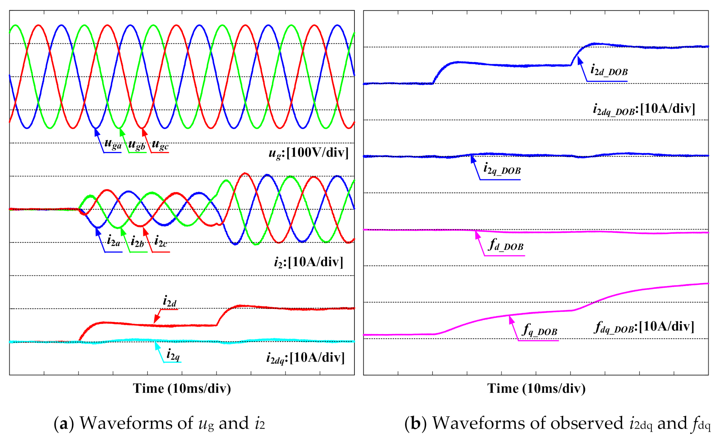
To evaluate the steady state and dynamic performance of the PCS with the presented control algorithm, the start-up process of PCS for discharging operation is tested first. The reference d-axis current
i2dref is directly set to 5 A at 20 ms. Then, at 60 ms,
i2dref is set to 10 A. Meanwhile,
i2qref is kept as 0 A for unity power factor operation during this process. The simulation results are shown in
Figure 11a. It can be seen that the grid-injected current is of good quality and can track the reference value accurately. At the same time, waveforms of disturbances estimated by the DOB are shown in
Figure 11b, which include both the internal coupling items and external disturbances of the PCS. Therefore, DOB is able to estimate the unmeasurable disturbances that need to be compensated in different conditions as an enhancement for anti-interference ability of the overall system. The similar simulation results are given in
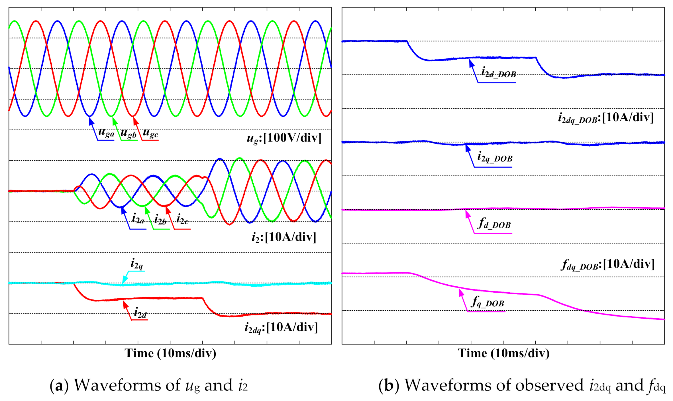
Figure 12 to verify the feasibility of control method for charging condition.
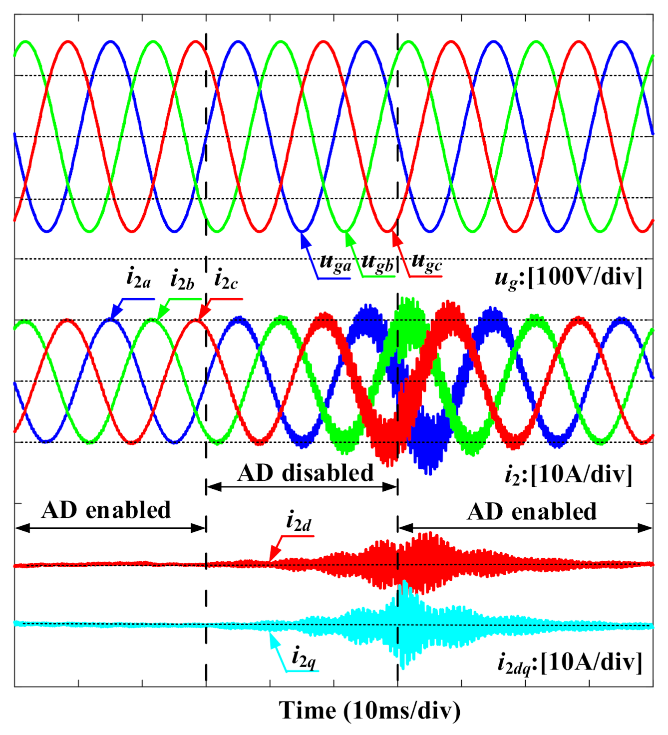
In order to confirm the effectiveness of the AD strategy for the LCL filter based PCS, a comparison study is carried out by invalidating the second derivative of grid-side current for a short time. The obtained simulated grid voltage and current waveforms are shown in
Figure 13. AD is shut down within the time range from 30 ms to 60 ms. After AD is disabled, it can be seen that severe current oscillation emerges immediately until AD is enabled again at 60 ms. According to the simulation results, we can deduce that the control method only relying on PI controller is not enough to suppress the resonance of LCL filter. However, this issue is effectively solved by adopting the second derivative of grid-side current feedback branch in the control loop.
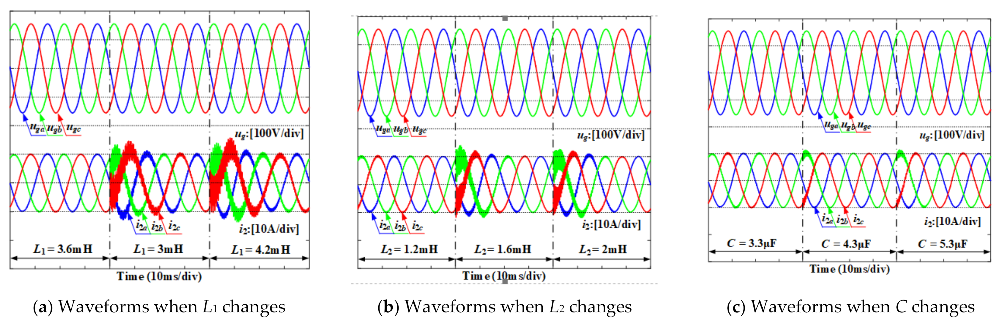
In addition, the robustness of presented control method is tested too. In order to imitate the influence of main circuit parameter drift in practice,
L1,
L2 and
C are deliberately set to different values with reasonable errors in the vicinity of their rated values given in
Table 1, respectively. The simulation results are shown in
Figure 14.
Figure 14a–c depict the waveforms when parameters
L1,
L2 and
C are not accurate, respectively. We can see that the negative impact of parameter drift exists but is not significant enough to cause stability problems.
In order to further confirm the feasibility of the presented control method, a downscaled experimental prototype consists of dSpace and Danfoss inverter FC302 is built up. The parameters of the prototype are the same as those used in the simulation model as given in
Table 1. The voltage signals are acquired by probe GWinstek GDP-025 (Suzhou, China). The current signals are acquired by probe HIOKI 3276 (Nagano, Japan). Meanwhile, the oscilloscope DL1640 manufactured by Yokogawa (Tokyo, Japan) is used to capture the waveforms.
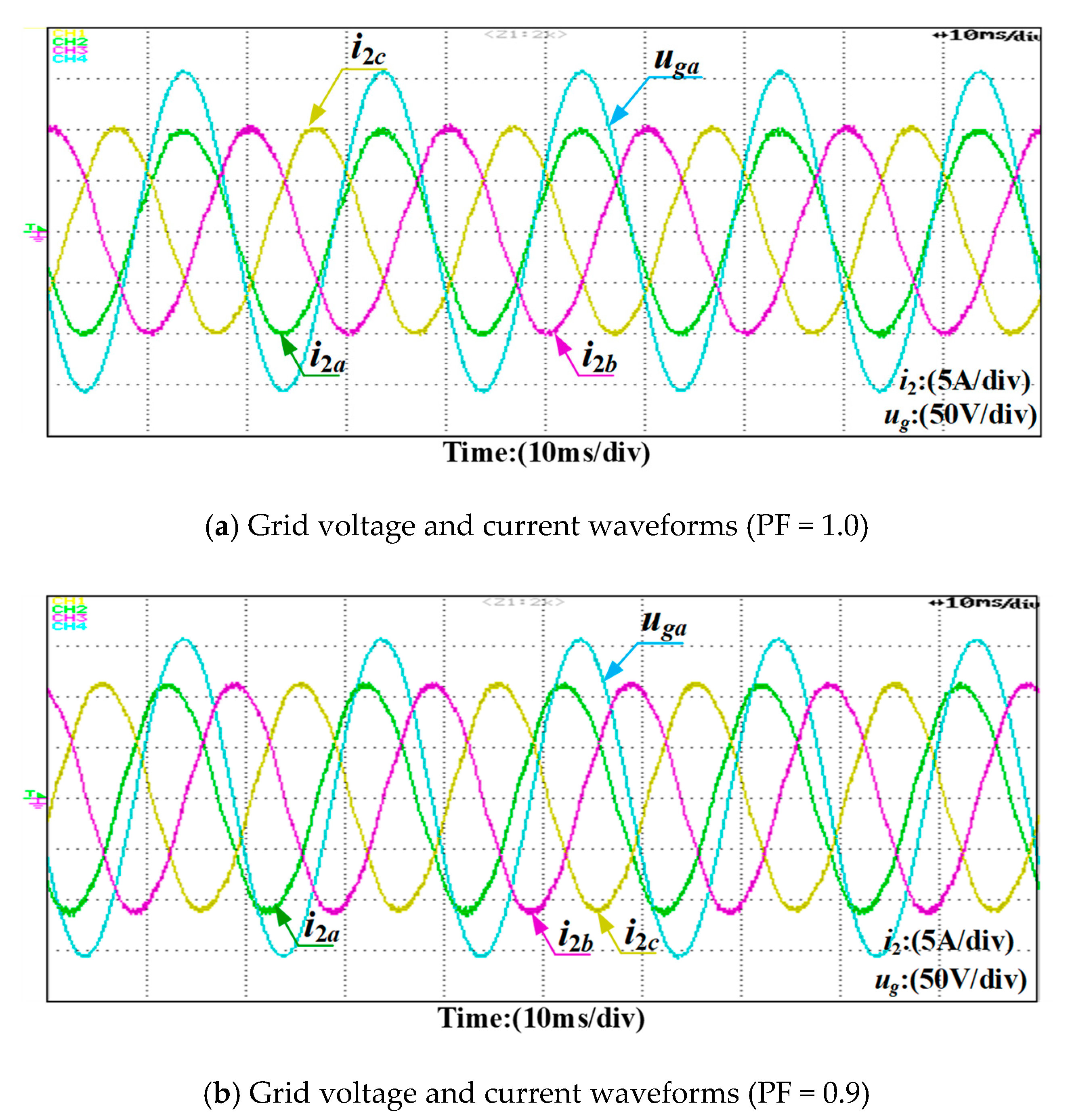
Normal discharging operation with unity power factor is tested first. Grid voltage and current waveforms obtained from the prototype are shown in
Figure 15. According to
Figure 15a, we can see that unity power discharging operation is guaranteed since
uga and
i2a always keep in phase. Grid-injected currents are all sinusoidal, which meets general power quality requirements. By setting
iqref to 5 A, reactive power can also be generated as shown in
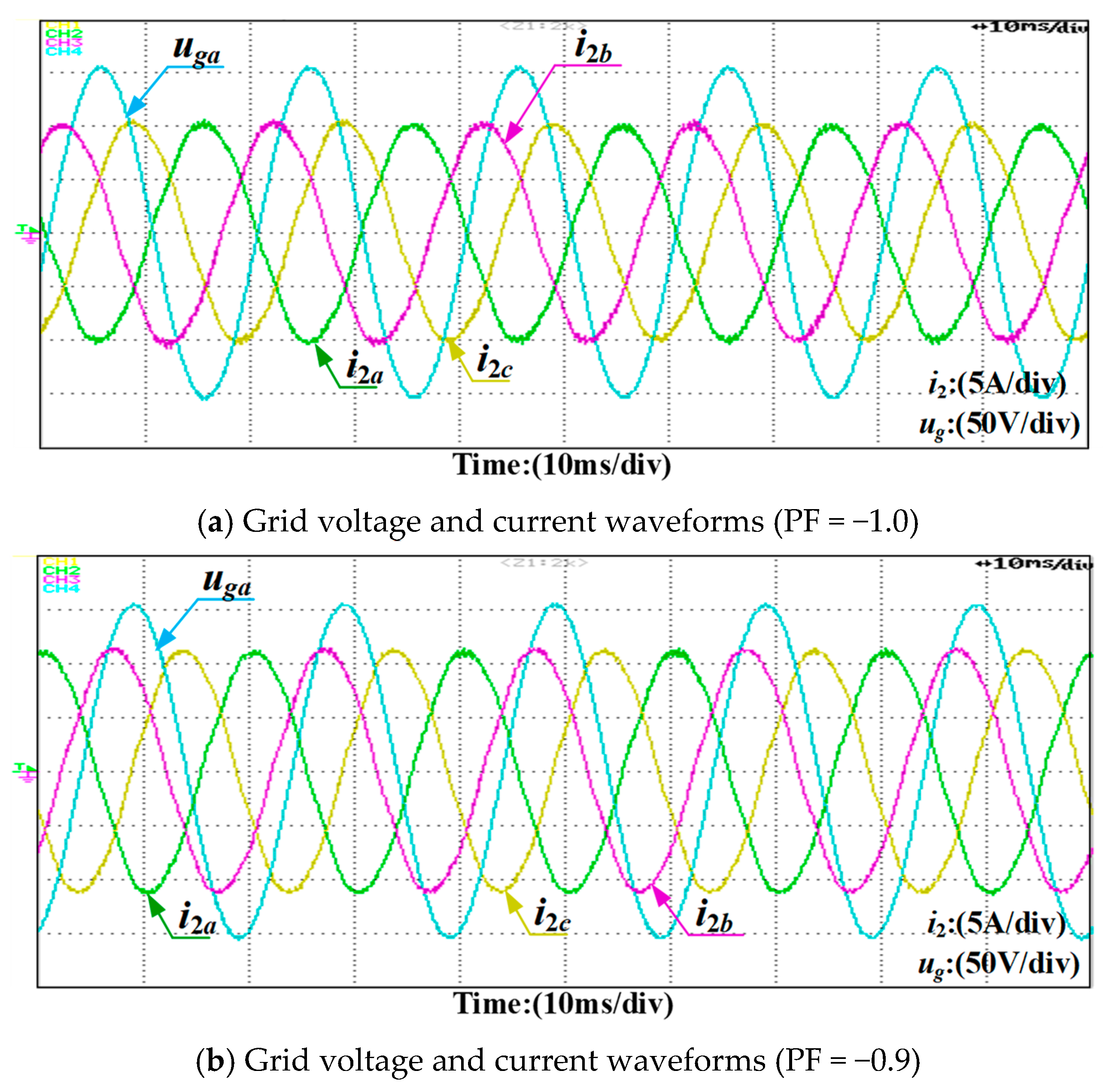
Figure 15b. In this situation, the current lags behind the grid voltage by approximately 25 degrees, which indicates reactive power is produced by the PCS. This function can be further used to achieve partial replacement of static Var compensator. Similar tests for charging operation are also carried out. The experimental results are shown in
Figure 16. As a brief summarization, the steady state performance of PCS based on DOB can be verified.
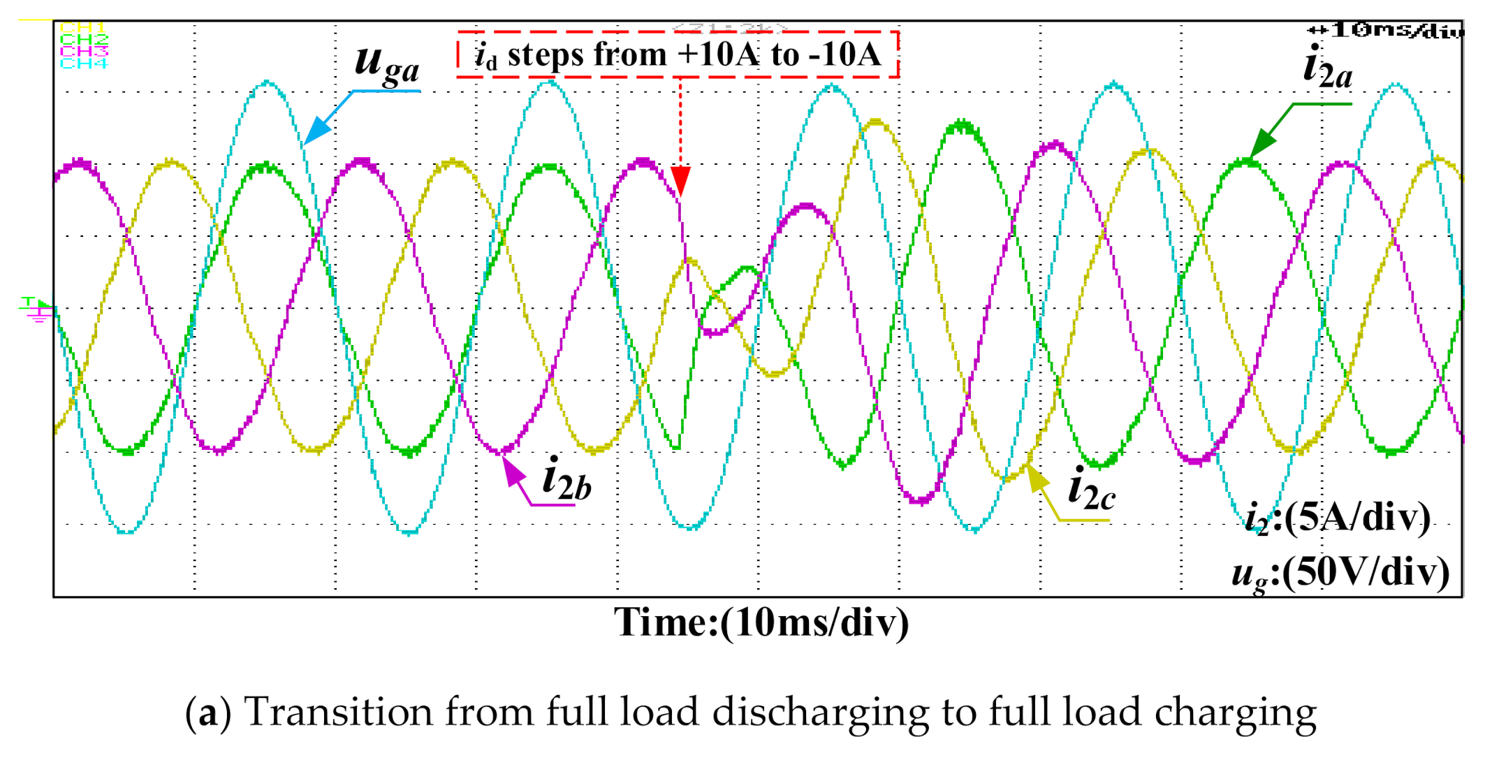
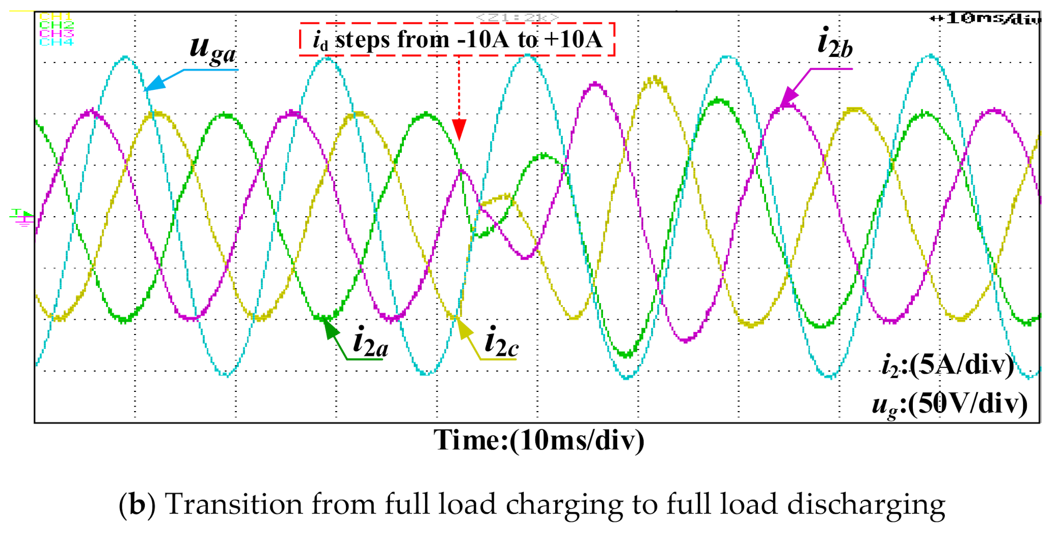
Furthermore, the transient response feature of PCS is tested. The experimental results obtained from the PCS prototype are illustrated in
Figure 17. At first,
i2dref is set to 10 A. Then, it steps down to −10 A suddenly to reverse the flow direction of electric power. Based on this condition, representative test result for transition from full load discharging state to charging states is yielded as shown in
Figure 17a. We can see that the full load transient process terminates within 10 ms, which meets most requirement in industrial applications. Meanwhile, the symmetrical transition from charging to discharging is also tested.
Figure 17b shows the experimental results. The dynamic performance of PCS can be verified.


