Abstract
Low level modular multilevel converter (MMC) is a promising candidate for medium voltage applications such as MVDC (medium voltage DC current) transmission and megawatt machine drives. Unlike high-level MMC using nearest level modulation (NLM), the low-level MMC using the pulse width modulation (PWM) or NLM + PWM is affected by a common mode voltage (CMV) due to a frequent change of a switching state. This CMV causes electromagnetic interference (EMI) noise, common mode current (CMC) and bearing current leading to a reduction in the efficiency and durability of the motor drive system. Therefore, this paper provides a mathematical analysis on how the switching state affects the CMV and proposes three software based CMV reduction algorithms for the low level MMC system. To reflect the characteristic of MMC modulation strategy for upper and lower reference voltage independently, two separate space vectors are used. Based on the analysis, three different CMV reduction algorithms (complete CMV reduction (CCR), DPWM CMV reduction (DCR) and partial CMV reduction (PCR)) are proposed using NLC + PWM modulation strategy. The performance of the proposed CMV reduction algorithms was verified by both simulation and experimental result.
1. Introduction
Modular multilevel converter (MMC) is an attractive and advanced multilevel converter topology in the electric power industry. Due to its modularity and scalability, the MMC can extend the active voltage level to meet the requirement needed in some industrial applications such as VSC-HVDC (voltage sourced converter high voltage direct current), FACTS (flexible alternative current transmission system), MVDC (medium voltage direct current) and variable-speed drive systems [1,2,3,4,5,6,7,8,9,10,11]. Compared with 2-level or other multilevel topologies, the MMC also has the lower harmonic content of an output waveform, the higher voltage operating capability, reduced voltage derivatives, the smaller output filters and an ability for redundant operation and fault-tolerant control [9,10,11]. In the power industry area, the MMC is usually divided into two categories: the high level MMC and the low level MMC. The high level MMC, namely the hundreds of the voltage level, is used in the high voltage applications. Additionally, the low level MMC, the dozens of the voltage level, is for the medium voltage applications.
Since MMC is configured of series-connected submodules (SMs) including power semiconductor devices, it still has a common mode voltage (CMV) issue especially in the medium voltage applications. In case of the high voltage applications, which adopts a nearest level modulation (NLM) method, the problem of the CMV is not a serious challenge. The NLM is one of staircase modulation methods, which decides the switching states of SM with duty cycle as 1 or 0 every control period without any carrier signals. It is very simple to implement and synthesize SM capacitor voltages [12,13,14]. However, the MMC in medium voltage applications do not use the NLM method due to the performance degradation in the output waveform. Instead, they use a pulse width modulation (PWM) method. There are several representative PWM methods for MMC: phase shifted (PS), phase disposition (PD), phase opposition disposition (POD) and alternative phase opposition disposition (APOD) [15,16,17,18,19,20,21]. Among these PWM techniques, as the PD-PWM method generates 2N + 1 voltage level (where N is the number of SMs in an arm) and uses the optimized switching sequence on a hexagon for three phases system, it has the best performance on total harmonic distortion (THD) [22,23]. Additionally, a hybrid modulation technique, NLM + PWM, also exists [23]. The principle of the NLM + PWM method is that only one carrier crossing the reference generates the gating signals with 0~1 duty ratio like the PWM method and the other gating signals are generated through the NLM method. It is similar to the PD PWM method and, in terms of the implementation, the only difference between them is that PD PWM uses the multicarrier and NLM + PWM uses one carrier. The NLM + PWM method can also be implemented through a space vector [23]. However, as these modulation techniques make a frequent change of switching states, the CMV becomes an undesirable and critical issue in the medium voltage applications.
The CMV is commonly defined as a voltage difference between a DC side neutral point and a load side neutral point in the DC–AC power conversion system [24]. As the pole voltages synthesized by the switching operation of each phase are discontinuous, the common mode voltage has high frequency components, which leads the stray impedance existing between two points to be decreased. The problems of the CMV are: (a) an electromagnetic interference (EMI) noise, (b) a common mode current (CMC) damaging physical systems and causing malfunctions of devices related to networks or protections and (c) a bearing current reducing the durability and efficiency of the motor drive systems [25,26,27,28,29]. Although the DC voltage of the MMC is distributed into the capacitor of SMs, if the MMC has the low number of SMs, the magnitude of the CMV is relatively high enough to have a serious effect on the whole system [30].
In order to reduce the CMV generated in the MMC, various reduction methods have been studied [30,31,32,33]. The paper in [31] deals with the CMV reduction for the flying-capacitor modular multilevel converter based motor drive system. Although this algorithm successfully eliminates the CMV, it causes a 10% increase in the switching frequency, which will lead to a higher switching loss. The paper in [30] adopts the same CMV reduction algorithm used in [31] and applies to the MMC system connected with an unsymmetrical grid. Another CMV elimination scheme has been proposed for an open-end stator winding induction motor [32]. An open-end stator winding induction motor requires the dual MMC system and the interaction between the CMV of MMC1 and MMC2 is manipulated to cancel the overall CMV current in to the machine.
This paper proposes a CMV reduction algorithm to a half-bridge (HB) three-phase MMC system that is configured as double star chopper-cells (DSCCs) of [33,34]. First, the CMV is mathematically analyzed to determine how the interaction of the switching sequence in the upper and lower arm of the MMC system affect the magnitude of the CMV. Then, the switching sequence and the resulting CMV for various modulation methods are explained using a separate space vector diagram to the upper and lower arm of the MMC system. Based on the analysis, three different CMV reduction algorithms (complete CMV reduction (CCR), DPWM CMV reduction (DCR) and partial CMV reduction (PCR)) are proposed. The three CMV reduction algorithms provide different results with respect to the CMV and the harmonic content of the output current and hence applied based on the specific applications. The rest of the paper is organized as follows. In Section 2, the principle of the three-phase N + 1 level MMC is described. Section 3 covers the mathematical analysis of the CMV. In Section 4, the proposed algorithms for the CMV reduction are elaborated. Section 5 and Section 6 provide the simulation and experimental results, which verify the performance of the proposed algorithms, respectively. Finally, Section 7 states the conclusion.
2. Basics of MMC
Figure 1 shows the three-phase N + 1 level HB-MMC. It consists of a DC source, an arm inductor and six-arms where each arm has N series-connected SMs. The half-bridge submodule (HBSM) is comprised of a capacitor and two power semiconductors. During the normal operation, based on a switching state of the SM and a direction of an arm current flowing through the arm, the SM capacitor () is charged or discharged. Normally, the two switches, an upper (S1) and a lower (S2) switch, operate complementally. The definition of a switching function for the SM is described as [35]:
where the subscript, x, denotes a phase among a, b, and c and the subscripts, u and l, are denoted for the upper and the lower arm and the subscript, n, represents the SM number (1, 2, …, N). Table 1 shows the operation of the SM. For example, if the switching function, , is 1 and the positive arm current flows through the SM, the SM capacitor voltage is charged. Assuming the voltage drop across the SM components to be negligible, the SM voltage is defined as (2) [35].
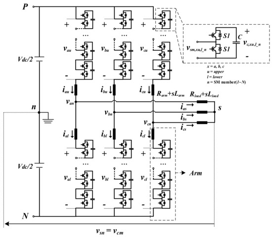
Figure 1.
Three-phase N + 1 level modular multilevel converter (MMC) circuit configuration.

Table 1.
Submodules (SM) capacitor voltage state based on the switching states and the direction arm current.
The resulting arm voltages of the MMC are synthesized from SM voltages based on the corresponding switching states, as deduced in (3).
Figure 2 shows the single-phase equivalent circuit of the three-phase MMC. The currents, and are the upper and lower arm current, respectively. The output phase current and the leg current are calculated form the arm currents, as described in (4) and (5). From (4) and (5), the arm currents can be deduced as (6) and (7) [5].
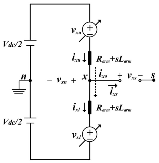
Figure 2.
Single-phase equivalent circuit of three-phase N + 1 level MMC.
From the closed loops of the single-phase equivalent circuit, the voltage equations can be induced as [5]:
where the lower character, s, is the differential operator, . From (8) and (9), the output electromotive force (EMF) and the leg internal voltage can be defined as (10) and (11), respectively.
Substituting (4) and (10) into (8), the pole voltage is written as (12). Additionally, substituting (5) and (11) into (9), the leg internal voltage is deduced as (13) [5].
The upper and lower arm voltage synthesizes reference voltages to regulate the output current and leg current. The control for the MMC adopts a direct modulation method [36]. The output current is regulated by a vector control based on a fundamental frequency rotating frame. In case of the leg current, since the direct modulation method assumes that the arm voltage is constant without considering capacitor voltage variation, a negative sequence 2-nd harmonic current flows through the inner side of the MMC. So, the negative sequence current controller, called CCSC, is proposed in [36]. From (12) and (13), the upper and lower arm reference voltages are deduced as [36]:
where an asterisk, “*”, represents a reference. The entire control algorithm for the direct modulation method is shown in Figure 3.
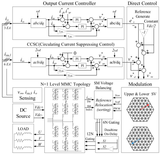
Figure 3.
Direct modulation method of three-phase MMC.
3. Analysis of CMV in Three Phases N + 1 Level MMC
3.1. Definition of CMV
The capacitor voltages of the SM should be balanced for the normal operation of the MMC. Since the DC bus voltage is evenly distributed to the SM capacitors, each capacitor can be approximated to . From (2), the SM voltage is rewritten as (16).
Substituting (3) and (16) into (8) and considering that the resistance of the arm inductor is small, the pole voltage can be deduced as (17) [24].
The CMV is defined as the average of the three pole voltages, as described in (18). From (17) and (18), the CMV for the MMC is deduced as (19).
The sum of the switching function in (19) represents the turn-on number of the SMs for the upper or lower arm and is expressed as (20).
Additionally, assuming a balanced three phase system, the last term of the right-hand side of (19) can be canceled. Substituting (20) into (19), the definition of the CMV is rewritten as (21).
The difference between the turn-on number of the upper and lower SMs is defined as the common mode voltage step, , in (22).
Substituting (22) into (21), the CMV for the three phases MMC is simplified as (23).
From (22) and (23), it can be concluded that the CMV of the MMC is an integer multiple of and can be used to regulate the CMV in the MMC.
3.2. CMV Anlaysis on Space Vector
The DC bus voltage of the MMC is synthesized by the SM capacitor voltages. To keep the DC bus voltage constant, the inserted SMs in one phase should be kept as N. However, as shown in (14) and (15), since the reference voltages of the upper and lower arm include the leg internal reference voltage, the sum of them is not . Additionally, in the low level MMC using the PWM or NLM + PWM method, the switching sequence varies depending on the phase difference between the carriers. Theses result in the CMV generation in the MMC. Therefore, in order to analyze the CMV and , two independent space vectors were used for the upper and lower arm references.
Figure 4 shows that the three-phase 5-level MMC. In Figure 4a, it shows that the upper and lower reference voltage vectors ( and ) were located on a separate space vector, and , respectively. On the space vector, the two reference voltage vectors are defined as:
where and [23]. Substituting (14), (15), (16) and (17) into (24), the reference voltage vectors can be deduced as:
where , and are the turn-on number of three-phase upper and lower SM. In Figure 4b, the turn-on number of SMs represents the switching sequences on the space vector. Therefore, the NLM + PWM method can be analyzed on the hexagons. As shown in Figure 4b, the center of the outer hexagon (), , is changed to the point, , where the active voltage vector () is located. Additionally, the 2-level space vector () is configured around the reference voltage vector. The reference voltage vector is expressed as:
where is the active voltage vector defined as the base reference voltage vector for the NLM method and is the PWM reference voltage vector for the PWM method. Both and can be calculated from (24), but these can also be simply implemented by the following calculations:
where is the base sequence (BS), which means the number of submodules that must be kept ON over one switching period, is the PWM reference voltage and is the output voltage of the submodule, assumed as . Since the base sequence () is the result of the floor function, it always has the integer value and is used for the NLM method. The PWM reference voltage () is used for the PWM method.
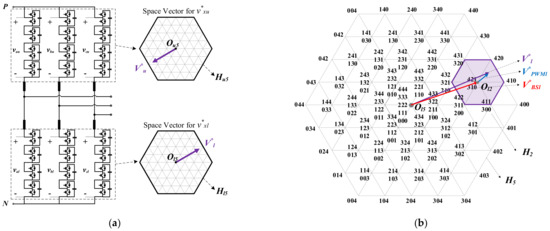
Figure 4.
Space vector and nearest level modulation (NLM) + pulse width modulation (PWM) analysis for the common mode voltage (CMV) in the three-phase 5-level MMC: (a) independent space vector for the upper and lower arm reference voltages and (b) NLM + PWM analysis for the reference voltage vector on the space vector.
Figure 5 shows the modulation process for the lower arm reference, using the NLM + PWM method on the space vector and the switching sequence of the three-phase 5-level MMC. First, the base sequence, is determined by (27). Accordingly, Figure 6a shows that the always-on number of the submodules for phase a, b and c of the lower arm were decided to be 3, 1 and 0, respectively. Additionally, then the two-level space vector is formed around and the PWM reference voltages are modulated with a carrier. With the down-up carrier starting from off-sequence to on-sequence, the number of on-state SMs, , is 0→1→2→3→3→2→1→0 in sequence. As the sum of BS of the lower arm, , is 4, the total number of the on-state SMs, , is 4→5→6→7→7→6→5→4 in sequence. The process for the upper arm can also be carried out in the same way. The modulation results for the upper and lower arm are depicted in Figure 6b. If both upper and lower arm NLM + PWM schemes use the same carrier, the CMV happen occurs 12 times for .
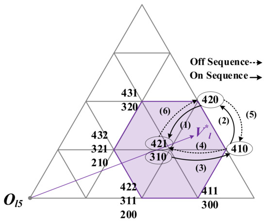
Figure 5.
Implementation of NLM + PWM for the lower arm reference voltage vector: the movement of switching sequence for .
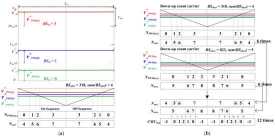
Figure 6.
Implementation of NLM + PWM for the both arm reference voltage vector: (a) determination of the BS and the PWM reference voltage of and (b) switching sequences for both arms references and the CMV generation.
The PS, POD and APOD modulation methods had different results in the CMV generation. Since the NLM + PWM or PD methods had in-phase carriers for the two arms, the switching patterns were out of phase as depicted in Figure 7a. However, in Figure 7b, the PS, POD and APOD methods had carriers with 180-degree out of phase, both switching patterns were in phase each other. Table 2 summarizes the characteristics of the switching pattern, the CMV voltage and the output voltage for various carrier-based modulation methods. Among the carrier-based modulation methods, the NLM + PWM had the highest voltage level, which means the best performance of the output waveform. Therefore, based on the NLC + PWM method, the reduction strategies for the CMV were discussed in the following sections.
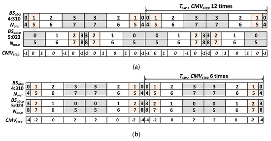
Figure 7.
Switching patterns and CMV generation with different carriers. (a) In-phase carriers (switching pattern is shifted) and (b) 180° out-of-phase carriers (switching patter is in phase).
Table 2.
Characteristics of the CMV and the output waveform for various carrier-based modulations.
4. CMV Reduction in MMC
4.1. Complete CMV Reduction (CCR) Method
The complete CMV reduction (CCR) method selectively uses switching sequences that can bring the common mode voltage to null [37]. The NLC + PWM technique modulates the reference voltage by using the three active vectors nearest to the reference voltage vector, which results in a good THD characteristic. However, it causes the CMV in most switching sequences. Assuming that both arm references are 180° out-of-phase in the three phases N + 1 level MMC topology, it can be found that the CMV does not happen under the condition, defined as (29).
The switching sequences satisfying (29) make a new 30-degree out-of-phase N − l level hexagon. For example, as shown in Figure 8a, in the 5-level MMC, the switching sequences of which the arithmetic operation in (29) is 6 configures the 30-degree out-of-phase 3-level hexagon, . The conventional NLM + PWM technique for both upper and lower arm references voltage vector ( and ) uses the switching sequences, (023), (034), (024) and (134), nearest to with the BS (023) and (421), (420), (410) and (310), nearest to with the BS (421), respectively. From (22) and (23), the CMVs are generated in the most cases. However, in the CCR method, the BS for the upper arm is changed to (023) with the switching sequences, (123), (033) and (024) while the BS for lower arm is changed to (321) with switching sequence (321), (411) and (420). Therefore, from (21) and (22), the CMV does not exist in CCR method.
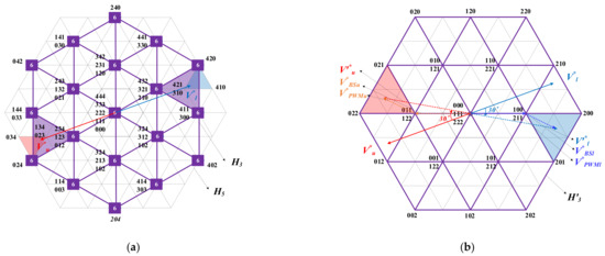
Figure 8.
The complete CMV reduction (CCR) method in the 5-level MMC: (a) 30-degree out-of-phase space vector and the switching sequences for the cancellation of the CMV and (b) the manipulation of space vector and references for implementation of the CCR method.
The implementation of the CCR method requires two steps: modulation for the references in N − l level space vector and reconstruction for the N − l level-based switching sequences to N + 1 levels-based switching sequences. The modulation process is similar to the conventional one, but, in order to modulate the references N − l level space vector of which the phase is shifted anticlockwise by 30-degrees and the magnitude is times smaller than N + 1 level space vector, the references and the space vector should be rotated to the position of N + 1 level space vector. The N − l level space vector is rotated clockwise by 30-degrees and the magnitude is scaled to N + 1 level space vector. With the change in the N − l level space vector, the references for each arm are shifted by 30-degrees, expressed in (30)–(32).
Additionally, the new base and PWM reference voltage vectors are induced as (33) and (34).
From (27) and (28), the new base sequence and PWM reference voltages are calculated as (35) and (36).
As show in Figure 8b, the reference voltage vectors and 3-level space vector scaled by () were rotated by 30-degrees. Additionally, the switching sequences were redefined on the 3-level space vector (). The base and PWM reference voltage vectors ( and ) also moved with the 3-level space vector. Therefore, the upper arm switching sequences were (011), (021) and (022) with the upper arm base sequence of (011) and the lower arm switching sequences were (100), (200) and (201) with base sequence (100).
The reconstruction of the BS () were implemented to determine the number of the turn-on SMs for the N + 1 level MMC. Then substituting (25) and (29) into (33), the reconstructed turn-on SMs for each arm were deduced as (37)–(39).
The PWM reconstruction, however, requires a simple calculation due to the switching operation of a PWM module in a hardware system. Therefore, the reconstruction factor is defined as (40)–(42).
Additionally, then, the reconstructed switching signals were directly determined by logical operations defined as:
where and are the reconstructed and manipulated switching function, respectively, the operator (), is the exclusive OR (XOR). If the reconstruction factor is 1 from (40) to (42), the result of the switching function is added to the reconstructed BS. If the reconstruction factor is 0, the result is subtracted from the reconstructed BS. Figure 9 shows that the CCR method determined the upper and lower arms switching patterns with the reference voltage vectors in Figure 8 and the six turn-on SMs satisfying (29) were generated. Therefore, the CMV was canceled over one switching period.
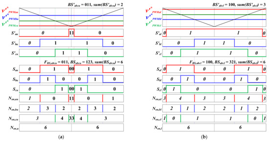
Figure 9.
The switching patterns and the turn-on SM for the upper and lower arms using the CCR method: (a) upper arm the switching pattern and the number of turn-on SMs and (b) lower arm the switching pattern and the number of turn-on SMs.
4.2. DPWM CMV Reduction (DCR) Method
The DPWM CMV reduction (DCR) method uses the principle of the discontinuous PWM (DPWM) technique. In this paper, 60-degree DPWM was adopted to reduce the CMV. As shown in Figure 4b, it can be found that a few switching sequences could generate the same active voltage vector. For example, in Figure 5 and Figure 6b, the switching sequences, (421), (420), (410) and (310) were used to modulate the lower arm reference voltage vector () and the switching sequences, (421) and (310), generated the same active voltage vector. If the switching sequences for one active voltage vector are limited to only one switching sequence by injecting an offset voltage, the number of the CMV generation can be reduced.
The maximum and minimum PWM reference voltages are defined as:
where max() and min() select the maximum and the minimum out of variables, respectively. The offset voltage for 60-degree DPWM is defined as:
where and are the maximum and the minimum of three-phase PWM reference voltages for the upper and lower arms, respectively. Adding (45) to both (14) and (15), the upper and lower arm references for the DCR method are deduced as (47) and (48):
In Figure 10a, without the DCR method, the CMV happened 12-times during a switching period. Additionally, it shows that the switching sequences, (310) and (421), generated the same active vector and the number of the turn-on SMs were 4 and 7, respectively. However, after applying the DCR method, the offset voltages ( were added to each PWM reference voltages and caused the reduced switching patterns. Additionally, the switching sequence (321) was not used, but the switching sequence (421) was extended by the switching time of the (321) switching sequence. Since the number of the active voltages were reduced, the CMV occurred 8-times with about a 33% decrease.
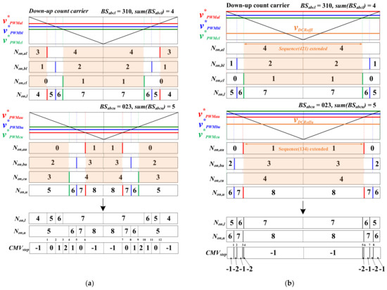
Figure 10.
Implementation of the CCR method: (a) the switching patterns and the CMV before applying the CCR method and (b) the switching patterns and the CMV after applying the CCR method.
4.3. Partial CMV Reduction (PCR) Method
The normal NLC + PWM technique always causes five , −2, −1, 0, +1 and +2. As shown in Figure 11a, if the reference voltage vector rotates on the space vector over one reference period (60 Hz, 16.67 ms), the 2 happens every 60-degrees. If the difference between the sum of the base sequences of the upper and lower arm reference voltages in Figure 11b was , the was 2 as shown in Figure 11a. To reduce the maximum CMV and limit to −1, 0 and +1, the partial CMV reduction (PCR) method evaluated the conditions generating the maximum and then injected the maximum CMV as the offset voltage to the reference voltages.
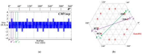
Figure 11.
Generation of the CMV of two reference voltage vectors ( and ) in the normal NLM + PWM method: (a) +2 and −2 CMV step generation over one reference period and (b) distribution of sum of BS of two vectors ( and ) on the space vector.
Figure 12 shows the switching pattern for the reference voltage vectors ( and ) of Figure 11. In Figure 12a, the BSs of two arms were (310) and (023) and their sum were 4 and 5, respectively, which resulted in the difference of −1. The maximum of the CMV voltage occurred at the point where the maximum of the lower arm turn-on SM () and the minimum of the upper arm turn-on SM () occurred. Since the two switching sequences, (310) and (023) output the active vector of same magnitude and opposite direction, the offset voltages were added to each arm to remove the maximum the CMV. The condition for evaluating the maximum CMV is defined as (49).
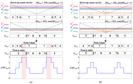
Figure 12.
The maximum CMV generation with and without the PCR method: (a) +2 CMV generation without the PCR method and (b) decreased the maximum of the CMV with the PCR method.
According to (49), the offset voltages for the PCR method are defined as (50) and (51).
As shown Figure 12b, the offset voltages were added to the reference voltages. Since the maximum and the minimum of the number of the turn-on SMs did not occur at the same time, 2- was removed. The decrease of was proportional to the number of the section where the CMV generates. This means that the CMV reduction was not even according to a fundamental frequency and a modulation index (MI). Generally, the PCR method resulted in about a 10–15% CMV reduction.
5. Simulation
The 5-level MMC was used to verify the proposed algorithms in MATLAB/SIMULINK. The parameters for the MMC system were designed based on the circulating current, the MMC level and the magnitude of the DC link voltage [38]. The switching frequency were determined by a DSP calculation time of a laboratory setup including the AC output control, the circulating current control and the voltage balancing algorithm. The parameters of the system are summarized in Table 3. The magnitude and quantity of the CMV voltage were investigated with and without the proposed algorithms. It was also investigated whether the proposed algorithms have an effect on the output waveform.
Table 3.
Simulation Parameters for the 5-level MMC system.
Figure 13 shows the results of the NLC + PWM method without any proposed algorithms. The modulation index was 0.8. In Figure 13a,b, the maximum of was 2 and, from (22) and (23), the CMV was proportional to the . The CMV occurred 20,000 times during one reference period and each step of the CMV was 150/24 = 6.25 V. Since NLC + PWM had good performance due to the 2N + 1 level output voltage, the THD of output waveform was 0.57%.
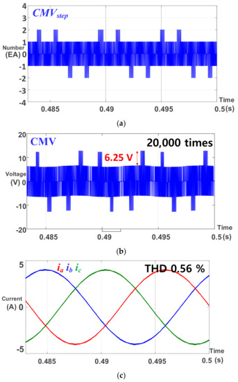
Figure 13.
Simulation results without the proposed algorithms: (a) ; (b) CMV output and (c) three-phase output currents and total harmonic distortion (THD).
Figure 14, Figure 15 and Figure 16 shows the results for the three proposed algorithms. Figure 14 shows the CCR algorithm results. Since the CCR method used specific sequences satisfying (29), the CMV was removed completely. However, as the active voltage vectors were not nearest to the reference voltage vector, the output waveform had a higher THD (1.23%). The DCR method, as shown in Figure 15, reduced the CMV by 33% compared with the result without the proposed algorithms in Figure 13. Additionally, it does not have a serious effect on the THD result (0.57%). In Figure 16, the PCR method removed the maximum CMV using the offset voltage. Similar to the DCRM result, the PCR method also did not cause a critical problem on the output currents (THD 0.58%).
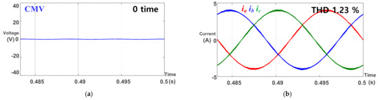
Figure 14.
Simulation results for the CCR method: (a) CMV output; (b) Three-phase output currents and THD.
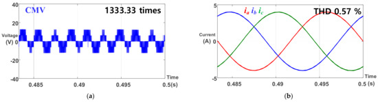
Figure 15.
Simulation results for the DPWM CMV reduction (DCR) method: (a) CMV output and (b) three-phase output currents and THD.
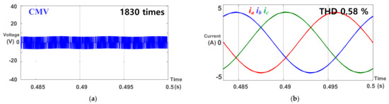
Figure 16.
Simulation results for the partial CMV reduction (PCR) method: (a) CMV output and (b) three-phase output currents and THD.
6. Experiment
The proposed CMV reduction methods were verified by experiment performed on a 5-level MMC setup as shown in Figure 17. The specifications of the system were the same with that of the simulation given in Table 3. Additionally, the dead-time of power switch operation was 1 us. The 5-level MMC laboratory setup was implemented by the DSP (TMS320C28346) for main controller and the FPGA (CYCLONE4) for PWM modules.
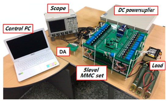
Figure 17.
The 5-level MMC experiment setup.
Figure 18 shows the test results without the proposed algorithms using the NLC + PWM and MI = 0.8. The CMV occurred 12-times for one switching period. From (23), the CMV was 150/24 = 6.25 V per step with the maximum was 2 steps. The enlarged waveforms, shown in Figure 18b, had the voltage ripples when the CMV voltage was changed. It was mainly caused by the dead time to prevent short circuit. Figure 19 shows the waveforms with the CCR method. The CCR method removed the CMV, which was generated by the switching operation of the SMs. However, the CMV still exited due to the deadtime effects. In Figure 20, the DCR method only reduced the number of the CMV generation and the CMV occurred 8-times during a switching period. In Figure 21, the PCR method removed the maximum CMV and the was limited to 1.
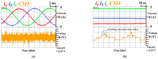
Figure 18.
Experiment results without the proposed algorithms: (a) three-phase output currents and CMV output and (b) enlarged waveforms of (a).
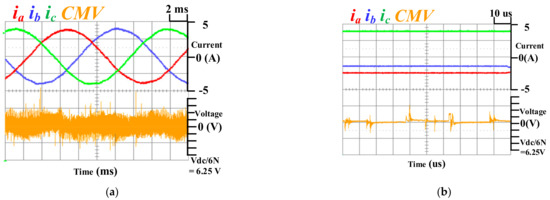
Figure 19.
Experiment results for the CCR method: (a) three-phase output currents and CMV output and (b) enlarged waveforms of (a).
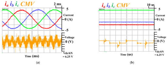
Figure 20.
Experiment results for the DCR method: (a) three-phase output currents and CMV output and (b) enlarged waveforms of (a).
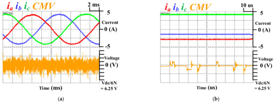
Figure 21.
Experiment results for the PCR method: (a) three-phase output currents and CMV output and (b) enlarged waveforms of (a).
7. Conclusions
In this paper, the common mode voltage analysis based on two separate space vectors was proposed. The two separate space vectors could represent the turn-on SMs as the switching sequence for three-phase arms and the CMV was analyzed in detail. Additionally, three common mode voltage reduction methods were proposed: (a) CCR method, (b) DCR method and (c) PCR method. The CCR method removed the CMV voltage completely, but it caused higher distortion of the output current compared with other proposed algorithms. The DCR method used the 60-degree DPWM method and reduced the CMV by about 33%. However, the maximum CMV kept 2 which was the result without the proposed algorithm. The PCR method always limited the maximum value of the CMV to . Since the maximum CMV was 2 in the NLC + PWM method, the PCR algorithm could remove 2 . However, the fluctuation of the CMV was reduced by 8%. In both the DCR and PCR method, the third harmonic component is the offset voltage, which reduced the CMV and had almost no effect on the output current. As a result, the THD was 0.56% without the proposed algorithm, but it changed to 1.23%, 0.57% and 0.58% in the CCR, DCR and PCR method, respectively. The proposed analysis and reduction methods were verified by using MATLAB simulations and experiments.
Author Contributions
Conceptualization, C.-H.P., I.-K.S. and B.B.N.; validation, C.-H.P., B.B.N. and J.-M.K.; formal analysis, C.-H.P. and I.-K.S.; investigation, C.-H.P.; writing—original draft preparation, C.-H.P.; writing—review and editing, C.-H.P., B.B.N., J.-s.Y. and J.-M.K.; project administration, J.-s.Y.; All authors have read and agreed to the published version of the manuscript.
Funding
This research received no external funding.
Institutional Review Board Statement
Not applicable.
Informed Consent Statement
Not applicable.
Data Availability Statement
Not applicable.
Acknowledgments
This work was supported by a 2-Year Research Grant of Pusan National University.
Conflicts of Interest
The authors declare no conflict of interest.
References
- Allebrod, S.; Hamerski, R.; Marquardt, R. New Transformerless, Scalable Modular Multilevel Converters for HVDC-Transmission. In Proceedings of the 2017 International Conference on Innovations in Information, Embedded and Communication Systems (ICIIECS), Coimbatore, India, 17–18 March 2017. [Google Scholar]
- Gemmell, B.; Dorn, J.; Retzmann, D.; Soerangr, D. Prospects of Multilevel VSC Technologies for Power Transmission. In Proceedings of the 2008 IEEE Power Electronics Specialists Conference, Rhodes, Greece, 15–19 June 2008. [Google Scholar]
- Marquardt, R. Modular Multilevel Converter: An universal concept for HVDC-Networks and extended DC-Bus-applications. In Proceedings of the 2010 International Power Electronics Conference—ECCE ASIA, Sapporo, Japan, 21–24 June 2010. [Google Scholar]
- Chen, Y.; Li, Z.; Zhao, S.; Wei, X.; Kang, Y. Design and Implementation of a Modular Multilevel Converter with Hierarchical Redundancy Ability for Electric Ship MVDC System. IEEE J. Emerg. Sel. Top. Power Electron. 2017, 5, 189–202. [Google Scholar] [CrossRef]
- Jung, J.J.; Lee, H.J.; Sul, S.K. Control Strategy for Improved Dynamic Performance of Variable-Speed Drives with Modular Multilevel Converter. IEEE J. Emerg. Sel. Top. Power Electron. 2015, 3, 371–380. [Google Scholar] [CrossRef]
- Akagi, H. New Trends in Medium-Voltage Power Converters and Motor Drives. In Proceedings of the IEEE International Symposium on Industrial Electronics, Gdansk, Poland, 27–30 June 2011. [Google Scholar]
- Hagiwara, M.; Nishimura, K.; Akagi, H. A Medium-Voltage Motor Drive with a Modular Multilevel PWM Inverter. IEEE Trans. Power Electron. 2010, 25, 1786–1799. [Google Scholar] [CrossRef]
- Spichartz, M.; Staudt, V.; Steimel, A. Modular Multilevel Converter for propulsion system of electric ships. In Proceedings of the IEEE Electric Ship Technologies Symposium (ESTS), Arlington, VA, USA, 22–24 April 2013. [Google Scholar]
- Lesnicar, A.; Marquardt, R. A new modular voltage source inverter topology. In Proceedings of the 10th European Conference on Power Electronics and Applications, Toulouse, France, 2–4 September 2003. [Google Scholar]
- Lesnicar, A.; Marquardt, R. An Innovative Modular Multilevel Converter Topology Suitable for a Wide Power Range. In Proceedings of the IEEE Bologna Power Tech Conference, Bologna, Italy, 23–26 June 2003. [Google Scholar]
- Debnath, S.; Qin, J.; Bahrani, B.; Saeedifard, M.; Barbosa, P. Operation, Control, and Applications of the Modular Multilevel Converter: A Review. IEEE Trans. Power Electron. 2015, 30, 37–53. [Google Scholar] [CrossRef]
- Moranchel, M.; Bueno, E.J.; Rodriguez, F.J.; Sanz, I. Implementation of Nearest Level Modulation for Modular Multilevel Converter. In Proceedings of the IEEE 6th International Symposium on Power Electronics for Distributed Generation Systems (PEDG), Aachen, Germany, 22–25 June 2015. [Google Scholar]
- Meshram, P.M.; Borghate, V.B. A Simplified Nearest Level Control (NLC) Voltage Balancing Method for Modular Multilevel Converter (MMC). IEEE Trans. Power Electron. 2015, 30, 450–462. [Google Scholar] [CrossRef]
- Tu, Q.; Xu, Z. Impact of Sampling Frequency on Harmonic Distortion for Modular Multilevel Converter. IEEE Trans. Power Electron. 2011, 26, 298–306. [Google Scholar] [CrossRef]
- Franquelo, L.G.; Rodriguez, J.; Leon, J.I.; Kouro, S.; Portillo, R.; Prats, M.A.M. The age of multilevel converters arrives. IEEE Ind. Electron. Mag. 2008, 2, 28–39. [Google Scholar] [CrossRef]
- Rodriguez, J.; Lai, J.S.; Peng, F.Z. Multilevel Inverters: A Survey of Topologies, Controls, and Applications. IEEE Trans. Ind. Electron. 2002, 49, 724–738. [Google Scholar] [CrossRef]
- Rodriguez, J.; Franquelo, L.G.; Kouro, S.; Leon, J.I.; Portillo, R.C.; Prats, M.Á.M.; Perez, M.A. Multilevel Converters: An Enabling Technology for High-Power Applications. Proc. IEEE 2009, 97, 1786–1817. [Google Scholar] [CrossRef]
- Agelidis, V.G.; Calais, M. Application specific harmonic performance evaluation of multicarrier PWM techniques. In Proceedings of the 29th Annual IEEE Power Electronics Specialists Conference, Fukuoka, Japan, 22 May 1998. [Google Scholar]
- Konstantinou, G.S.; Agelidis, V.G. Performance Evaluation of Half-Bridge Cascaded Multilevel Converters Operated with Multicarrier Sinusoidal PWM Techniques. In Proceedings of the 4th IEEE Conference on Industrial Electronics and Applications, Xi’an, China, 25–27 May 2009. [Google Scholar]
- Konstantinou, G.S.; Ciobotaru, M.; Agelidis, V.G. Analysis of Multi-carrier PWM Methods for Back-to-back HVDC Systems based on Modular Multilevel Converters. In Proceedings of the IECON 2011—37th Annual Conference of the IEEE Industrial Electronics Society, Melbourne, VIC, Australia, 7–10 November 2011. [Google Scholar]
- Mahatom, B.; Kumari, R.; Raushan, R.; Jana, K.C.; Thakura, P.; Singh, S.K. Comparative Analysis of Different PWM Techniques in Multilevel Inverters. Int. J. Eng. Technol. 2016, 4, 2. [Google Scholar]
- Wang, Y.; Hu, C.; Ding, R.; Xu, L.; Fu, C.; Yang, E. A Nearest Level PWM Method for the MMC in DC Distribution Grids. IEEE Trans. Power Electron. 2018, 33, 9209–9218. [Google Scholar] [CrossRef]
- Deng, Y.; Harle, R.G. Space-Vector Versus Nearest-Level Pulse Width Modulation for Multilevel Converters. IEEE Trans. Power Electron. 2015, 30, 2962–2974. [Google Scholar] [CrossRef]
- Chen, S.; Lipo, T.A.; Fitzgerald, D. Modeling of motor bearing currents in PWM inverter drives. IEEE Trans. Ind. Appl. 1996, 32, 1365–1370. [Google Scholar] [CrossRef]
- Julian, A.L.; Oriti, G.; Lipo, T.A. Elimination of common-mode voltage in three-phase sinusoidal power converters. IEEE Trans. Power Electron. 1999, 14, 982–989. [Google Scholar] [CrossRef]
- Ogasawara, S.; Ayano, H.; Akagi, H. An active circuit for cancellation of common-mode voltage generated by a PWM inverter. IEEE Trans. Power Electron. 1998, 13, 835–841. [Google Scholar] [CrossRef]
- Jouanne, A.V.; Zhang, H.; Wallace, A.K. An evaluation of mitigation techniques for bearing currents, EMI and over voltages in ASD applications. IEEE Trans. Ind. Appl. 1998, 34, 1113–1122. [Google Scholar] [CrossRef]
- Hadden, T.; Jiang, J.W.; Bilgin, B.; Yang, Y.; Sathyan, A.; Dadkhah, H.; Emadi, A. A Review of Shaft Voltage and Bearing Currents in EV and HEV Motors. In Proceedings of the IECON 2016—42nd Annual Conference of the IEEE Industrial Electronics Society, Florence, Italy, 23–26 October 2016. [Google Scholar]
- Guttowski, S.; Weber, S.; Schinkel, M.; John, W.; Reichl, H. Troubleshooting and Fixing of Inverter Driven Induction Motor Bearing Currents in Existing Plants of Large Size—An Evaluation of Possible Mitigation Techniques in Practical Applications. In Proceedings of the 21st Annual IEEE Applied Power Electronics Conference and Exposition, Dallas, TX, USA, 19–23 March 2006. [Google Scholar]
- Du, S.; Wu, B.; Zargari, N.R. Common-Mode Voltage Elimination for Variable-Speed Motor Drive Based on Flying-Capacitor Modular Multilevel Converter. IEEE Trans. Power Electron. 2018, 33, 5621–5628. [Google Scholar] [CrossRef]
- Du, S.; Wu, B.; Zargari, N.R. Common-mode voltage minimization for grid-tied modular multilevel converter. IEEE Trans. Ind. Electron. 2019, 66, 7480–7487. [Google Scholar] [CrossRef]
- Edpuganti, A.; Rathore, A.K. Optimal Pulsewidth Modulation for Common-Mode Voltage Elimination Scheme of Medium-Voltage Modular Multilevel Converter-Fed Open-End Stator Winding Induction Motor Drives. IEEE Trans. Ind. Electron. 2017, 64, 848–856. [Google Scholar] [CrossRef]
- Adam, G.P.; Abdelsalam, I.; Fletcher, J.E.; Burt, G.M.; Holliday, D.; Finney, S.J. New Efficient Submodule for a Modular Multilevel Converter in Multiterminal HVDC Networks. IEEE Trans. Power Electron. 2017, 32, 4258–4278. [Google Scholar] [CrossRef]
- Akagi, H. Classification, Terminology, and Application of the Modular Multilevel Cascade Converter (MMCC). IEEE Trans. Power Electron. 2011, 26, 3119–3130. [Google Scholar] [CrossRef]
- Liu, M.; Li, Z.; Yang, X. A Universal Mathematical Model of Modular Multilevel Converter with Half-Bridge. Energies 2020, 13, 4464. [Google Scholar] [CrossRef]
- Tu, Q.; Xu, Z.; Zhang, J. Circulating current suppressing controller in modular multilevel converter. In Proceedings of the IECON 2010—36th Annual Conference on IEEE Industrial Electronics Society, Glendale, AZ, USA, 7–10 November 2010. [Google Scholar]
- Loh, P.C.; Holmes, D.G.; Fukuta, Y.; Lipo, T.A. Reduced common-mode modulation strategies for cascaded multilevel inverters. IEEE Trans. Ind. Appl. 2003, 39, 1386–1395. [Google Scholar]
- Tu, Q.; Xu, Z.; Huang, H.; Zhang, J. Parameter design principle of the arm inductor in modular multilevel converter based HVDC. In Proceedings of the International Conference on Power System Technology, Zhejiang, China, 24–28 October 2010. [Google Scholar]


Publisher’s Note: MDPI stays neutral with regard to jurisdictional claims in published maps and institutional affiliations. |
© 2021 by the authors. Licensee MDPI, Basel, Switzerland. This article is an open access article distributed under the terms and conditions of the Creative Commons Attribution (CC BY) license (http://creativecommons.org/licenses/by/4.0/).