
Effect of Radio-Frequency Power on the Composition of BiVO4 Thin-Film Photoanodes Sputtered from a Single Target

 ,
,  ,
,  and
and 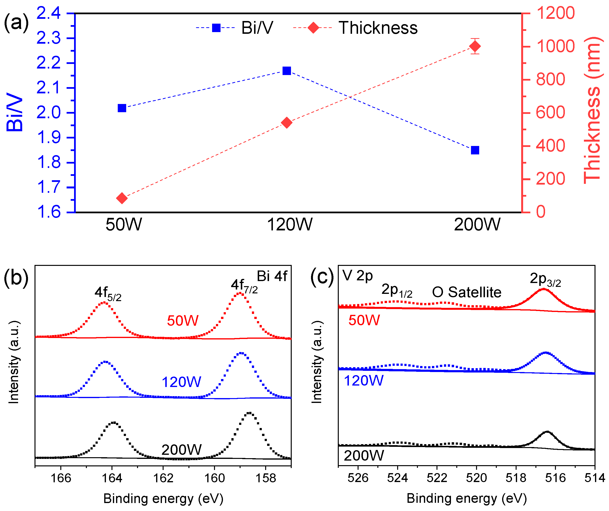
Abstract
1. Introduction
2. Materials and Methods
2.1. Deposition of BiVO4 Films
2.2. Characterization
3. Results and Discussion
3.1. Film Composition
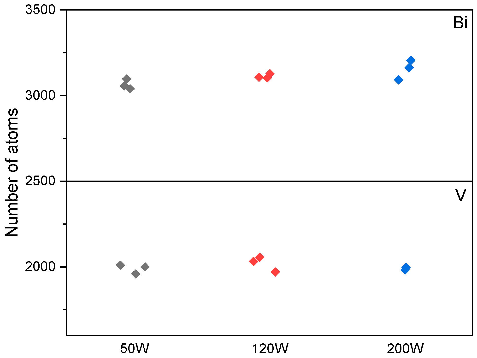
3.2. Monte Carlo Simulation
3.3. Sputtering Yield
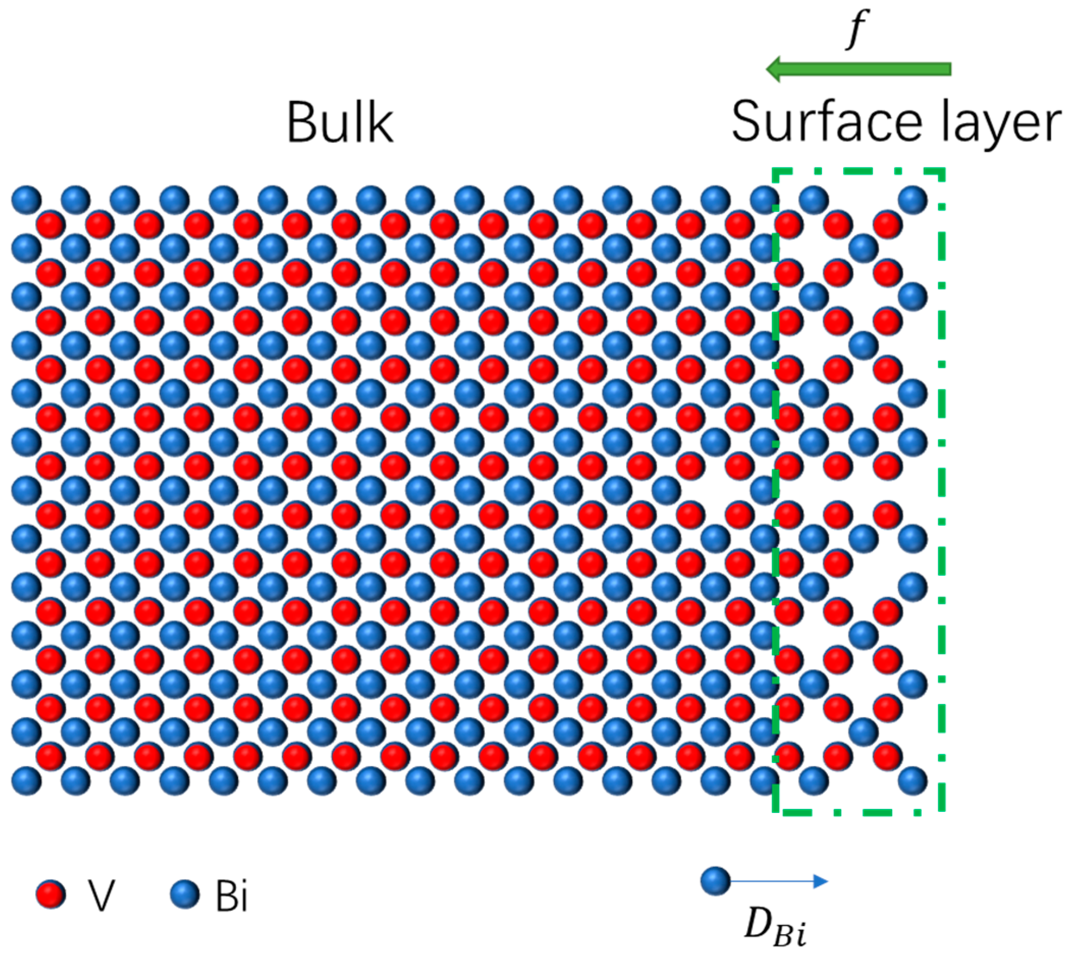
3.4. Adsorption on the Substrate
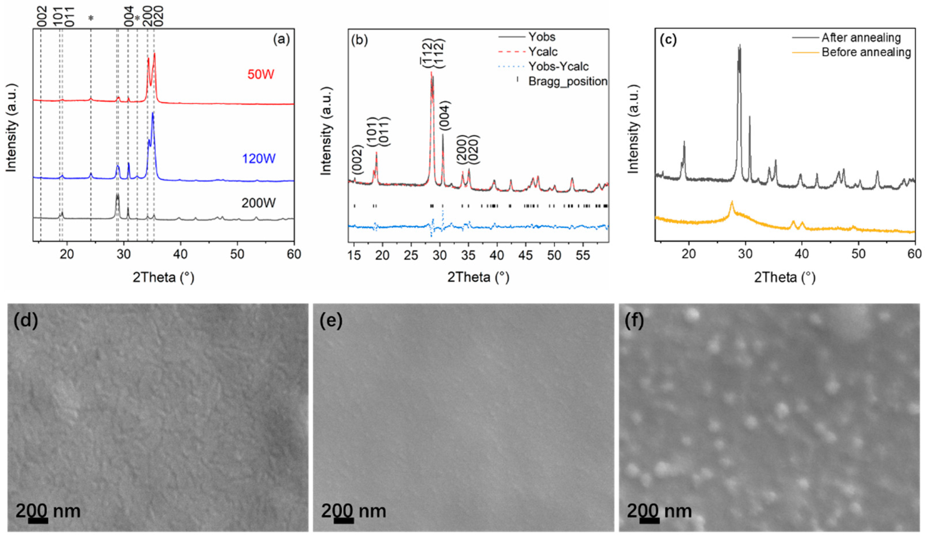
3.5. Structure and Morphology
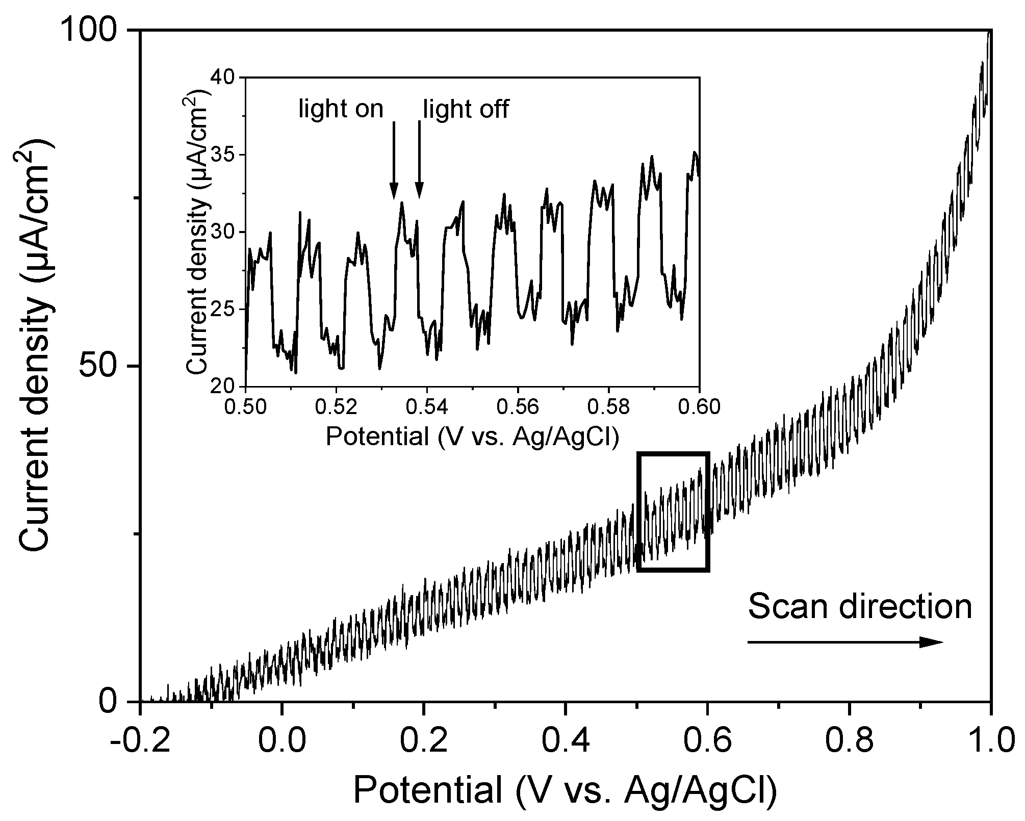
3.6. PEC Measurement
4. Conclusions
Supplementary Materials
Author Contributions
Funding
Institutional Review Board Statement
Informed Consent Statement
Data Availability Statement
Acknowledgments
Conflicts of Interest
References
- Lewis, N.S. Research opportunities to advance solar energy utilization. Science 2016, 351, aad1920. [Google Scholar] [CrossRef]
- Chen, S.; Wang, L. Thermodynamic Oxidation and Reduction Potentials of Photocatalytic Semiconductors in Aqueous Solution. Chem. Mater. 2012, 24, 3659–3666. [Google Scholar] [CrossRef]
- Tokunaga, S.; Kato, H.; Kudo, A. Selective Preparation of Monoclinic and Tetragonal BiVO4 with Scheelite Structure and Their Photocatalytic Properties. Chem. Mater. 2001, 13, 4624–4628. [Google Scholar] [CrossRef]
- Abdi, F.F.; Berglund, S.P. Recent developments in complex metal oxide photoelectrodes. J. Phys. D Appl. Phys. 2017, 50, 193002. [Google Scholar] [CrossRef]
- Cooper, J.K.; Gul, S.; Toma, F.M.; Chen, L.; Glans, P.A.; Guo, J.; Ager, J.W.; Yano, J.; Sharp, I.D. Electronic Structure of Monoclinic BiVO4. Chem. Mater. 2014, 26, 5365–5373. [Google Scholar] [CrossRef]
- Pihosh, Y.; Turkevych, I.; Mawatari, K.; Uemura, J.; Kazoe, Y. Photocatalytic generation of hydrogen by core-shell WO3/BiVO4 nanorods with ultimate water splitting efficiency. Sci. Rep. 2015, 1–2. [Google Scholar] [CrossRef]
- Dubal, D.P.; Jayaramulu, K.; Zboril, R.; Fischer, R.A.; Gomez-Romero, P. Unveiling BiVO4 nanorods as a novel anode material for high performance lithium ion capacitors: Beyond intercalation strategies. J. Mater. Chem. A 2018, 6, 6096–6106. [Google Scholar] [CrossRef]
- Coelho, D.; Gaudêncio, J.P.R.S.; Carminati, S.A.; Ribeiro, F.W.P.; Nogueira, A.F.; Mascaro, L.H. Bi electrodeposition on WO3 photoanode to improve the photoactivity of the WO3/BiVO4 heterostructure to water splitting. Chem. Eng. J. 2020, 399, 125836. [Google Scholar] [CrossRef]
- Wang, Y.; Shi, H.; Cui, K.; Zhang, L.; Ge, S.; Yu, J. Reversible electron storage in tandem photoelectrochemical cell for light driven unassisted overall water splitting. Appl. Catal. B Environ. 2020, 275, 119094. [Google Scholar] [CrossRef]
- Park, Y.; McDonald, K.J.; Choi, K.S. Progress in bismuth vanadate photoanodes for use in solar water oxidation. Chem. Soc. Rev. 2013, 42, 2321–2337. [Google Scholar] [CrossRef]
- Kang, D.; Kim, T.W.; Kubota, S.R.; Cardiel, A.C.; Cha, H.G.; Choi, K.S. Electrochemical Synthesis of Photoelectrodes and Catalysts for Use in Solar Water Splitting. Chem. Rev. 2015, 115, 12839–12887. [Google Scholar] [CrossRef] [PubMed]
- Barranco, A.; Borras, A.; Gonzalez-Elipe, A.R.; Palmero, A. Perspectives on oblique angle deposition of thin films: From fundamentals to devices. Prog. Mater. Sci. 2016, 76, 59–153. [Google Scholar] [CrossRef]
- Chen, L.; Alarcón-Lladó, E.; Hettick, M.; Sharp, I.D.; Lin, Y.; Javey, A.; Ager, J.W. Reactive Sputtering of Bismuth Vanadate Photoanodes for Solar Water Splitting. J. Phys. Chem. C 2013, 117, 21635–21642. [Google Scholar] [CrossRef]
- Pedroni, M.; Chiarello, G.L.; Haghshenas, N.; Canetti, M.; Ripamonti, D.; Selli, E.; Vassallo, E. Bismuth vanadate photoanodes for water splitting deposited by radio frequency plasma reactive co-sputtering. J. Vac. Sci. Technol. B 2019, 38, 12203. [Google Scholar] [CrossRef]
- Venkatesan, R.; Velumani, S.; Ordon, K.; Makowska-Janusik, M.; Corbel, G.; Kassiba, A. Nanostructured bismuth vanadate (BiVO4) thin films for efficient visible light photocatalysis. Mater. Chem. Phys. 2018, 205, 325–333. [Google Scholar] [CrossRef]
- Lamers, M.; Fiechter, S.; Friedrich, D.; Abdi, F.F.; van de Krol, R. Formation and suppression of defects during heat treatment of BiVO4 photoanodes for solar water splitting. J. Mater. Chem. A 2018, 6, 18694–18700. [Google Scholar] [CrossRef]
- Settaouti, A.; Settaouti, L. Simulation of the transport of sputtered atoms and effects of processing conditions. Appl. Surf. Sci. 2008, 254, 5750–5756. [Google Scholar] [CrossRef]
- Nichols, M.T.; Li, W.; Pei, D.; Antonelli, G.A.; Lin, Q.; Banna, S.; Nishi, Y.; Shohet, J.L. Measurement of bandgap energies in low-k organosilicates. J. Appl. Phys. 2014, 115, 94105. [Google Scholar] [CrossRef]
- Abrahamson, A.A. Born-Mayer-Type Interatomic Potential for Neutral Ground-State Atoms with Z = 2 to Z = 105. Phys. Rev. 1969, 178, 76–79. [Google Scholar] [CrossRef]
- Ishida, M.; Yamaguchi, Y.; Yoshinaga, H.; Yamamura, Y. Dynamical simulation of sputtering and reflection from a ternary alloy. Radiat. Eff. Defects Solids 1997, 142, 287–299. [Google Scholar] [CrossRef]
- Berg, S.; Katardjiev, I.V. Preferential sputtering effects in thin film processing. J. Vac. Sci. Technol. A 1999, 17, 1916–1925. [Google Scholar] [CrossRef]
- Carter, G.; Katardjiev, I.V.; Nobes, M.J. An altered layer model for sputter-profiling. Surf. Interface Anal. 1989, 14, 194–208. [Google Scholar] [CrossRef]
- Seah, M.P.; Clifford, C.A.; Green, F.M.; Gilmore, I.S. An accurate semi-empirical equation for sputtering yields I: For argon ions. Surf. Interface Anal. 2005, 37, 444–458. [Google Scholar] [CrossRef]
- Dam, B.; Rector, J.H.; Johansson, J.; Huijbregtse, J.; De Groot, D.G. Mechanism of incongruent ablation of SrTiO3. J. Appl. Phys. 1998, 83, 3386–3389. [Google Scholar] [CrossRef]
- Wasa, K.; Hayakawa, S. Handbook of Sputter Deposition Technology; Noyes Publications: Park Ridge, NJ, USA, 1992; pp. 78–84. ISBN 0-8155-1280-5. [Google Scholar]
- Asnin, L.D.; Chekryshkin, Y.S.; Fedorov, A.A. Calculation of the sticking coefficient in the case of the linear adsorption isotherm. Russ. Chem. Bull. 2003, 52, 2747–2749. [Google Scholar] [CrossRef]
- De Boer, J.H. Adsorption Phenomena; Frankenburg, W.G., Komarewsky, V.I., Rideal, E.K., Eds.; Academic Press: Cambridge, MA, USA, 1956; Volume 8, pp. 85–92. ISBN 0360-0564. [Google Scholar]
- Kölbach, M.; Harbauer, K.; Ellmer, K.; van de Krol, R. Elucidating the Pulsed Laser Deposition Process of BiVO4 Photoelectrodes for Solar Water Splitting. J. Phys. Chem. C 2020, 124, 4438–4447. [Google Scholar] [CrossRef]
- Gong, H.; Freudenberg, N.; Nie, M.; van de Krol, R.; Ellmer, K. BiVO4 photoanodes for water splitting with high injection efficiency, deposited by reactive magnetron co-sputtering. AIP Adv. 2016, 6, 45108. [Google Scholar] [CrossRef]
- Rietveld, H.M. Line profiles of neutron powder-diffraction peaks for structure refinement. Acta Crystallogr. 1967, 22, 151–152. [Google Scholar] [CrossRef]
- Sleight, A.W.; Chen, H.; Ferretti, A.; Cox, D. Crystal growth and structure of BiVO4 Locality: Synthetic Sample: T = 295 K. Mater. Res. Bull. 1979, 14, 1571–1581. [Google Scholar] [CrossRef]
- Abdi, F.F.; Firet, N.; van de Krol, R. Efficient BiVO4 Thin Film Photoanodes Modified with Cobalt Phosphate Catalyst and W-doping. ChemCatChem 2013, 5, 490–496. [Google Scholar] [CrossRef]
- Rettie, A.J.E.; Mozaffari, S.; McDaniel, M.D.; Pearson, K.N.; Ekerdt, J.G.; Markert, J.T.; Mullins, C.B. Pulsed Laser Deposition of Epitaxial and Polycrystalline Bismuth Vanadate Thin Films. J. Phys. Chem. C 2014, 118, 26543–26550. [Google Scholar] [CrossRef]


Publisher’s Note: MDPI stays neutral with regard to jurisdictional claims in published maps and institutional affiliations. |
© 2021 by the authors. Licensee MDPI, Basel, Switzerland. This article is an open access article distributed under the terms and conditions of the Creative Commons Attribution (CC BY) license (https://creativecommons.org/licenses/by/4.0/).
Share and Cite
Liu, J.; Tajima, K.; Abdellaoui, I.; Islam, M.M.; Ikeda, S.; Sakurai, T. Effect of Radio-Frequency Power on the Composition of BiVO4 Thin-Film Photoanodes Sputtered from a Single Target. Energies 2021, 14, 2122. https://doi.org/10.3390/en14082122
Liu J, Tajima K, Abdellaoui I, Islam MM, Ikeda S, Sakurai T. Effect of Radio-Frequency Power on the Composition of BiVO4 Thin-Film Photoanodes Sputtered from a Single Target. Energies. 2021; 14(8):2122. https://doi.org/10.3390/en14082122
Chicago/Turabian StyleLiu, Jiaqi, Kazuya Tajima, Imane Abdellaoui, Muhammad Monirul Islam, Shigeru Ikeda, and Takeaki Sakurai. 2021. "Effect of Radio-Frequency Power on the Composition of BiVO4 Thin-Film Photoanodes Sputtered from a Single Target" Energies 14, no. 8: 2122. https://doi.org/10.3390/en14082122
APA StyleLiu, J., Tajima, K., Abdellaoui, I., Islam, M. M., Ikeda, S., & Sakurai, T. (2021). Effect of Radio-Frequency Power on the Composition of BiVO4 Thin-Film Photoanodes Sputtered from a Single Target. Energies, 14(8), 2122. https://doi.org/10.3390/en14082122