
Switched Capacitor DC-DC Converters: A Survey on the Main Topologies, Design Characteristics, and Applications


Abstract
:1. Introduction
2. SC Structures
2.1. Greinacher Voltage Doubler (1914)
2.2. SC Voltage Doubler
2.3. Cockcroft Walton Voltage Multiplier or Ladder Structure (1932)
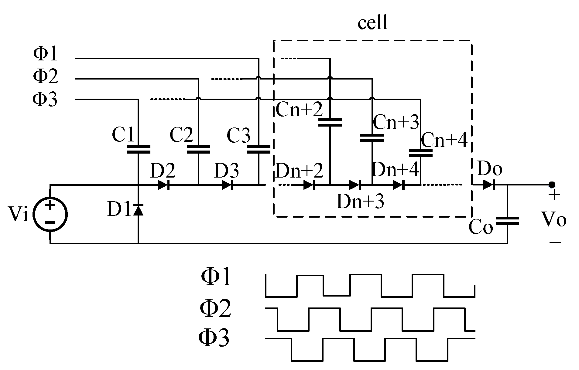
2.4. Series-Parallel Converter (1971)
2.5. Series-Parallel Multiphase Converter (1973)
2.6. Dickson Converter (1976)
2.7. Fibonacci Converter (1991)
2.8. Ladder Converter (1992)
3. Design Parameters
3.1. Components
3.1.1. Switches
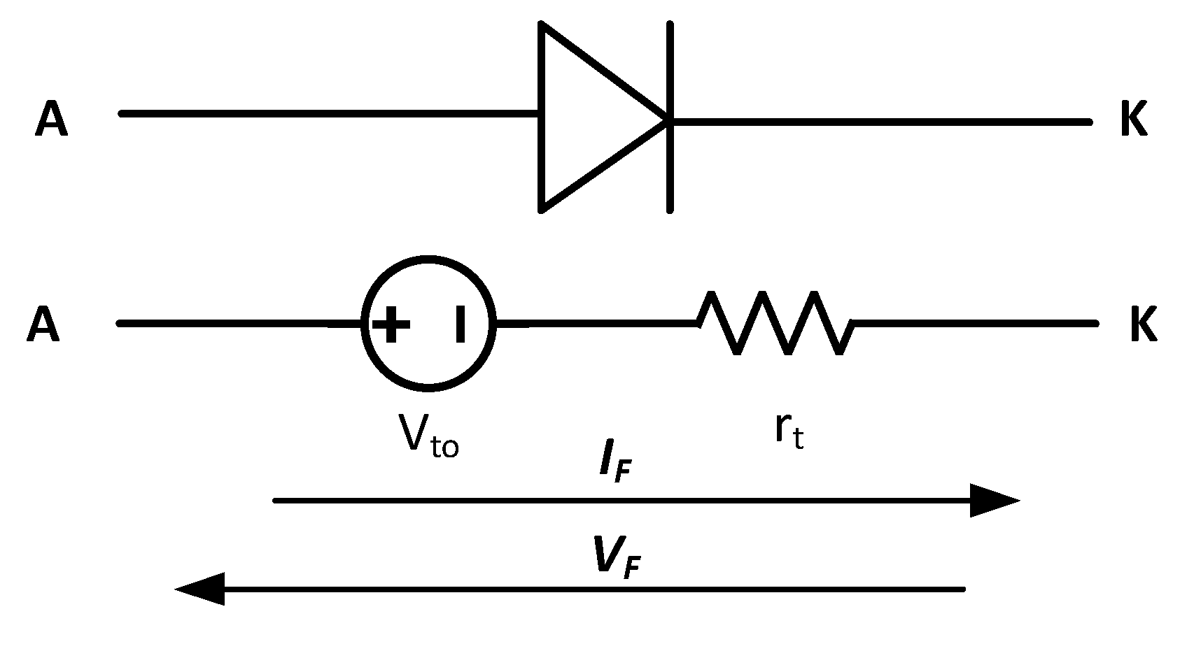
3.1.2. Diodes
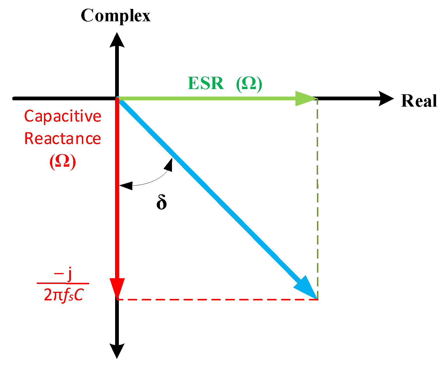
3.1.3. Capacitors
3.2. Operation Modes
- (1)
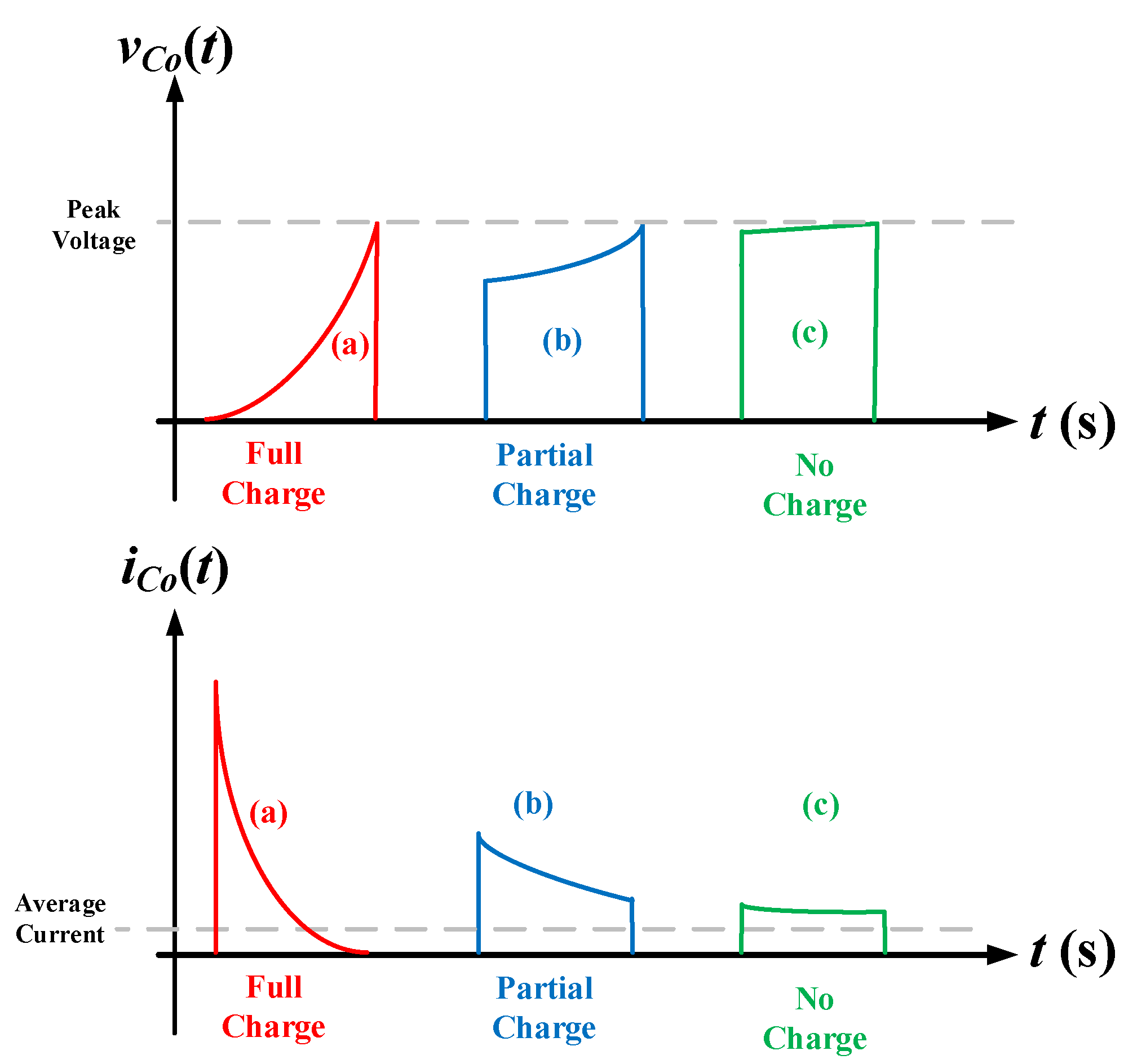
- If Ton >> RiCo, that is, when the time interval during which the switch remains on is much greater than the time constant of the circuit, the capacitors charge and discharge completely. Thus, the current becomes zero in each cycle, and then it can be assumed that the system operates under full charge condition according to Figure 19a.
- (2)
- (3)
- If the switching frequency is very high, that is, if the value of Ton is small in relation to Ts, then Ton << RiCo. Thus, the current in the capacitor is almost zero, and the voltage across it can also be considered constant. In this mode, the converter operates at no charge condition according to Figure 19c.
- (1)
- If β > 1, the converter operates in full charge mode, where Ton > 5τ, while the output resistance depends on the inverse of the product of fs and Co. In other words, the resistances of the switches and capacitors represented by Ri has little influence on the converter behavior.
- (2)
- If β = 1, the capacitors operate in partial charge mode and the output resistance of the converter depends on Ri, Co, and fs.
- (3)
- If β < 1, the converter operates in no charge mode. In this case, it is possible to employ very short switching time intervals compared to the circuit time constant. Thus, the output resistance of the converter is very dependent on Ri and D.
3.3. Voltage Balance
3.4. Efficiency
3.5. Regulation and Control
3.6. Comparison among SC Topologies
4. Applications

| IC | Vi (V) | Io (mA) | ηmax (%) | |
|---|---|---|---|---|
| MAX660 [180] | 1.8 to 5.5 | 100 | 88 | |
| LM2660 [184] | 2.5 to 5.5 | 100 | 88 | |
| LM2685 [185] | 2.85 to 6.5 | 50 | 80 | |
| MAX1680 [186] | 2 to 5.5 | 5 | 90 | |
| MAX860 [187] | 2 to 5.5 | 50 | 87 | |
| LT1054 [188] | 3.5 to 15 | 100 | NA | |
| LM2665 [189] | 2.5 to 5.5 | 40 | 90 | |
| LM2767 [190] | 1.8 to 5.5 | 15 | 96 | |
| ADP3610 [191] | 3 to 3.6 | 320 | 90 | |
| TCM828 [192] | 1.5 to 5.5 | 25 | 95 | |
| GS7660 [193] | 3 to 6 | 200 | 98 |
5. Conclusions
Author Contributions
Funding
Data Availability Statement
Acknowledgments
Conflicts of Interest
References
- Bose, B.K. Global energy scenario and impact of power electronics in 21st century. IEEE Trans. Ind. Electron. 2013, 60, 2638–2651. [Google Scholar] [CrossRef]
- Baliga, B.J. Trends in power semiconductor devices. IEEE Trans. Electron. Devices 1996, 43, 1717–1731. [Google Scholar] [CrossRef]
- Bose, B.K. Evaluation of modern power semiconductor devices and future trends of converters. IEEE Trans. Ind. Appl. 1992, 28, 403–413. [Google Scholar] [CrossRef]
- Biela, J.; Schweizer, M.; Waffler, S.; Kolar, J.W. SiC versus Si—evaluation of potentials for performance improvement of inverter and DC–DC converter systems by SiC power semiconductors. IEEE Trans. Ind. Electron. 2011, 58, 2872–2882. [Google Scholar] [CrossRef]
- Zhan, A.; Dang, G.T.; Ren, F.; Cho, H.; Lee, K.-P.; Pearton, S.J.; Chyi, J.-I.; Nee, T.-Y.; Chuo, C.-C. Comparison of GaN pin and Schottky rectifier performance. IEEE Trans. Electron Devices 2001, 48, 407–411. [Google Scholar] [CrossRef]
- Chowdhury, S.; Stum, Z.; Li, Z.D.; Ueno, K.; Chow, T.P. Comparison of 600V Si, SiC and GaN power devices. Mater. Sci. Forum 2014, 778–780, 971–974. [Google Scholar] [CrossRef]
- González, A.; Goikolea, E.; Barrena, J.A.; Mysyk, R. Review on supercapacitors: Technologies and materials. Renew. Sustain. Energy Rev. 2016, 58, 1189–1206. [Google Scholar] [CrossRef]
- Zubieta, L.; Bonert, R. Characterization of double-layer capacitors (DLCs) for power electronics applications. In Proceedings of the Conference Record of 1998 IEEE Industry Applications Conference. Thirty-Third IAS Annual Meeting (Cat. No.98CH36242), Saint Louis, MO, USA, 12–15 October 1998; Volume 2, pp. 1149–1154. [Google Scholar]
- Shokrollahi, H.; Janghorban, K. Soft magnetic composite materials (SMCs). J. Mater. Process. Technol. 2007, 189, 1–12. [Google Scholar] [CrossRef]
- Kunz, W.; Grätzer, D. Amorphous alloys for switched-mode power supplies. J. Magn. Magn. Mater. 1980, 19, 183–184. [Google Scholar] [CrossRef]
- Li, Z.; Yao, K.; Li, D.; Ni, X.; Lu, Z. Core loss analysis of Finemet type nanocrystalline alloy ribbon with different thickness. Prog. Nat. Sci. Mater. Int. 2017, 27, 588–592. [Google Scholar] [CrossRef]
- Texas Instruments. LM2750 Low-Noise Switched-Capacitor Boost Regulator. Available online: http://www.ti.com/lit/ds/symlink/lm2750.pdf (accessed on 1 March 2021).
- ON Semiconductor. NCP 1719 Switched Capacitor Voltage Inverter. Available online: https://www.onsemi.com/pub/Collateral/NCP1729-D.PDF (accessed on 1 March 2021).
- Tan, S.-C.; Nur, M.; Kiratipongvoot, S.; Bronstein, S.; Lai, Y.-M.; Tse, C.; Ioinovici, A. Switched-capacitor converter configuration with low EMI emission obtained by interleaving and its large-signal modeling. In Proceedings of the 2009 IEEE International Symposium on Circuits and Systems, Taipei, Taiwan, 24–27 May 2009; pp. 1081–1084. [Google Scholar]
- Ioinovici, A. Switched-capacitor power electronics circuits. IEEE Circ. Syst. Mag. 2001, 1, 37–42. [Google Scholar] [CrossRef]
- Tsai, K.; Qi, F.; Davidson, E.; Xu, L. Common mode EMI noise characterization and improvement for GaN switched-capacitor converter. In Proceedings of the IEEE Energy Conversion Congress and Exposition, Denver, CO, USA, 15–19 September 2013; pp. 4159–4165. [Google Scholar]
- Zhu, G.; Ioinovici, A. Steady-state characteristics of switched-capacitor electronic converters. J. Circ. Syst. Comput. 1997, 7, 69–91. [Google Scholar] [CrossRef]
- Guangyong, Z.; Ioinovici, A. Switched-capacitor power supplies: DC voltage ratio, efficiency, ripple, regulation. In Proceedings of the IEEE International Symposium on Circuits and Systems (ISCAS), Atlanta, GA, USA, 15 May 1996; pp. 553–556. [Google Scholar]
- Zhu, G.; Wei, H.; Batarseh, I.; Ioinovici, A. A new switched-capacitor dc-dc converter with improved line and load regulations. In Proceedings of the IEEE International Symposium on Circuits and Systems (ISCAS), Orlando, FL, USA, 30 May–2 June 1999; pp. 234–237. [Google Scholar]
- Das, R.; Seo, G.; Le, H. Analysis of dual-inductor hybrid converters for extreme conversion ratios. IEEE J. Emerg. Sel. Top. Power Electron. 2020, 1–13. [Google Scholar] [CrossRef]
- Assem, P.; Liu, W.; Lei, Y.; Hanumolu, P.K.; Pilawa-Podgurski, R.C.N. Hybrid Dickson switched-capacitor converter with wide conversion ratio in 65-nm CMOS. IEEE J. Solid State Circ. 2020, 55, 2513–2528. [Google Scholar] [CrossRef]
- Oualkadi, A.E.; Cordeau, D.; Paillot, J. High-Q CMOS LC pseudo switched-capacitor bandpass filter with center frequency tuning. In Proceedings of the IEEE International Symposium on Circuits and Systems, Kos, Greece, 21–24 May 2006; p. 3909. [Google Scholar]
- Ye, Z.; Lei, Y.; Pilawa-Podgurski, R.C.N. The cascaded resonant converter: A hybrid switched-capacitor topology with high power density and efficiency. IEEE Trans. Power Electron. 2020, 35, 4946–4958. [Google Scholar] [CrossRef]
- Ura, K. Contrast mechanism of negatively charged insulators in scanning electron microscope. Microscopy 1998, 47, 143–147. [Google Scholar] [CrossRef]
- Iqbal, S.; Singh, G.K.; Besar, R. A dual-mode input voltage modulation control scheme for voltage multiplier based X-ray power supply. IEEE Trans. Power Electron. 2008, 23, 1003–1008. [Google Scholar] [CrossRef]
- Sun, J.; Ding, X.; Nakaoka, M.; Takano, H. Series resonant ZCS–PFM DC–DC converter with multistage rectified voltage multiplier and dual-mode PFM control scheme for medical-use high-voltage X-ray power generator. IEE Proc. Electr. Power Appl. 2000, 147, 527–534. [Google Scholar] [CrossRef]
- Ahmed, F.U.; Chowdhury, M.H. An asynchronous reconfigurable switched capacitor voltage regulator. In Proceedings of the IEEE 61st International Midwest Symposium on Circuits and Systems (MWSCAS), Windsor, ON, Canada, 5–8 August 2018; pp. 1110–1113. [Google Scholar]
- Chen, C.; Liu, X. A high-efficiency switched capacitor converter for always-on block. In Proceedings of the 14th IEEE International Conference on Solid State and Integrated Circuit Technology (ICSICT), Qingdao, China, 31 October–3 November 2018; pp. 1–3. [Google Scholar]
- Lei, H.; Hao, R.; You, X.; Li, F.; Zhou, M. Nonisolated high step-up soft-switching DC-DC converter integrating Dickson switched-capacitor techniques. In Proceedings of the IEEE Energy Conversion Congress and Exposition (ECCE), Portland, OR, USA, 23–27 September 2018; pp. 1247–1252. [Google Scholar]
- Jiang, J.; Liu, X.; Ki, W.; Mok, P.K.T.; Lu, Y. A multiphase switched-capacitor converter for fully integrated AMLED microdisplay system. IEEE Trans. Power Electron. 2020, 35, 6001–6011. [Google Scholar] [CrossRef]
- Shah, N.; Lajevardi, P.; Wojciechowski, K.; Lang, C.; Murmann, B. An energy harvester using image sensor pixels with cold start and over 96% MPPT efficiency. IEEE Solid State Circ. Lett. 2019, 2, 207–210. [Google Scholar] [CrossRef]
- Chiou, C.W.; Sun, Y.; Lee, C.; Liou, J. Low-complexity unidirectional systolic Dickson basis multiplier for lightweight cryptosystems. Electron. Lett. 2019, 55, 28–30. [Google Scholar] [CrossRef]
- Gunnam, L.C.; Lai, Y.; Sung, G. Differential Dickson voltage multiplier with matching network for radio frequency harvester. In Proceedings of the IEEE International Conference on Consumer Electronics, Taiwan (ICCE-TW), Taipei, Taiwan, 12–14 June 2017; pp. 417–418. [Google Scholar]
- Dela Cruz, S.; delos Reyes, M.G.; Alvarez, A.; de Leon, M.T.; Roque, C.R. Design and implementation of passive RF-DC converters for RF power harvesting systems. In Proceedings of the TENCON, 2010 IEEE Region 10 Conference, Fukoka, Japan, 21–24 November 2010; pp. 1503–1508. [Google Scholar]
- Forouzesh, M.; Siwakoti, Y.P.; Gorji, S.A.; Blaabjerg, F.; Lehman, B. Step-up DC–DC converters: A comprehensive review of voltage-boosting techniques, topologies, and applications. IEEE Trans. Power Electron. 2017, 32, 9143–9178. [Google Scholar] [CrossRef]
- Arfin, S.; Mamun, A.A.; Chowdhury, T.; Sarowar, G. Zeta based hybrid DC-DC converter using switched inductor and switched capacitor combined structure for high gain applications. In Proceedings of the IEEE International Conference on Power, Electrical, and Electronics and Industrial Applications (PEEIACON), Dhaka, Bangladesh, 29 November–1 December 2019; pp. 1–4. [Google Scholar]
- Axelrod, B.; Berkovich, Y.; Ioinovici, A. Switched-capacitor (SC)/switched inductor (SL) structures for getting hybrid step-down Cuk/Sepic/Zeta converters. In Proceedings of the IEEE International Symposium on Circuits and Systems, Kos, Greece, 21–24 May 2006; p. 4. [Google Scholar]
- Banaei, M.R.; Kazemi, F.M. A modified selective harmonic elimination switching strategy for Hybrid Flying Capacitor Multicell converter. In Proceedings of the 7th International Conference on Electrical and Electronics Engineering (ELECO), Bursa, Turkey, 1–4 December 2011; pp. I-278–I-282. [Google Scholar]
- Bhaskar, M.; Ganesan, R.G.; Narayanan, K. Interleaved hybrid boost converter with switched capacitor technique. In Proceedings of the IEEE Innovative Smart Grid Technologies, Asia (ISGT Asia), Chengdu, China, 21–24 May 2019; pp. 3890–3895. [Google Scholar]
- Chen, M.; Hu, J.; Li, K.; Ioinovici, A. A new switched-capacitor based hybrid converter with large step-up DC gain and low voltage on its semiconductors. In Proceedings of the IEEE International Symposium on Circuits and Systems (ISCAS), Montreal, QC, Canada, 22–25 May 2016; pp. 1190–1193. [Google Scholar]
- Chen, M.; Li, K.; Hu, J.; Ioinovici, A. Hybrid switched-capacitor quadratic boost converters with very high DC gain and low voltage stress on their semiconductor devices. In Proceedings of the IEEE Energy Conversion Congress and Exposition (ECCE), Milwaukee, WI, USA, 18–22 September 2016; pp. 1–8. [Google Scholar]
- Dantas, M.; Oliveira, F.; Albuquerque, L.; Freitas, I.; Andersen, R. A hybrid bidirectional push-pull DC-DC converter with a ladder switched-capacitor cell. In Proceedings of the IEEE 15th Brazilian Power Electronics Conference and 5th IEEE Southern Power Electronics Conference (COBEP/SPEC), Santos, Brazil, 1–4 December 2019; pp. 1–6. [Google Scholar]
- Eate, V.K.; Veerachary, M. Analysis of two-input Switched Inductor-Capacitor Hybrid Buck-SEPIC DC-DC converter. In Proceedings of the IEEE Transportation Electrification Conference (ITEC-India), Pune, India, 13–15 December 2017; pp. 1–6. [Google Scholar]
- Hulea, D.; Muntean, N.; Gireada, M.; Cornea, O. A bidirectional hybrid switched-capacitor DC-DC converter with a high voltage gain. In Proceedings of the International Aegean Conference on Electrical Machines and Power Electronics (ACEMP) & 2019 International Conference on Optimization of Electrical and Electronic Equipment (OPTIM), Istanbul, Turkey, 27–29 August 2019; pp. 289–296. [Google Scholar]
- Hulea, D.; Muntean, N.; Gireada, M.; Cornea, O.; Serban, E. Bidirectional hybrid switched-inductor switched-capacitor converter topology with high voltage gain. In Proceedings of the 21st European Conference on Power Electronics and Applications (EPE 2019 ECCE Europe), Genova, Italy, 3–5 September 2019; pp. 1–10. [Google Scholar]
- Janabi, A.; Wang, B. Switched-capacitor voltage boost converter for electric and hybrid electric vehicle drives. IEEE Transact. Power Electron. 2020, 35, 5615–5624. [Google Scholar] [CrossRef]
- Li, S.; Zheng, Y.; Wu, B.; Smedley, K.M. A family of resonant two-switch boosting switched-capacitor converter with ZVS operation and a wide line regulation range. IEEE Transact. Power Electron. 2018, 33, 448–459. [Google Scholar] [CrossRef]
- Kumar, P.; Veerachary, M. Hybrid switched inductor/switched capacitor based quasi-Z-source DC-DC boost converter. In Proceedings of the 2nd IEEE International Conference on Power Electronics, Intelligent Control and Energy Systems (ICPEICES), Delhi, India, 22–24 October 2018; pp. 617–622. [Google Scholar]
- Leandro, G.M.; Barbi, I. DC-DC hybrid switched-capacitor LLC resonant converter: All switches with VDS=Vin/2. In Proceedings of the IEEE PES Innovative Smart Grid Technologies Conference–Latin America (ISGT Latin America), Gramado, Brazil, 15–18 September 2019; pp. 1–6. [Google Scholar]
- Lei, Y.; Liu, W.; Pilawa-Podgurski, R.C.N. An analytical method to evaluate flying capacitor multilevel converters and hybrid switched-capacitor converters for large voltage conversion ratios. In Proceedings of the IEEE 16th Workshop on Control and Modeling for Power Electronics (COMPEL), Vancouver, BC, Canada, 12–15 July 2015; pp. 1–7. [Google Scholar]
- Lei, Y.; Liu, W.; Pilawa-Podgurski, R.C.N. An analytical method to evaluate and design hybrid switched-capacitor and multilevel converters. IEEE Trans. Power Electron. 2018, 33, 2227–2240. [Google Scholar] [CrossRef]
- Lei, Y.; Ye, Z.; Pilawa-Podgurski, R.C.N. A GaN-based 97% efficient hybrid switched-capacitor converter with lossless regulation capability. In Proceedings of the IEEE Energy Conversion Congress and Exposition (ECCE), Montreal, QC, Canada, 20–24 September 2015; pp. 4264–4270. [Google Scholar]
- Li, G.; Zhiming, C.; Jian, L. Design of a hybrid monolithic integrated switched capacitor DC-DC step-up converter. In Proceedings of the IPEMC 2000. Third International Power Electronics and Motion Control Conference (IEEE Cat. No.00EX435), Beijing, China, 15–18 August 2000; pp. 263–266. [Google Scholar]
- Pelan, O.; Muntean, N.; Cornea, O. Comparative evaluation of buck and switched-capacitor hybrid buck DC-DC converters. In Proceedings of the International Symposium on Power Electronics Power Electronics, Electrical Drives, Automation and Motion, Sorrento, Italy, 20–22 June 2012; pp. 1330–1335. [Google Scholar]
- Sadigh, A.K.; Dargahi, V.; Corzine, K.A. Reduction of switches and flying capacitors in a hybrid topology of the stacked multicell converters. In Proceedings of the IECON 2019, 45th Annual Conference of the IEEE Industrial Electronics Society, Lisbon, Portugal, 14–17 October 2019; pp. 4977–4982. [Google Scholar]
- Sarath, R.; Kanakasabapathy, P. Switched-capacitor/switched-inductor Ćuk-derived hybrid converter for nanogrid applications. In Proceedings of the International Conference on Computation of Power, Energy, Information and Communication (ICCPEIC), Melmaruvathur, India, 22–23 April 2015; pp. 430–435. [Google Scholar]
- Soares, M.V.; Lambert, G.; Novaes, Y.R. Hybrid switched capacitor DC-DC converter based on MMC. In Proceedings of the IEEE 15th Brazilian Power Electronics Conference and 5th IEEE Southern Power Electronics Conference (COBEP/SPEC), Santos, Brazil, 1–4 December 2019; pp. 1–6. [Google Scholar]
- Stewart, J.; Richards, J.; Delhotal, J.; Neely, J.; Flicker, J.; Brocato, R.; Rashkin, L. Design and evaluation of hybrid switched capacitor converters for high voltage, high power density applications. In Proceedings of the IEEE Applied Power Electronics Conference and Exposition (APEC), San Antonio, TX, USA, 4–8 March 2018; pp. 105–112. [Google Scholar]
- Tewari, N.; Sreedevi, V.T. Switched inductor-switched capacitor based high gain hybrid dc-dc converter. In Proceedings of the 8th IEEE India International Conference on Power Electronics (IICPE), Jaipur, India, 13–15 December 2018; pp. 1–6. [Google Scholar]
- Vecchia, M.D.; Lazzarin, T.B. A hybrid switched capacitor DC-DC buck converter. In Proceedings of the IEEE 13th Brazilian Power Electronics Conference and 1st Southern Power Electronics Conference (COBEP/SPEC), Fortaleza, Brazil, 29 November–2 December 2015; pp. 1–6. [Google Scholar]
- Vecchia, M.D.; Lazzarin, T.B. Hybrid DC-DC buck converter with active switched capacitor cell and low voltage gain. In Proceedings of the IEEE Energy Conversion Congress and Exposition (ECCE), Milwaukee, WI, USA, 18–22 September 2016; pp. 1–6. [Google Scholar]
- Veerachary, M.; Reddy, T.N. Voltage-mode control of hybrid switched capacitor converters. In Proceedings of the IECON 2006, 32nd Annual Conference on IEEE Industrial Electronics, Paris, France, 6–10 November 2006; pp. 2450–2453. [Google Scholar]
- Veerachary, M.; Reddy, T.N. Design and control of hybrid switched capacitor DC-DC converter with different operating conditions. In Proceedings of the International Conference on Advances in Computing, Control, and Telecommunication Technologies, Bangalore, India, 28–29 December 2009; pp. 559–563. [Google Scholar]
- Veerachary, M.; Sudhakar, S.B. Peak-current mode control of hybrid switched capacitor converter. In Proceedings of the International Conference on Power Electronic, Drives and Energy Systems, New Delhi, India, 12–15 December 2006; pp. 1–6. [Google Scholar]
- Xiong, S.; Tan, S.; Wong, S. Analysis of a high-voltage-gain hybrid switched-capacitor buck converter. In Proceedings of the IEEE International Symposium of Circuits and Systems (ISCAS), Rio de Janeiro, Brazil, 15–18 May 2011; pp. 1616–1619. [Google Scholar]
- Greinacher, H. The ionometer and its application to the measurement of radium and röntgen rays. Phys. Z. 1914, 15, 410–415. [Google Scholar]
- Kind, D.; Feser, K. High Voltage Test Techniques; Elsevier: Amsterdam, The Netherlands, 2001. [Google Scholar]
- Hwang, F.; Shen, Y.; Jayaram, S.H. Low-ripple compact high-voltage DC power supply. IEEE Trans. Ind. Appl. 2006, 42, 1139–1145. [Google Scholar] [CrossRef]
- Fukuyama, T.; Sugihara, K. Study on operating principle of Cockcroft-Walton circuit to produce plasmas using high-voltage discharge. Plasma Fusion Res. 2016, 11, 2401008. [Google Scholar] [CrossRef] [Green Version]
- Midya, P. Efficiency analysis of switched capacitor doubler. In Proceedings of the 39th Midwest Symposium on Circuits and Systems, Ames, IA, USA, 21–21 August 1996; pp. 1019–1022. [Google Scholar]
- Cataldo, G.D.; Palumbo, G. Double and triple charge pump for power IC: Dynamic models which take parasitic effects into account. In IEEE Transactions on Circuits and Systems I: Fundamental Theory and Applications; IEEE: Piscataway, NJ, USA, 1993; Volume 40, pp. 92–101. [Google Scholar]
- Cockcroft, J.D.; Walton, E.T. Experiments with high velocity positive ions. (I) Further developments in the method of obtaining high velocity positive ions. Proc. Math. Phys. Eng. Sci. 1932, 136, 619–630. [Google Scholar]
- Müller, L.; Kimball, J.W. Dual-input high gain DC-DC converter based on the Cockcroft-Walton multiplier. In Proceedings of the IEEE Energy Conversion Congress and Exposition (ECCE), Pittsburgh, PA, USA, 14–18 September 2014; pp. 5360–5367. [Google Scholar]
- Müller, L.; Kimball, J.W. High gain DC–DC converter based on the Cockcroft–Walton multiplier. IEEE Trans. Power Electron. 2016, 31, 6405–6415. [Google Scholar] [CrossRef]
- Young, C.; Chen, M. A novel single-phase ac to high voltage dc converter based on Cockcroft-Walton cascade rectifier. In Proceedings of the International Conference on Power Electronics and Drive Systems (PEDS), Taipei, Taiwan, 2–5 November 2009; pp. 822–826. [Google Scholar]
- Young, C.; Chun-Cho, K.; Chen, M.; Chao-Cheng, W. A Cockcroft-Walton voltage multiplier with PFC using ZC-ZVT auxiliary circuit. In Proceedings of the IECON 2011, 37th Annual Conference of the IEEE Industrial Electronics Society, Melbourne, VIC, Australia, 7–10 November 2011; pp. 1000–1005. [Google Scholar]
- Young, C.; Chen, M.; Hong-Lin, C.; Jen-Yi, C.; Chun-Cho, K. Transformerless single-stage high step-up AC-DC converter based on symmetrical Cockcroft-Walton voltage multiplier with PFC. In Proceedings of the IEEE Ninth International Conference on Power Electronics and Drive Systems, Singapore, 5–8 December 2011; pp. 191–196. [Google Scholar]
- Kobougias, I.C.; Tatakis, E.C. Optimal design of a half-wave Cockroft-Walton voltage multiplier with different capacitances per stage. IEEE Transact. Power Electron. 2010, 25, 2460–2468. [Google Scholar] [CrossRef]
- Brugler, J.S. Theoretical performance of voltage multiplier circuits. IEEE J. Solid State Circ. 1971, 6, 132–135. [Google Scholar] [CrossRef]
- Tanzawa, T. On-Chip High-Coltage Generator Design; Springer: Berlin/Heidelberg, Germany, 2013. [Google Scholar]
- Falkner, A. Generalised cockcroft-walton voltage multipliers. Electron. Lett. 1973, 9, 585–586. [Google Scholar] [CrossRef]
- Dickson, J.F. On-chip high-voltage generation in MNOS integrated circuits using an improved voltage multiplier technique. IEEE J. Solid State Circ. 1976, 11, 374–378. [Google Scholar] [CrossRef]
- Alzahrani, A.; Shamsi, P.; Ferdowsi, M. Analysis and design of bipolar Dickson DC-DC converter. In Proceedings of the IEEE Power and Energy Conference at Illinois (PECI), Champaign, IL, USA, 23–24 February 2017; pp. 1–6. [Google Scholar]
- Tanzawa, T.; Tanaka, T. A dynamic analysis of the Dickson charge pump circuit. IEEE J. Solid State Circ. 1997, 32, 1231–1240. [Google Scholar] [CrossRef]
- Tanzawa, T. A switch-resistance-aware Dickson charge pump model for optimizing clock frequency. IEEE Trans. Circ. Syst. II Express Briefs 2011, 58, 336–340. [Google Scholar] [CrossRef]
- Makowski, M.S.; Maksimovic, D. Performance limits of switched-capacitor DC-DC converters. In Proceedings of the PESC 1995, Power Electronics Specialist Conference, Atlanta, GA, USA, 18–22 June 1995; pp. 1215–1221. [Google Scholar]
- Makowski, M.S. Realizability conditions and bounds on synthesis of switched-capacitor DC-DC voltage multiplier circuits. IEEE Trans. Circ. Syst. I Regul. Pap. 1997, 44, 684–691. [Google Scholar] [CrossRef]
- Meynard, T.A.; Foch, H. Multi-level conversion: High voltage choppers and voltage-source inverters. In Proceedings of the PESC 19992 Record, 23rd Annual IEEE Power Electronics Specialists Conference, Toledo, Spain, 29 June–3 July 1992; pp. 397–403. [Google Scholar]
- Meynard, T.A.; Foch, H.; Thomas, P.; Courault, J.; Jakob, R.; Nahrstaedt, M. Multicell converters: Basic concepts and industry applications. IEEE Trans. Ind. Electron. 2002, 49, 955–964. [Google Scholar] [CrossRef]
- Lazzarin, T.B.; Andersen, R.L.; Martins, G.B.; Barbi, I. A 600-W switched-capacitor AC–AC converter for 220 V/110 V and 110 V/220 V applications. IEEE Trans. Power Electron. 2012, 27, 4821–4826. [Google Scholar] [CrossRef]
- Östling, M.; Ghandi, R.; Zetterling, C. SiC power devices–Present status, applications and future perspective. In Proceedings of the IEEE 23rd International Symposium on Power Semiconductor Devices and ICs, San Diego, CA, USA, 23–26 May 2011; pp. 10–15. [Google Scholar]
- Tanabe, H.; Kojima, T.; Imakiire, A.; Fuji, K.; Kozako, M.; Hikita, M. Comparison performance of Si-IGBT and SiC-MOSFET used for high efficiency inverter of contactless power transfer system. In Proceedings of the IEEE 11th International Conference on Power Electronics and Drive Systems, Sydney, NSW, Australia, 9–12 June 2015; pp. 707–710. [Google Scholar]
- Wang, G.; Wang, F.; Magai, G.; Lei, Y.; Huang, A.; Das, M. Performance comparison of 1200V 100A SiC MOSFET and 1200V 100A silicon IGBT. In Proceedings of the IEEE Energy Conversion Congress and Exposition, Denver, CO, USA, 15–19 September 2013; pp. 3230–3234. [Google Scholar]
- Baliga, B.J. Fundamentals of Power Semiconductor Devices; Springer: Berlin/Heidelberg, Germany, 2010. [Google Scholar]
- Rashid, M.H. Power Electronics Handbook: Devices, Circuits and Applications; Elsevier: Amsterdam, The Netherlands, 2010. [Google Scholar]
- Ahmed, A. Power Electronics for Technology; Pearson: New York, NY, USA, 1998. [Google Scholar]
- Ye, Y.; Chen, S.; Yi, Y. Switched-capacitor and coupled-inductor based high step-up converter with improved voltage gain. IEEE J. Emerg. Sel. Top. Power Electron. 2021, 9, 754–764. [Google Scholar] [CrossRef]
- Harada, K.; Katsuki, A.; Fujiwara, M. Use of ESR for deterioration diagnosis of electrolytic capacitor. IEEE Trans. Power Electron. 1993, 8, 355–361. [Google Scholar] [CrossRef]
- Ahmad, M. A simple scheme for loss angle measurement of a capacitor. IEEE Trans. Energy Convers. 2004, 19, 228–229. [Google Scholar] [CrossRef]
- Ramm, G.; Moser, H. From the calculable AC resistor to capacitor dissipation factor determination on the basis of time constants. IEEE Trans. Instrum. Meas. 2001, 50, 286–289. [Google Scholar] [CrossRef]
- Fiore, R. ESR Losses in Ceramic Capacitors. Available online: www.atceramics.com (accessed on 1 March 2021).
- Roy, T.; Smith, L.; Prymak, J. ESR and ESL of ceramic capacitor applied to decoupling applications. In Proceedings of the IEEE 7th Topical Meeting on Electrical Performance of Electronic Packaging (Cat. No.98TH8370), West Point, NY, USA, 26–28 October 1998; pp. 213–216. [Google Scholar]
- Gebbia, M. Low ESR capacitors: Fact or fiction? ECN Luty 2001, 200. [Google Scholar]
- Anderson, R. Select the right plastic film capacitor for your power electronic applications. In Proceedings of the IAS 1996, Conference Record of the 1996 IEEE Industry Applications Conference Thirty-First IAS Annual Meeting, San Diego, CA, USA, 6–10 October 1996; pp. 1327–1330. [Google Scholar]
- Tortai, J.; Denat, A.; Bonifaci, N. Self-healing of capacitors with metallized film technology: Experimental observations and theoretical model. J. Electrost. 2001, 53, 159–169. [Google Scholar] [CrossRef]
- Borghetti, A.; Nucci, C.A.; Pasini, G.; Pirani, S.; Rinaldi, M. Tests on self-healing metallized polypropylene capacitors for power applications. IEEE Trans. Power Deliv. 1995, 10, 556–561. [Google Scholar] [CrossRef]
- Chen, Y.; Li, H.; Lin, F.; Lv, F.; Zhang, M.; Li, Z.; Liu, D. Study on self-healing and lifetime characteristics of metallized-film capacitor under high electric field. IEEE Trans. Plasma Sci. 2012, 40, 2014–2019. [Google Scholar] [CrossRef]
- Makdessi, M.; Sari, A.; Venet, P. Metallized polymer film capacitors ageing law based on capacitance degradation. Microelectron. Reliab. 2014, 54, 1823–1827. [Google Scholar] [CrossRef]
- Pan, M.; Randall, C.A. A brief introduction to ceramic capacitors. IEEE Electr. Insul. Mag. 2010, 26, 44–50. [Google Scholar] [CrossRef]
- Young, A.L.; Hilmas, G.E.; Zhang, S.C.; Schwartz, R.W. Mechanical vs. electrical failure mechanisms in high voltage, high energy density multilayer ceramic capacitors. J. Mater. Sci. 2007, 42, 5613–5619. [Google Scholar] [CrossRef]
- Oota, I.; Hara, N.; Ueno, F. A general method for deriving output resistances of serial fixed type switched-capacitor power supplies. In Proceedings of the IEEE International Symposium on Circuits and Systems (ISCAS), Geneva, Switzerland, 28–31 May 2000; pp. 503–506. [Google Scholar]
- Seeman, M.D. A Design Methodology for Switched-Capacitor DC-DC Converters; University of California: Berkeley, CA, USA, 2009. [Google Scholar]
- Seeman, M.D.; Sanders, S.R. Analysis and optimization of switched-capacitor DC–DC converters. IEEE Trans. Power Electron. 2008, 23, 841–851. [Google Scholar] [CrossRef]
- Ben-Yaakov, S. Behavioral average modeling and equivalent circuit simulation of switched capacitors converters. IEEE Trans. Power Electron. 2012, 27, 632–636. [Google Scholar] [CrossRef]
- Ben-Yaakov, S. On the influence of switch resistances on switched-capacitor converter losses. IEEE Trans. Ind. Electron. 2012, 59, 638–640. [Google Scholar] [CrossRef]
- Wei-Chung, W.; Bass, R.M. Analysis of charge pumps using charge balance. In Proceedings of the IEEE 31st Annual Power Electronics Specialists Conference, Galway, Ireland, 23–23 June 2000; pp. 1491–1496. [Google Scholar]
- Lazzarin, T.B.; Andersen, R.L.; Barbi, I. A switched-capacitor three-phase AC–AC converter. IEEE Trans. Ind. Electron. 2015, 62, 735–745. [Google Scholar] [CrossRef]
- Ben-Yaakov, S.; Evzelman, M. Generic and unified model of Switched Capacitor Converters. In Proceedings of the IEEE Energy Conversion Congress and Exposition, San Jose, CA, USA, 20–24 September 2009; pp. 3501–3508. [Google Scholar]
- Kimball, J.W.; Krein, P.T.; Cahill, K.R. Modeling of capacitor impedance in switching converters. IEEE Power Electron. Lett. 2005, 3, 136–140. [Google Scholar] [CrossRef]
- Favrat, P.; Deval, P.; Declercq, M.J. A high-efficiency CMOS voltage doubler. IEEE J. Solid State Circ. 1998, 33, 410–416. [Google Scholar] [CrossRef]
- Chang, Y.-H. Design and analysis of power-CMOS-gate-based switched-capacitor boost DC-AC inverter. IEEE Trans. Circ. Syst. I Regul. Pap. 2004, 51, 1998–2016. [Google Scholar] [CrossRef]
- Henry, J.M.; Kimball, J.W. Practical performance analysis of complex switched-capacitor converters. IEEE Trans. Power Electron. 2011, 26, 127–136. [Google Scholar] [CrossRef]
- Cheung, C.-K.; Tan, S.-C.; Chi, K.T.; Ioinovici, A. On energy efficiency of switched-capacitor converters. IEEE Trans. Power Electron. 2012, 28, 862–876. [Google Scholar] [CrossRef] [Green Version]
- On-Cheong, M.; Yue-Chung, W.; Ioinovici, A. Step-up DC power supply based on a switched-capacitor circuit. IEEE Trans. Ind. Electron. 1995, 42, 90–97. [Google Scholar] [CrossRef]
- Cheong, S.V.; Chung, H.; Ioinovici, A. Inductorless DC-to-DC converter with high power density. IEEE Trans. Ind. Electron. 1994, 41, 208–215. [Google Scholar] [CrossRef]
- Cheong, S.V.; Chung, S.H.; Ioinovici, A. Development of power electronics converters based on switched-capacitor circuits. In Proceedings of the 1992 IEEE International Symposium on Circuits and Systems, San Diego, CA, USA, 10–13 May 1992; Volume 4, pp. 1907–1910. [Google Scholar]
- Suetsugu, T. Novel PWM control method of switched capacitor DC-DC converter. In Proceedings of the ISCAS 1998 IEEE International Symposium on Circuits and Systems (Cat. No. 98CH36187), Monterey, CA, USA, 31 May–3 June 1998; pp. 454–457. [Google Scholar]
- Tan, S.; Kiratipongvoot, S.; Bronstein, S.; Ioinovici, A.; Lai, Y.M.; Tse, C.K. Interleaved switched-capacitor converters with adaptive control. In Proceedings of the IEEE Energy Conversion Congress and Exposition, Atlanta, GA, USA, 12–16 September 2010; pp. 2725–2732. [Google Scholar]
- Huang, M.; Fan, P.; Chen, K. Low-ripple and dual-phase charge pump circuit regulated by switched-capacitor-based bandgap reference. IEEE Trans. Power Electron. 2009, 24, 1161–1172. [Google Scholar] [CrossRef]
- Kilani, D.; Alhawari, M.; Mohammad, B.; Saleh, H.; Ismail, M. An efficient switched-capacitor DC-DC buck converter for self-powered wearable electronics. IEEE Trans. Circ. Syst. I Regul. Pap. 2016, 63, 1557–1566. [Google Scholar] [CrossRef]
- Veerabathini, A.; Furth, P.M. High-efficiency switched-capacitor DC-DC converter with three decades of load current range using adaptively-biased PFM. J. Low Power Electron. Appl. 2020, 10, 5. [Google Scholar] [CrossRef] [Green Version]
- Bahry, M.K.; El-Nozahi, M.; Hegazi, E. A PFM-regulated switched-capacitor DC-DC converter with enhanced-ripples technique. In Proceedings of the 29th International Conference on Microelectronics (ICM), Beirut, Lebanon, 10–13 December 2017; pp. 1–4. [Google Scholar]
- Chung, H.; Ioinovici, A. Switched-capacitor-based DC-to-DC converter with improved input current waveform. In Proceedings of the IEEE International Symposium on Circuits and Systems. Circuits and Systems Connecting the World. ISCAS 96, Atlanta, GA, USA, 15 May 1996; pp. 541–544. [Google Scholar]
- Chung, H. Design and analysis of quasi-switched-capacitor step-up dc/dc converters. In Proceedings of the ISCAS’98, Proceedings of the IEEE International Symposium on Circuits and Systems (Cat. No. 98CH36187), Monterey, CA, USA, 31 May–3 June 1998; pp. 438–441. [Google Scholar]
- Vullers, R.; van Schaijk, R.; Doms, I.; Van Hoof, C.; Mertens, R. Micropower energy harvesting. Solid State Electron. 2009, 53, 684–693. [Google Scholar] [CrossRef]
- Raghunathan, V.; Kansal, A.; Hsu, J.; Friedman, J.; Srivastava, M. Design considerations for solar energy harvesting wireless embedded systems. In Proceedings of the IPSN 2005. Fourth International Symposium on Information Processing in Sensor Networks, Boise, ID, USA, 15 April 2005; pp. 457–462. [Google Scholar]
- Guilar, N.J.; Kleeburg, T.J.; Chen, A.; Yankelevich, D.R.; Amirtharajah, R. Integrated solar energy harvesting and storage. IEEE Trans. Very Large Scale Integr. (VLSI) Syst. 2009, 17, 627–637. [Google Scholar] [CrossRef]
- Hande, A.; Polk, T.; Walker, W.; Bhatia, D. Indoor solar energy harvesting for sensor network router nodes. Microprocess. Microsyst. 2007, 31, 420–432. [Google Scholar] [CrossRef]
- Li, W.; Lv, X.; Deng, Y.; Liu, J.; He, X. A review of non-isolated high step-up DC/DC converters in renewable energy applications. In Proceedings of the Twenty-Fourth Annual IEEE Applied Power Electronics Conference and Exposition, Washington, DC, USA, 15–19 February 2009; pp. 364–369. [Google Scholar]
- Fu, L.; Zhang, X.; Guo, F.; Wang, J. A phase shift controlled current-fed quasi-switched-capacitor isolated dc/dc converter with GaN HEMTs for photovoltaic applications. In Proceedings of the IEEE Applied Power Electronics Conference and Exposition (APEC), Charlotte, NC, USA, 15–19 March 2015; pp. 191–198. [Google Scholar]
- Sebald, G.; Guyomar, D.; Agbossou, A. On thermoelectric and pyroelectric energy harvesting. Smart Mater. Struct. 2009, 18, 125006. [Google Scholar] [CrossRef]
- Sebald, G.; Lefeuvre, E.; Guyomar, D. Pyroelectric energy conversion: Optimization principles. IEEE Trans. Ultrason. Ferroelectr. Freq. Control 2008, 55, 538–551. [Google Scholar] [CrossRef]
- Bowen, C.; Taylor, J.; Le Boulbar, E.; Zabek, D.; Topolov, V.Y. A modified figure of merit for pyroelectric energy harvesting. Mater. Lett. 2015, 138, 243–246. [Google Scholar] [CrossRef] [Green Version]
- Shi, B.; Li, Z.; Fan, Y. Implantable energy-harvesting devices. Adv. Mater. 2018, 30, 1801511. [Google Scholar] [CrossRef]
- Jain, A.; Bhullar, M.S. Emerging dimensions in the energy harvesting. IOSR J. Electr. Electron. Eng. 2012, 3, 70–80. [Google Scholar] [CrossRef]
- Tsui, C.-Y.; Li, X.; Ki, W.-H. Energy harvesting and power delivery for implantable medical devices. Found. Trends Electron. Des. Autom. 2013, 7, 179–246. [Google Scholar] [CrossRef]
- Khosropour, N.; Krummenacher, F.; Kayal, M. Fully integrated ultra-low power management system for micro-power solar energy harvesting applications. Electron. Lett. 2012, 48, 338–339. [Google Scholar] [CrossRef]
- Ghosh, S.; Wang, H.-T.; Leon-Salas, W.D. A circuit for energy harvesting using on-chip solar cells. IEEE Trans. Power Electron. 2013, 29, 4658–4671. [Google Scholar] [CrossRef]
- Peter, P.K.; Agarwal, V. On the input resistance of a reconfigurable switched capacitor DC–DC converter-based maximum power point tracker of a photovoltaic source. IEEE Trans. Power Electron. 2012, 27, 4880–4893. [Google Scholar] [CrossRef]
- Chang, Y.-H.; Chen, C.-L.; Lin, T.-C. Reconfigurable switched-capacitor converter for maximum power point tracking of PV system. In Proceedings of the International MultiConference of Engineers and Computer Scientists, Hong Kong, China, 12–14 March 2014; pp. 791–796. [Google Scholar]
- Wang, Y.; Luo, P.; Zheng, X.; Zhang, B. A 0.3 V–1.2 V ultra-low input voltage, reconfigurable switched-capacitor DC-DC converter for energy harvesting system. In Proceedings of the 13th IEEE International Conference on Solid State and Integrated Circuit Technology (ICSICT), Hangzhou, China, 25–28 October 2016; pp. 1333–1335. [Google Scholar]
- D’hulst, R.; Sterken, T.; Puers, R.; Driesen, J. Requirements for power electronics used for energy harvesting devices. In Proceedings of the 5th International Workshop on Micro and Nanotechnology for Power Generation and Energy Conversion Application, Tokyo, Japan, 28–30 November 2005; pp. 53–56. [Google Scholar]
- Rodič, M.; Milanovič, M.; Truntič, M.; Ošlaj, B. Switched-capacitor boost converter for low power energy harvesting applications. Energies 2018, 11, 3156. [Google Scholar] [CrossRef] [Green Version]
- Chowdhury, I. Efficient Voltage Regulation Using Switched Capacitor DC/DC Converter from Battery and Energy Harvesting Power Sources. Ph.D. Thesis, University of Arizona, Tucson, AZ, USA, 17 September 2010. [Google Scholar]
- Szarka, G.D.; Stark, B.H.; Burrow, S.G. Review of power conditioning for kinetic energy harvesting systems. IEEE Trans. Power Electron. 2012, 27, 803–815. [Google Scholar] [CrossRef]
- Schamel, A.; Schmitz, P.; d’Annunzio, J.; Iorio, R. Ford C-Max plug-in hybrid. MTZ Worldw. 2013, 74, 4–10. [Google Scholar] [CrossRef]
- Gray, T.; Shirk, M. 2010 Ford Fusion VIN 4757 hybrid electric vehicle battery test results. Idaho Natl. Lab. 2013. [Google Scholar] [CrossRef] [Green Version]
- Amjadi, Z.; Williamson, S.S. Advanced digital control for a switched capacitor and interleaved switched capacitor hybrid electric vehicle energy management system. Int. J. Electr. Hybrid Veh. 2011, 3, 272–292. [Google Scholar] [CrossRef]
- Daowd, M.; Omar, N.; Bossche, P.V.D.; Van Mierlo, J. Capacitor based battery balancing system. World Electr. Veh. J. 2012, 5, 385–393. [Google Scholar] [CrossRef] [Green Version]
- Cao, Y.; Lei, Y.; Pilawa-Podgurski, R.C.; Krein, P.T. Modular switched-capacitor dc-dc converters tied with lithium-ion batteries for use in battery electric vehicles. In Proceedings of the IEEE Energy Conversion Congress and Exposition (ECCE), Montreal, QC, Canada, 20–24 September 2015; pp. 85–91. [Google Scholar]
- Zhang, Y.; Yao, C.; Wang, Z.; Chen, H.; He, X.; Zhang, X.; Li, H.; Wang, J. Development of a WBG-based transformerless electric vehicle charger with semiconductor isolation. In Proceedings of the IEEE 4th Southern Power Electronics Conference (SPEC), Singapore, 10–13 December 2018; pp. 1–6. [Google Scholar]
- Kim, M.-Y.; Kim, C.-H.; Kim, J.-H.; Kim, D.-Y.; Moon, G.-W. Switched capacitor with chain structure for cell-balancing of lithium-ion batteries. In Proceedings of the IECON 2012, 38th Annual Conference on IEEE Industrial Electronics Society, Montreal, QC, Canada, 25–28 October 2012; pp. 2994–2999. [Google Scholar]
- Elsayad, N.; Moradisizkoohi, H.; Mohammed, O. A new single-switch structure of a DC-DC converter with wide conversion ratio for fuel cell vehicles: Analysis and development. IEEE J. Emerg. Sel. Top. Power Electron. 2019, 8, 2785–2800. [Google Scholar] [CrossRef]
- Maksimovic, D.; Dhar, S. Switched-capacitor DC-DC converters for low-power on-chip applications. In Proceedings of the 30th Annual IEEE Power Electronics Specialists Conference. Record (Cat. No. 99CH36321), Charleston, SC, USA, 1 July 1999; pp. 54–59. [Google Scholar]
- Su, F.; Ki, W.-H.; Tsui, C.-Y. Regulated switched-capacitor doubler with interleaving control for continuous output regulation. IEEE J. Solid State Circ. 2009, 44, 1112–1120. [Google Scholar] [CrossRef]
- Carvalho, C.; Paulino, N. A MOSFET only, step-up DC-DC micro power converter, for solar energy harvesting applications. In Proceedings of the17th International Conference Mixed Design of Integrated Circuits and Systems-MIXDES, Wroclaw, Poland, 24–26 June 2010; pp. 499–504. [Google Scholar]
- Carvalho, C.; Oliveira, J.P.; Paulino, N. Survey and analysis of the design issues of a low cost micro power dc-dc step up converter for indoor light energy harvesting applications. In Proceedings of the19th International Conference Mixed Design of Integrated Circuits and Systems-MIXDES, Warsaw, Poland, 24–26 May 2012; pp. 455–460. [Google Scholar]
- Ying, T.; Ki, W.-H.; Chan, M. Area-efficient CMOS charge pumps for LCD drivers. IEEE J. Solid State Circ. 2003, 38, 1721–1725. [Google Scholar] [CrossRef]
- Lin, Y.-C.; Luo, Y.-K.; Chen, K.-H.; Hsu, W.-C. Liquid crystal display (LCD) supplied by highly integrated dual-side dual-output switched-capacitor DC-DC converter with only two flying capacitors. IEEE Trans. Circ. Syst. I Regul. Pap. 2011, 59, 439–446. [Google Scholar] [CrossRef]
- Stala, R. The switch-mode flying-capacitor DC–DC converters with improved natural balancing. IEEE Trans. Ind. Electron. 2010, 57, 1369–1382. [Google Scholar] [CrossRef]
- Fan, S.; Dong, J.; Zhang, R.; Xue, Z.; Geng, L. A reconfigurable multi-ratio charge pump with wide input/output voltage range for wireless energy harvesting system. In Proceedings of the IEEE MTT-S International Wireless Symposium (IWS), Chengdu, China, 6–10 May 2018; pp. 1–3. [Google Scholar]
- Kamel, M.H.; Abdelmagid, B.A.; Mohieldin, A.N. A fully-integrated efficient power management system for micro-scale biomedical applications. In Proceedings of the IEEE 29th International Symposium on Industrial Electronics (ISIE), Delft, The Netherlands, 17–19 June 2020; pp. 394–399. [Google Scholar]
- Wu, J.-T.; Chang, K.-L. MOS charge pumps for low-voltage operation. IEEE J. Solid State Circ. 1998, 33, 592–597. [Google Scholar]
- Witters, J.S.; Groeseneken, G.; Maes, H.E. Analysis and modeling of on-chip high-voltage generator circuits for use in EEPROM circuits. IEEE J. Solid State Circ. 1989, 24, 1372–1380. [Google Scholar] [CrossRef]
- Palumbo, G.; Pappalardo, D.; Gaibotti, M. Charge pump with adaptive stages for non-volatile memories. IEE Proc. Circ. Devices Syst. 2006, 153, 136–142. [Google Scholar] [CrossRef]
- Lu, Y.; Ki, W.-H.; Yue, C.P. An NMOS-LDO regulated switched-capacitor DC–DC converter with fast-response adaptive-phase digital control. IEEE Trans. Power Electron. 2015, 31, 1294–1303. [Google Scholar] [CrossRef]
- Cho, T.B.; Gray, P.R. A 10-bit, 20-MS/s, 35-mW pipeline A/D converter. In Proceedings of the IEEE Custom Integrated Circuits Conference (CICC) 1994, San Diego, CA, USA, 1–4 May 1994; pp. 499–502. [Google Scholar]
- Ueno, F.; Inoue, T.; Oota, I.; Harada, I. Emergency power supply for small computer systems. In Proceedings of the IEEE International Sympoisum on Circuits and Systems, Singapore, 11–14 June 1991; pp. 1065–1068. [Google Scholar]
- Su, F.; Ki, W.-H. An integrated reconfigurable sc power converter with hybrid gate control scheme for mobile display driver applications. In Proceedings of the IEEE Asian Solid State Circuits Conference, Fukuoka, Japan, 3–5 November 2008; pp. 169–172. [Google Scholar]
- Su, F.; Ki, W.-H. Component-efficient multiphase switched-capacitor DC–DC converter with configurable conversion ratios for LCD driver applications. IEEE Trans. Circ. Syst. II Express Briefs 2008, 55, 753–757. [Google Scholar]
- Tong, T.; Lee, S.K.; Zhang, X.; Brooks, D.; Wei, G.-Y. A fully integrated reconfigurable switched-capacitor DC-DC converter with four stacked output channels for voltage stacking applications. IEEE J. Solid State Circ. 2016, 51, 2142–2152. [Google Scholar] [CrossRef]
- Sanders, S.R.; Alon, E.; Le, H.-P.; Seeman, M.D.; John, M.; Ng, V.W. The road to fully integrated DC–DC conversion via the switched-capacitor approach. IEEE Trans. Power Electron. 2013, 28, 4146–4155. [Google Scholar] [CrossRef]
- Fan, Z.; Lei, D.; Peng, F.Z.; Zhaoming, Q. A new design method for high efficiency DC-DC converters with flying capacitor technology. In Proceedings of the Twenty-First Annual IEEE Applied Power Electronics Conference and Exposition (APEC), Dallas, TX, USA, 19–23 March 2006; p. 5. [Google Scholar]
- Texas Instruments. MAX660 Switched Capacitor Voltage Converter. Available online: http://www.ti.com/lit/ds/symlink/max660.pdf (accessed on 1 March 2021).
- Texas Instruments. LM2660 Switched Capacitor Voltage Converter. Available online: http://www.ti.com/lit/ds/symlink/lm2660.pdf?ts=1590365124686 (accessed on 1 March 2021).
- National Semiconductor. LM2685 Dual Output Regulated Switched Capacitor Voltage Converter. Available online: http://www.farnell.com/datasheets/78611.pdf (accessed on 1 March 2021).
- Maxim Integrated. 125mA, Frequency-Selectable, Switched-Capacitor Voltage Converters. Available online: https://www.maximintegrated.com/en/products/power/charge-pumps/MAX1681.html (accessed on 1 March 2021).
- Maxim Integrated. MAX860/MAX861 50mA, Frequency-Selectable, Switched-Capacitor Voltage Converters. Available online: https://datasheets.maximintegrated.com/en/ds/MAX860-MAX861.pdf (accessed on 1 March 2021).
- Texas Instruments. LT1054 Switched-capacitor Voltage Converters with Regulators. Available online: http://www.ti.com/lit/ds/symlink/lt1054.pdf?ts=1590365080642. (accessed on 1 March 2021).
- Texas Instruments. LM2665 Switched Capacitor Voltage Converter. Available online: http://www.ti.com/lit/ds/symlink/lm2665.pdf (accessed on 1 March 2021).
- Texas Instruments. LM2767 Switched Capacitor Voltage Converter. Available online: https://www.ti.com/product/LM2767 (accessed on 1 March 2021).
- Analog Devices. 320 mA Switched Capacitor Voltage Doubler. Available online: https://www.analog.com/media/en/technical-documentation/data-sheets/ADP3610.pdf (accessed on 1 March 2021).
- Microchip. TCM 828 Switched Capacitor Voltage Converters. Available online: http://ww1.microchip.com/downloads/en/DeviceDoc/21488b.pdf (accessed on 1 March 2021).


| Component | Type | Vds(max) (V) | Id(max) (A) | Rds(on) (mΩ) | tr (ns) | tf (ns) | Coss (pF) | Ciss (pF) |
|---|---|---|---|---|---|---|---|---|
| IRFP240 | Si | 200 | 20 | 180 | 51 | 36 | 400 | 1300 |
| IRF530 | Si | 100 | 14 | 160 | 34 | 24 | 250 | 670 |
| IRFP460 | Si | 500 | 20 | 270 | 51 | 36 | 430 | 1300 |
| IRF840 | Si | 500 | 8 | 850 | 21 | 20 | 200 | 1225 |
| C2M0080120D | SiC | 1200 | 36 | 80 | 22 | 14 | 92 | 1130 |
| SCT3080KL | SiC | 1200 | 31 | 80 | 22 | 24 | 75 | 785 |
| IMW120R045M1XKSA1 | SiC | 1200 | 52 | 59 | 24 | 13 | 115 | 1900 |
| NTHL080N120SC1 | SiC | 1200 | 44 | 80 | 20 | 10 | 80 | 1112 |
| Component | Type | VRRM (V) | IF(avg.) | VF (V) | Trr (ns) | Qrr/QC (nC) |
|---|---|---|---|---|---|---|
| MUR860 | Si | 600 | 8 | 1.20 | 60 | 195 |
| RHRP8120 | Si | 1200 | 8 | 3.2 | 70 | 165 |
| HFA15TB60S | Si | 600 | 15 | 1.2 | 50 | 84 |
| 60EPU04 | Si | 400 | 60 | 1.05 | 85 | 375 |
| IDT08S60C | SiC | 600 | 8 | 1.5 | - | 20 |
| C4D10120A | SiC | 1200 | 33 | 1.5 | - | 52 |
| SCS210KGHR | SiC | 1200 | 10 | 1.4 | - | 34 |
| IDH15S120 | SiC | 1200 | 15 | 1.65 | - | 54 |
| Cap. | Manufacturer | Type | Series | Vdc | Vol. (mm3) | E (mJ) | Dens. (μJ/mm3) | Max(tan (δ)) @1 kHz |
|---|---|---|---|---|---|---|---|---|
| 1 | Hitano | Electrolytic | ECR | 47 | 215.98 | 1.25 | 5.78 | 0.10 * |
| 2 | Nichicon | Electrolytic | UMA | 50 | 62.83 | 1.25 | 19.89 | 0.10 * |
| 3 | TDK | Polyester | B32560 | 63 | 244.8 | 1.98 | 8.10 | 0.008 |
| 4 | Panasonic | Polyester | ECQE | 100 | 1125.6 | 5 | 4.44 | 0.01 |
| 5 | TDK | Polypropylene | B32672L | 250 | 3663 | 31.25 | 8.53 | 0.0008 |
| 6 | Hitano | Polypropylene | MKT | 100 | 2592 | 5 | 1.92 | 0.01 |
| 7 | TDK | Ceramic (ML) | FA24 | 50 | 67.5 | 1.25 | 18.51 | 0.03 |
| 8 | Hitano | Ceramic (ML) | R25 | 50 | 132 | 1.25 | 9.46 | 0.1 |
| Operation Mode | Time Constant | β | Variation of Req |
|---|---|---|---|
| Full charge | Ton >> RiCo | β > 1 | |
| Partial charge | Ton ≈ RiCo | β ≈ 1 | |
| No charge | Ton << RiCo | β < 1 |
| Parameters | SCVD | SPC | SPMC | Dickson | FC | Ladder * |
|---|---|---|---|---|---|---|
| Capacitors | N | N | 3N | 2N | N | 2N |
| Switches | 4N | 3N | 3N | 2N | 3N | 2N |
| Maximum voltage on the capacitors for N-th cell | ||||||
| Maximum voltage on the switches for N-th cell |
Publisher’s Note: MDPI stays neutral with regard to jurisdictional claims in published maps and institutional affiliations. |
© 2021 by the authors. Licensee MDPI, Basel, Switzerland. This article is an open access article distributed under the terms and conditions of the Creative Commons Attribution (CC BY) license (https://creativecommons.org/licenses/by/4.0/).
Share and Cite
de Souza, A.F.; Tofoli, F.L.; Ribeiro, E.R. Switched Capacitor DC-DC Converters: A Survey on the Main Topologies, Design Characteristics, and Applications. Energies 2021, 14, 2231. https://doi.org/10.3390/en14082231
de Souza AF, Tofoli FL, Ribeiro ER. Switched Capacitor DC-DC Converters: A Survey on the Main Topologies, Design Characteristics, and Applications. Energies. 2021; 14(8):2231. https://doi.org/10.3390/en14082231
Chicago/Turabian Stylede Souza, Alencar Franco, Fernando Lessa Tofoli, and Enio Roberto Ribeiro. 2021. "Switched Capacitor DC-DC Converters: A Survey on the Main Topologies, Design Characteristics, and Applications" Energies 14, no. 8: 2231. https://doi.org/10.3390/en14082231