
High Step-Up Flyback with Low-Overshoot Voltage Stress on Secondary GaN Rectifier


Abstract
:1. Introduction
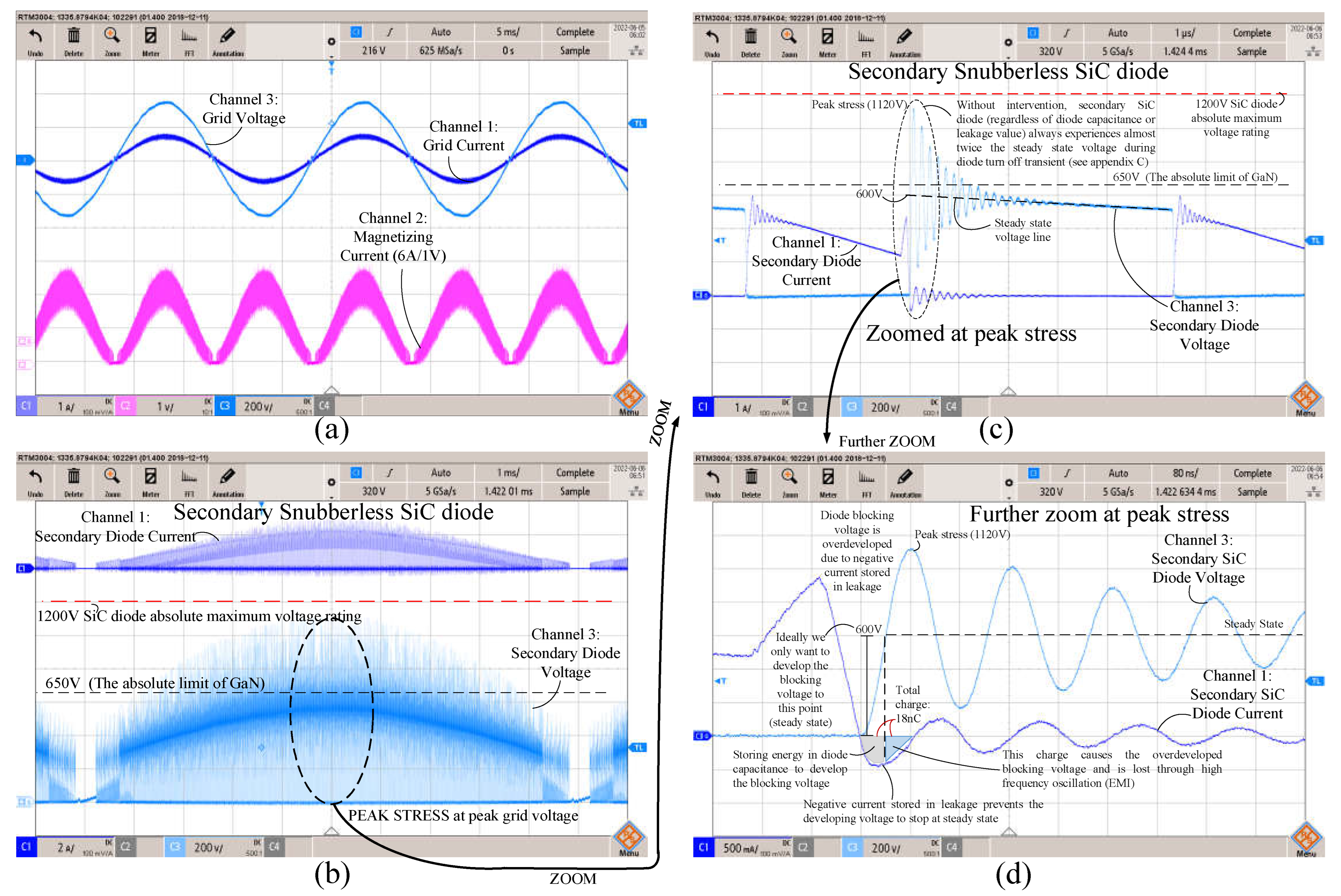
2. The Secondary Leakage—Rectifier Problem
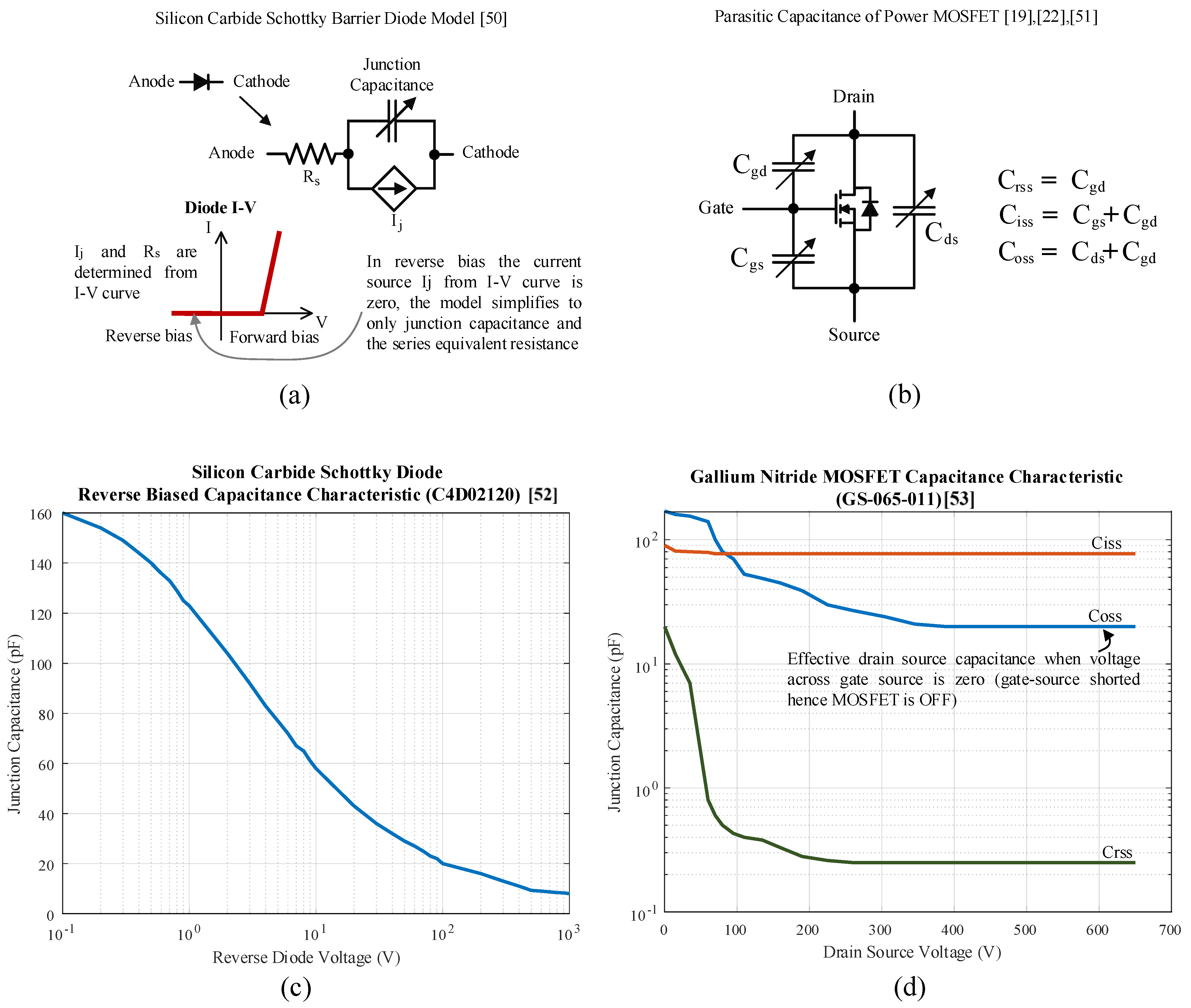
2.1. Problem with Using GaN as a Secondary Rectifier
2.2. Research Motivation
2.3. Previous Solution in the Literature
2.4. Scope of Study
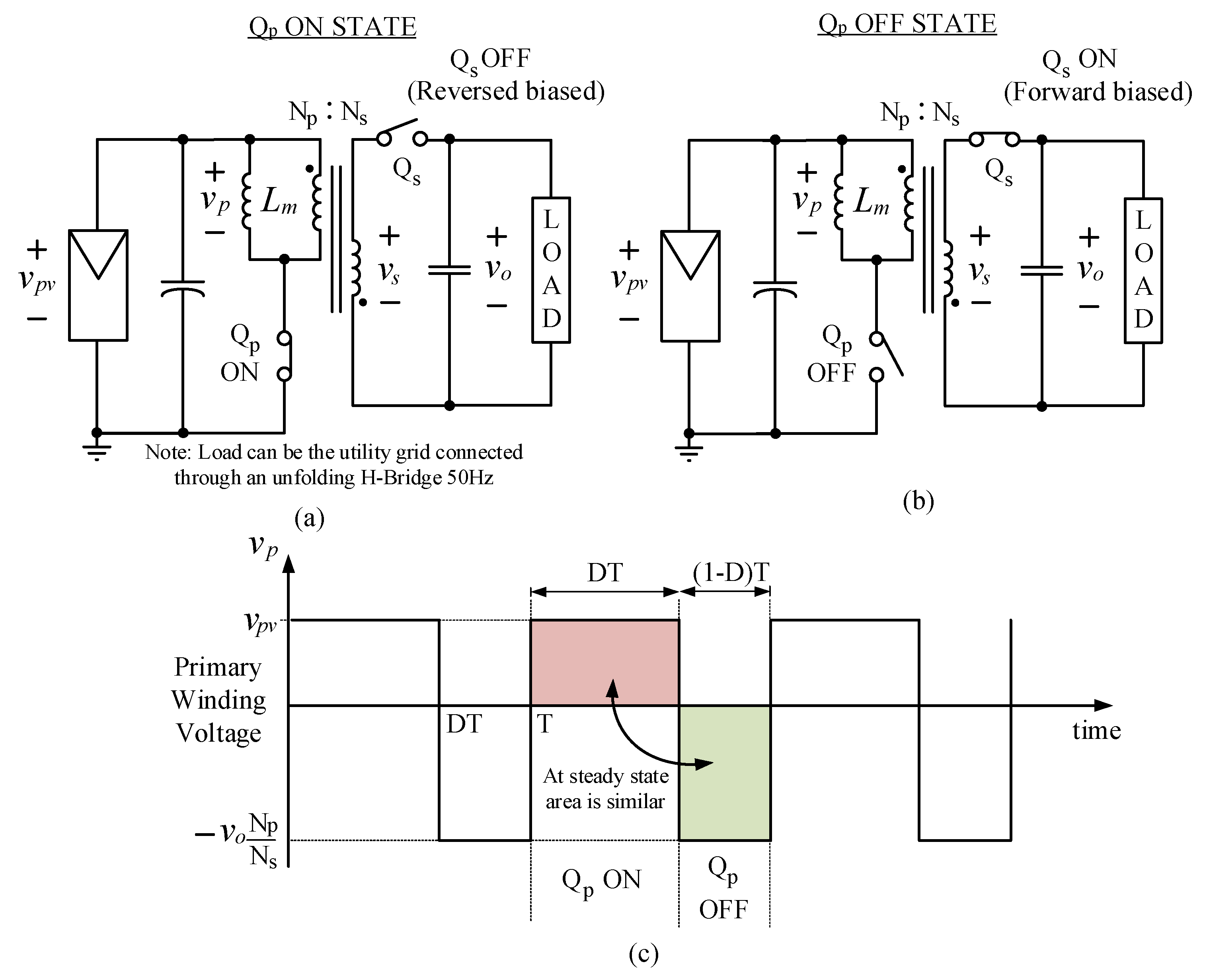
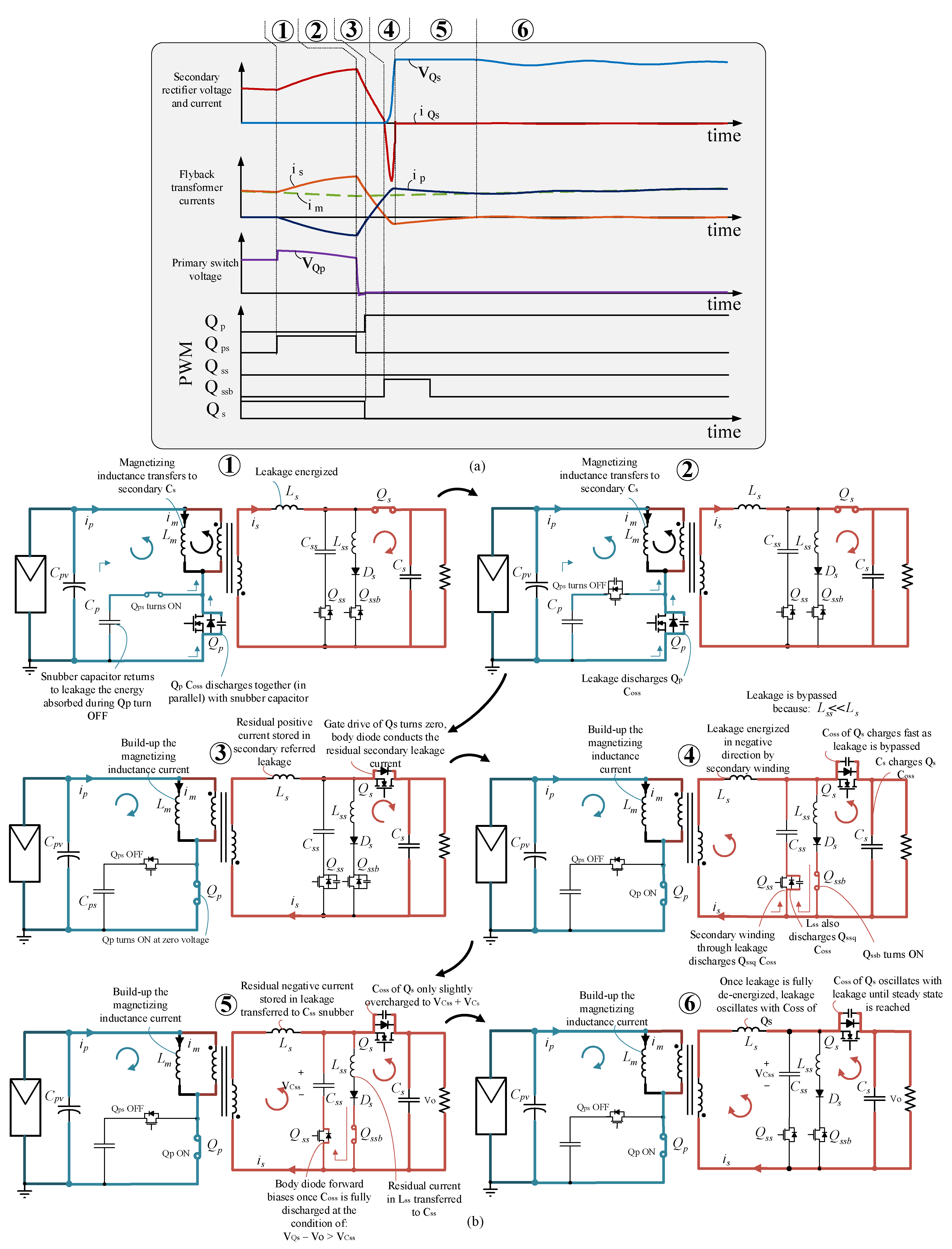
3. Principle
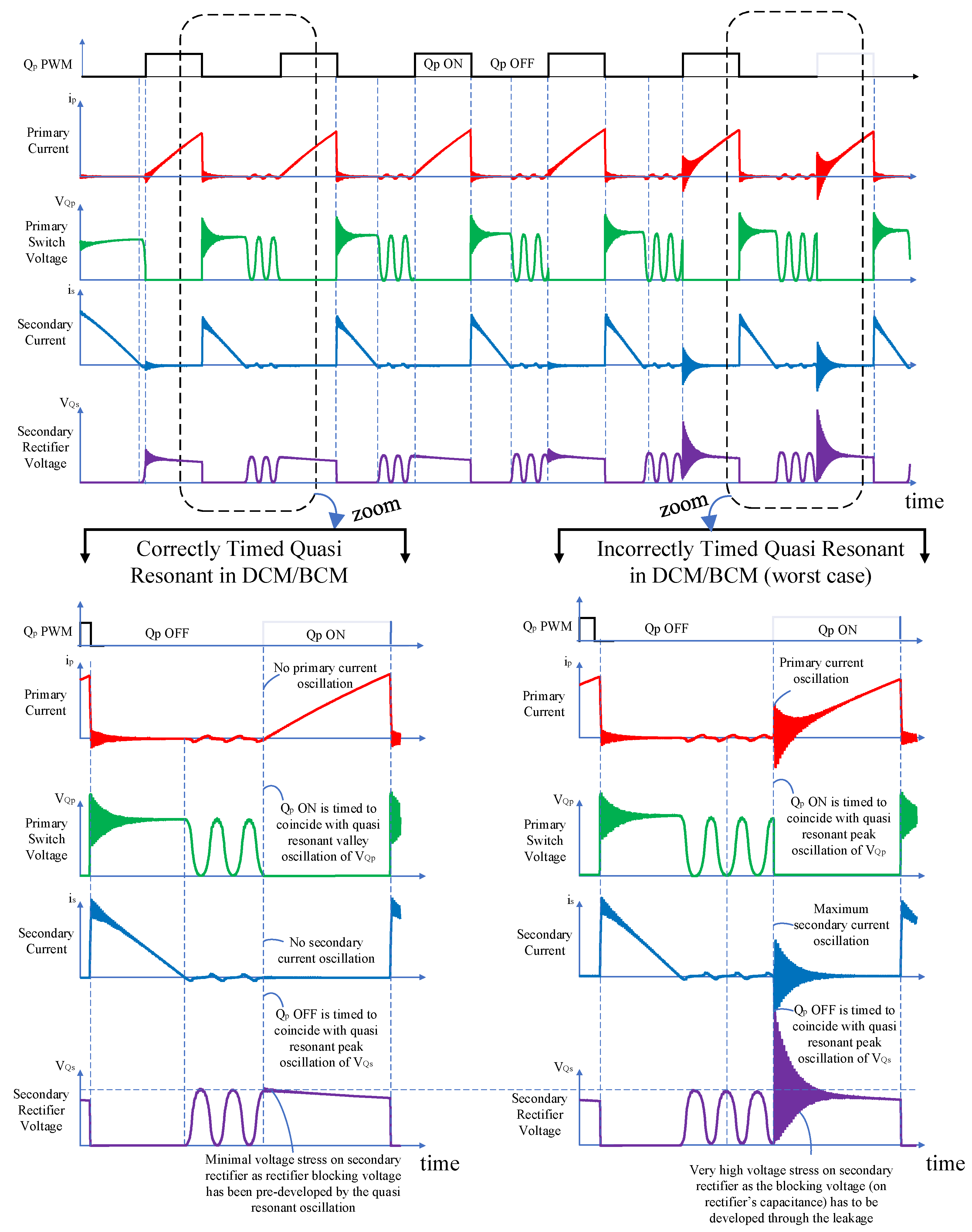
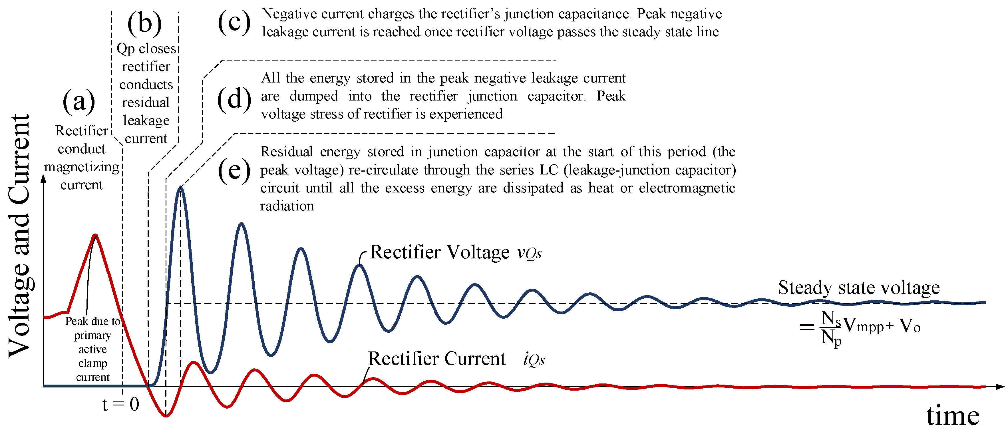
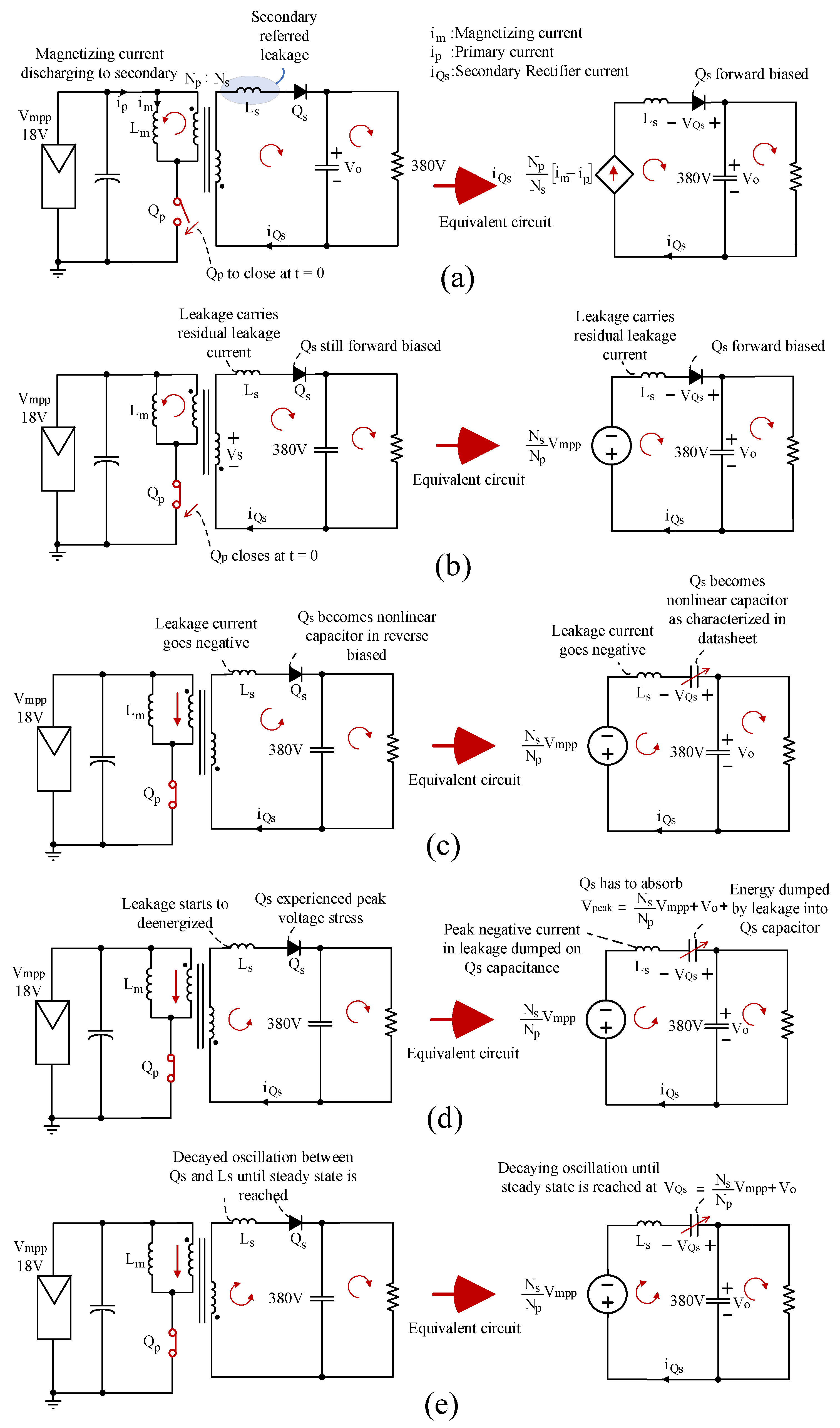
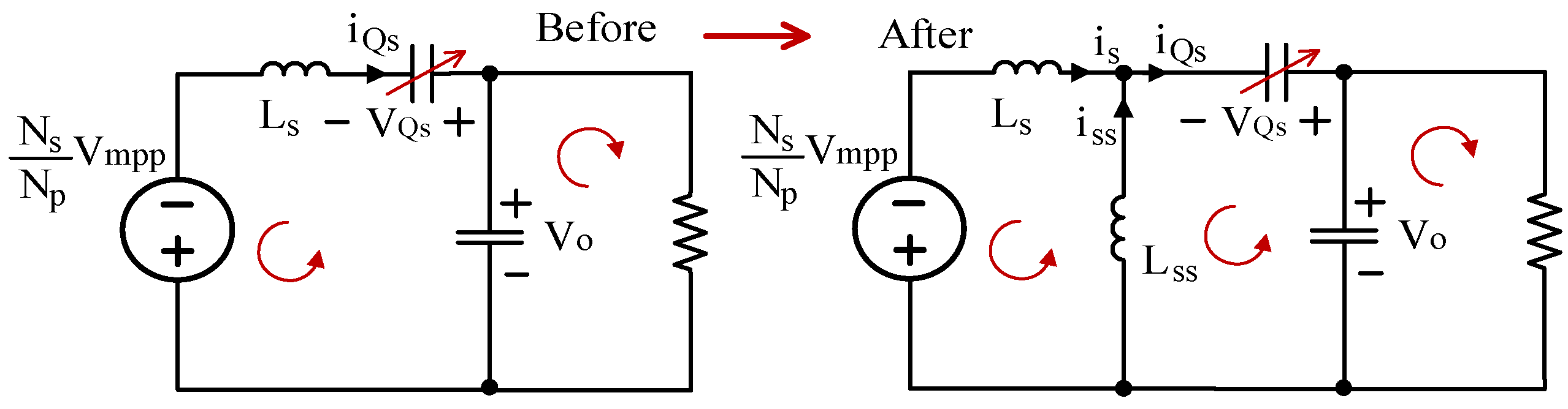
3.1. Theory of the Problem
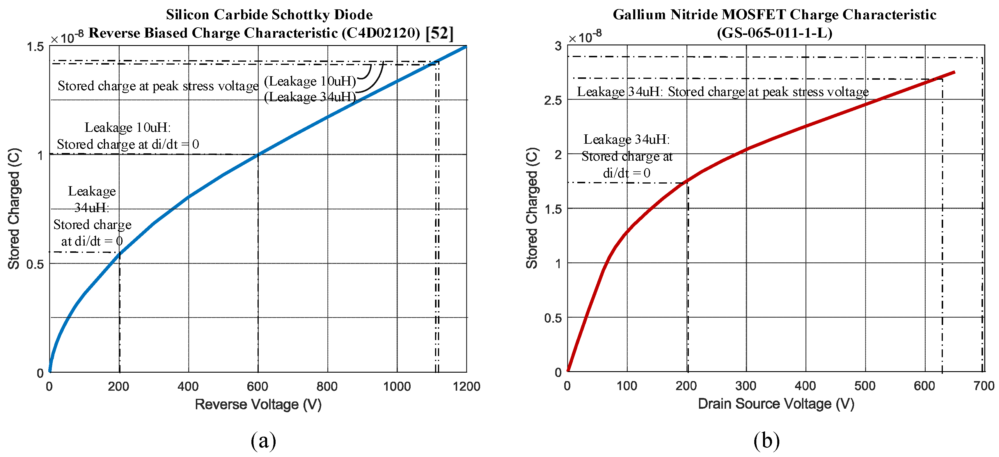
3.2. For Large Leakages
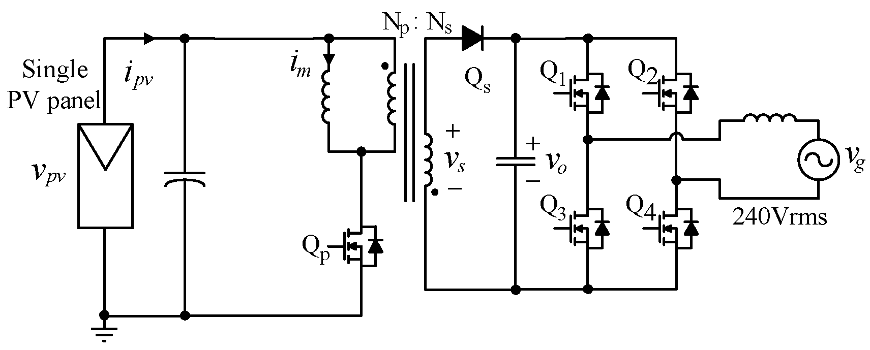
4. Proposed Solution: The Leakage Bypass

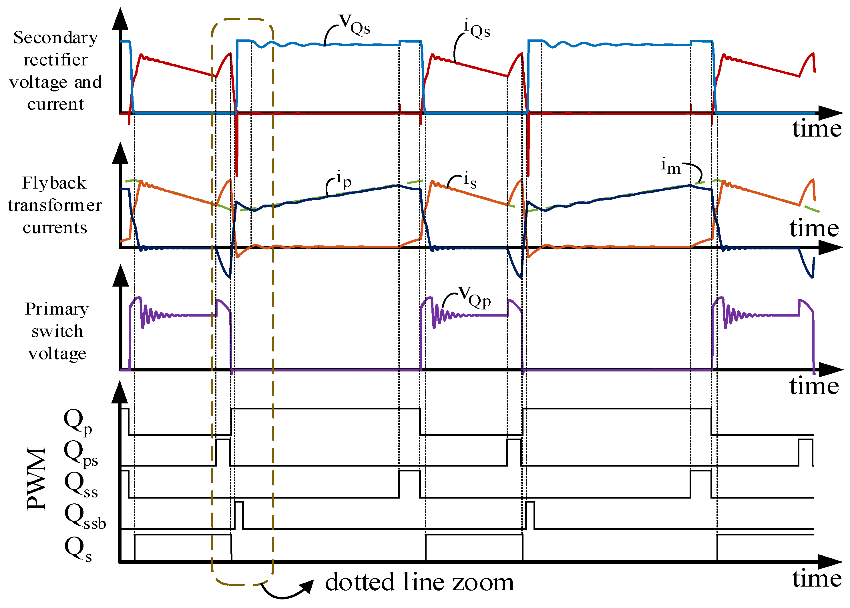
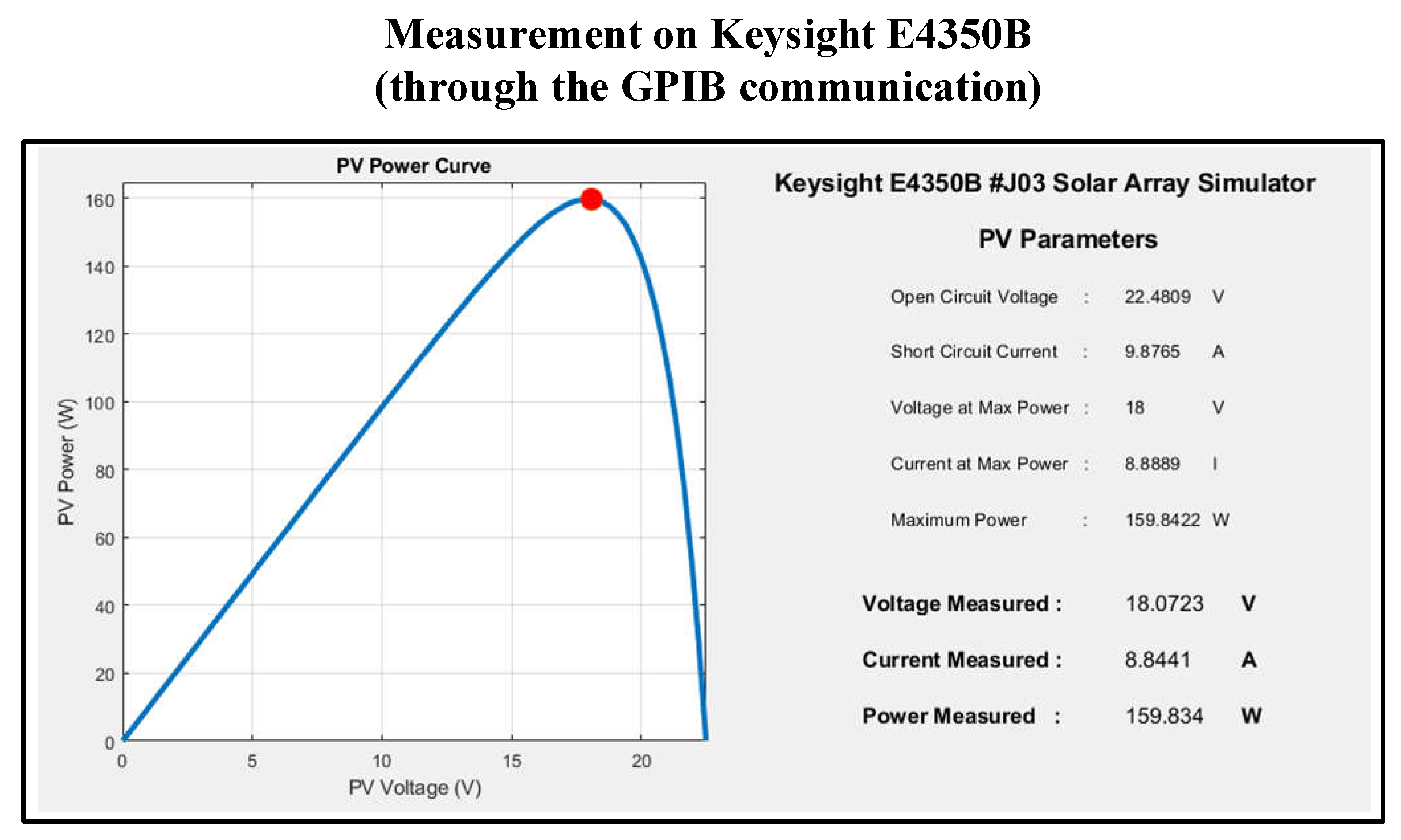
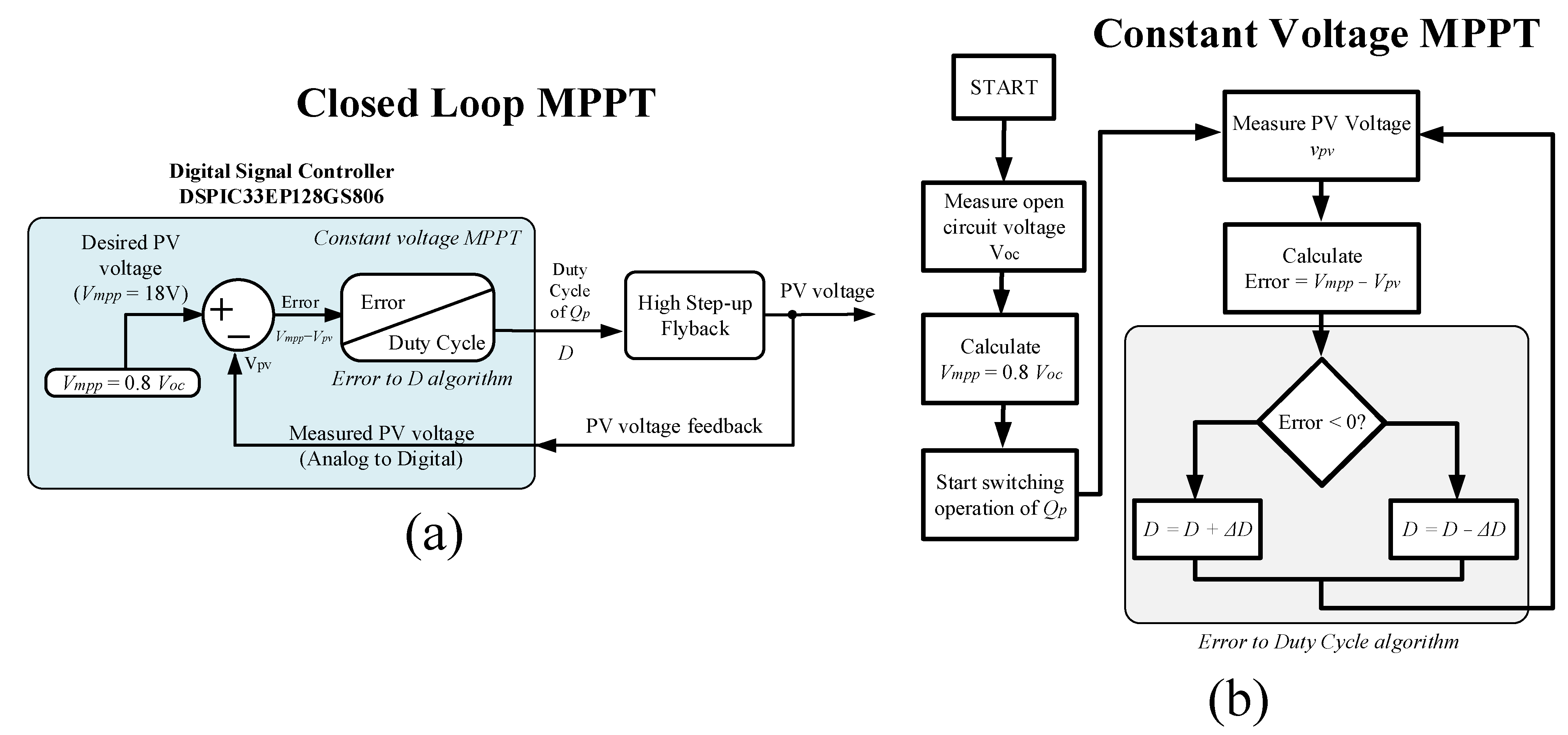
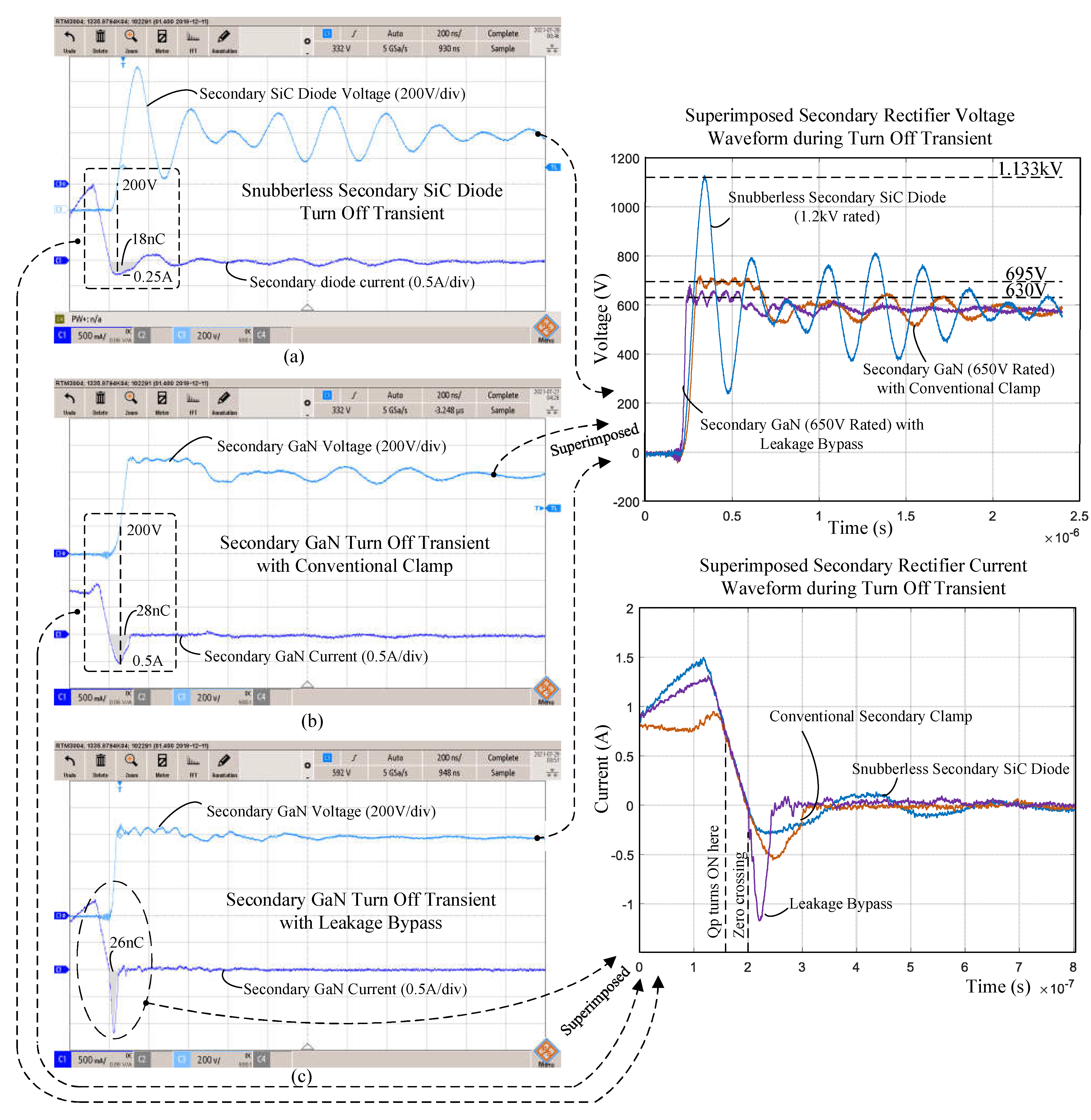
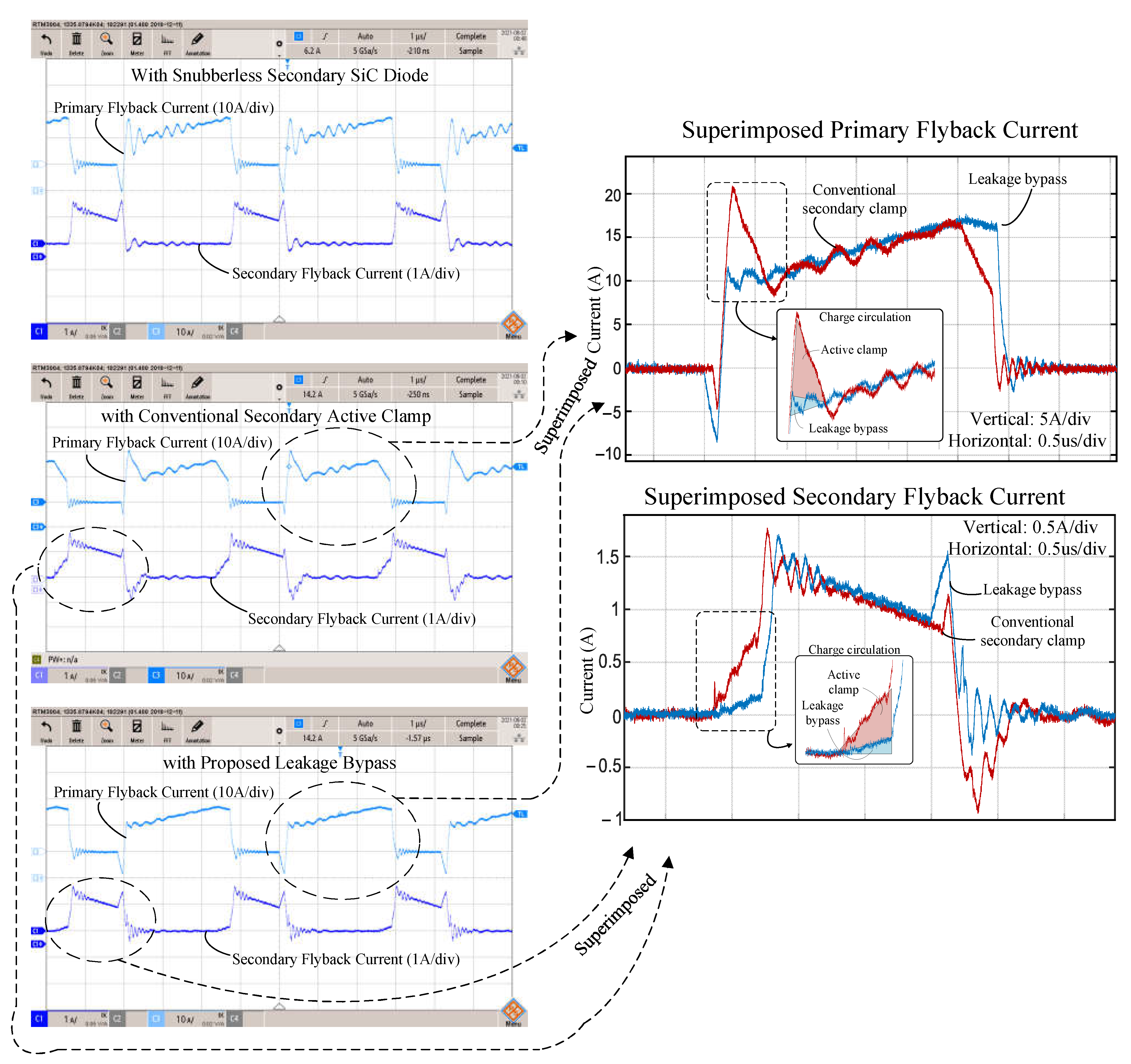
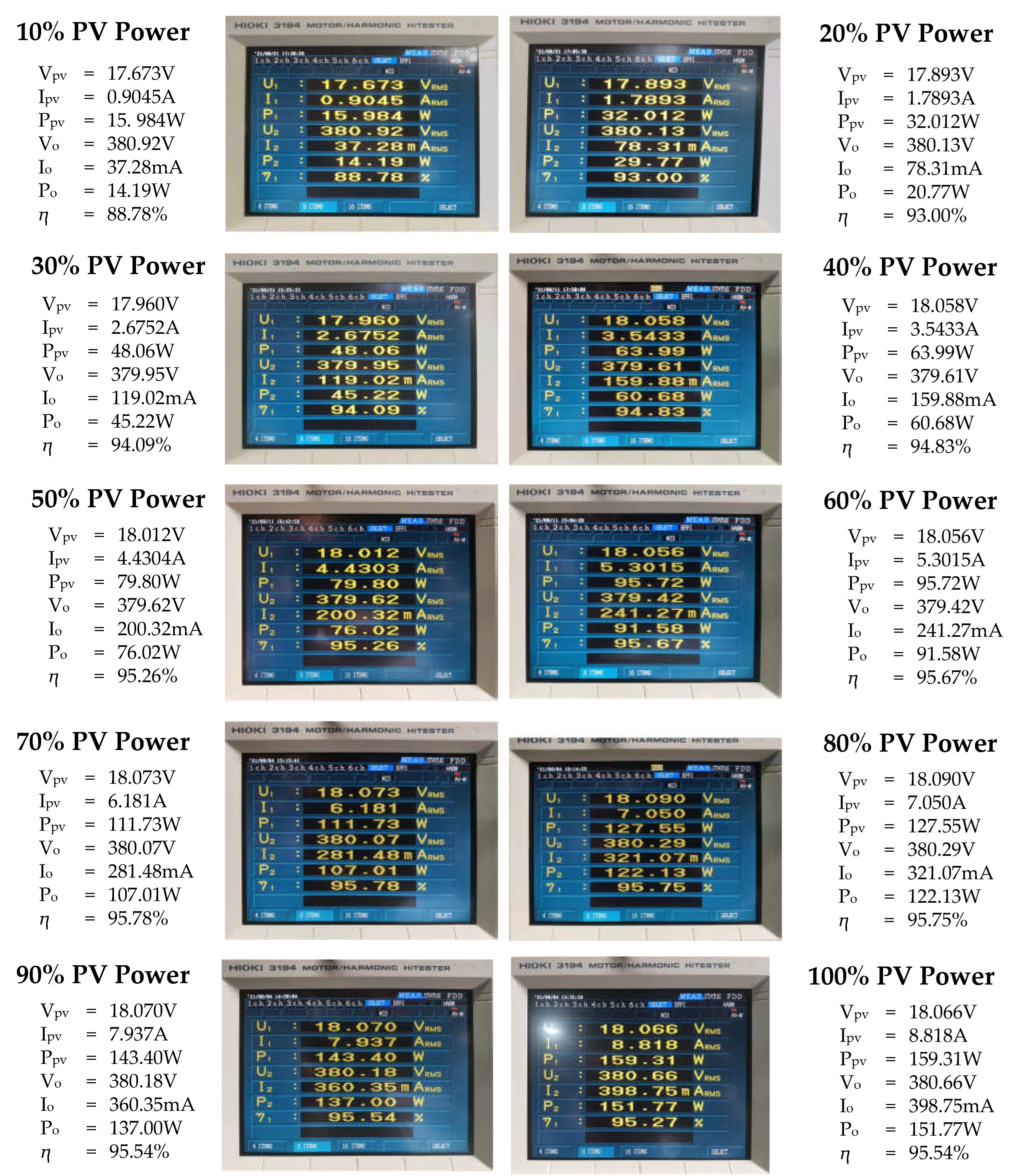
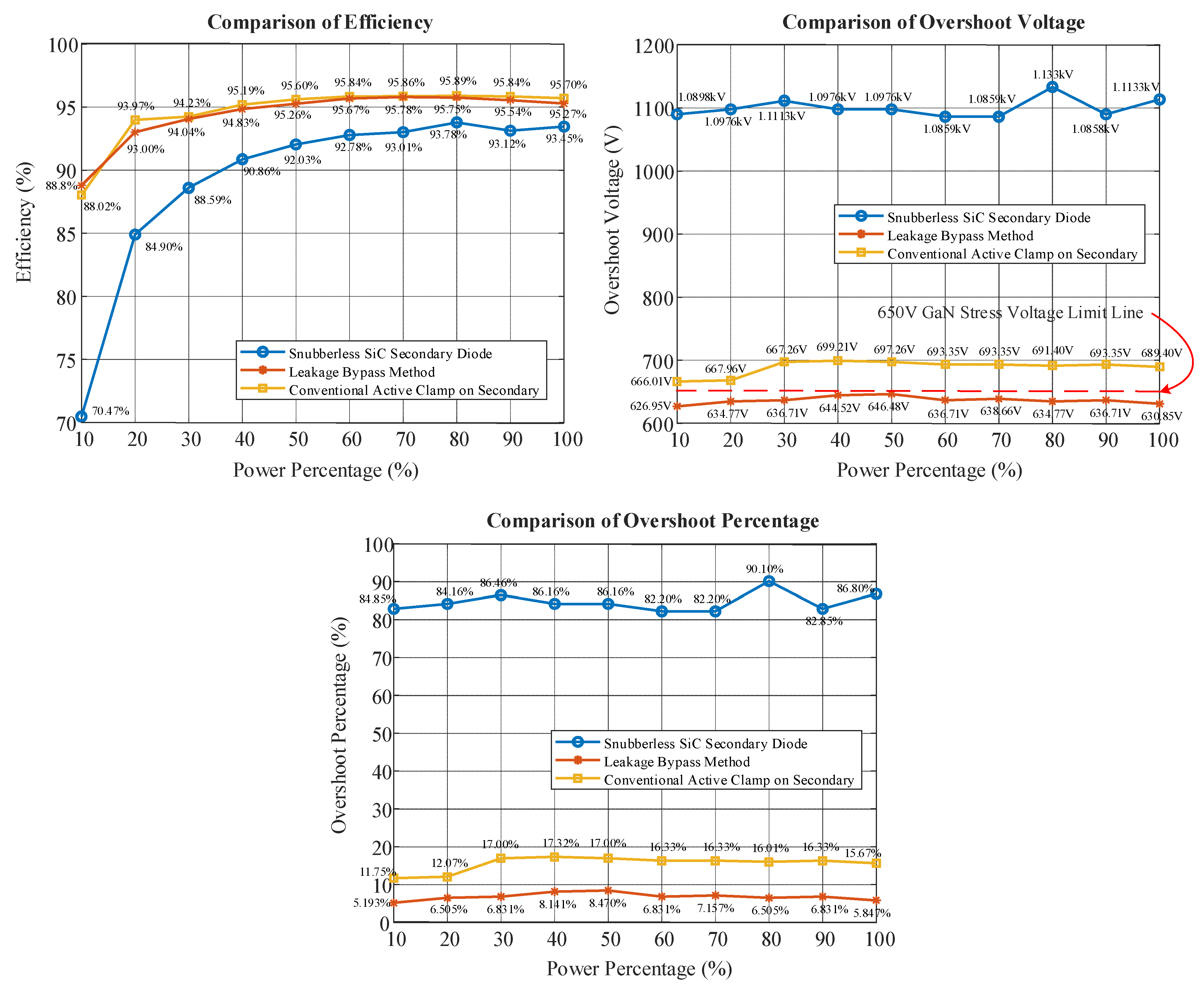
5. Experimental Results
6. Conclusions
Author Contributions
Funding
Institutional Review Board Statement
Informed Consent Statement
Data Availability Statement
Acknowledgments
Conflicts of Interest
Nomenclature
| Symbol | Description | Symbol | Description |
| 2DEG | Two-dimensional Electron Gas | MIT | Massachusetts Institute of Technology |
| BCM | Boundary Conduction Mode | MPPT | Maximum power point tracker |
| C | Capacitor | Np | Primary winding number of turns |
| CCM | Continuous Conduction Mode | Ns | Secondary winding number of turns |
| Cds | MOSFET drain source capacitance | PC | Personal computer |
| Cgd | MOSFET gate drain capacitance | PCB | Printed circuit board |
| Cgs | MOSFET gate source capacitance | Pmpp | Peak power point |
| Ciss | MOSFET input capacitance | PV | Photovoltaic |
| Coss | MOSFET output capacitance | Q | General charge |
| Cpv | Capacitor placed in parallel to PV input | Q1 | Unfolding H-Bridge MOSFET |
| CQs | Capacitance of rectifier (in GaN CQs = Coss) | Q2 | Unfolding H-Bridge MOSFET |
| Crss | MOSFET effective gate drain capacitance | Q3 | Unfolding H-Bridge MOSFET |
| Cs | Output capacitor of flyback | Q4 | Unfolding H-Bridge MOSFET |
| Css | Secondary clamp capacitor | Qm | Charge voltage at vss (when di/dt = 0) |
| D | Duty cycle of primary switch Qp | Qp | Primary flyback switch |
| DCM | Discontinous conduction mode | Qpeak | Peak charge stored in capacitor |
| Ds | Bypass diode | Qps | Primary flyback clamp switch |
| E | General energy stored in capacitor | Qs | Secondary flyback rectifier switch |
| Ec | Energy of capacitor in LC circuit (when di/dt = 0) | Qss | Secondary flyback clamp switch |
| EL | Energy of inductor in LC circuit (when di/dt = 0) | Qssb | Secondary flyback bypass switch |
| EMI | Electromagnetic inteference | Qv | General charge stored in rectifier |
| Epeak | Peak energy stored in capacitor in LC circuit | R | Resistance in LC circuit |
| fc | Resonance frequency of series LC circuit | Rds | Drain-source resistance of MOSFET |
| GaN | Gallium nitride | RF | Radio frequency |
| GPIB | General Purpose Interface Bus | RHP | Right half plane |
| HEMT | High Electron Mobility Transistor | RLC | Resistor-inductor-capacitor circuit |
| Ij | Current source in SiC diode model | Rm | Core resistance (to represent core loss) |
| IL | Current in LC circuit in function of time | Rp | Transformer primary winding resistance |
| im | Magnetizing current | Rs | Transformer secondary winding resistance |
| ip | Primary current | SiC | Silicon Carbide |
| ipeak | Peak current in secondary rectifier | T | Period |
| ipv | PV current | USB | Universal Serial Bus |
| iQs | Current of secondary rectifier | Vdss | MOSFET drain source max. voltage rating |
| is | Secondary current | vg | Grid voltage |
| KVL | Kirchoff voltage loop | Vmpp | Maximum power point voltage |
| L | Inductor in LC circuit | vo | Output voltage |
| LC | Inductor-capacitor | Voc | Open circuit voltage of PV |
| Lm | Magnetizing inductance | vp | Primary winding voltage |
| Lp | Primary referred leakage | vpeak | Peak voltage stress of rectifier |
| Ls | Secondary referred leakage | Vpeak | General peak voltage |
| Lss | Bypass inductor | vss | Voltage at steady state |
| vpv | PV voltage | ΔD | Increment of duty cycle in MPPT |
| vQp | Voltage across Qp | Δi | Peak rectifier current |
| vQs | Voltage across Qs | Δtm | Time to reach peak current from zero crossing |
| Vrms | Root mean squared voltage | ω | Frequency in radian |
| vs | Secondary winding voltage |
Appendix A. Derivation of Equation (1)
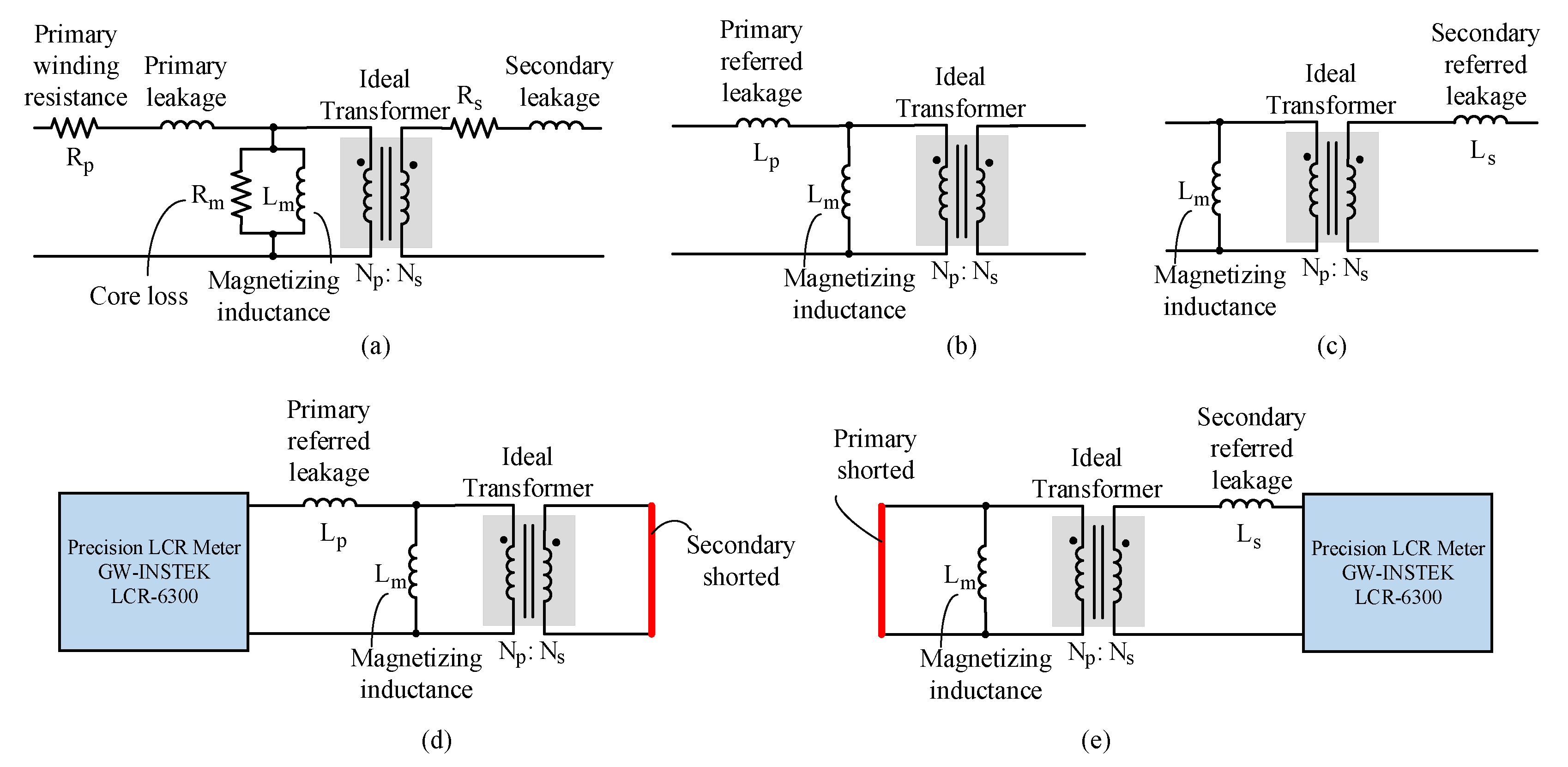
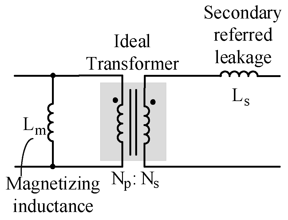
Appendix B. The Leakage of the Transformer
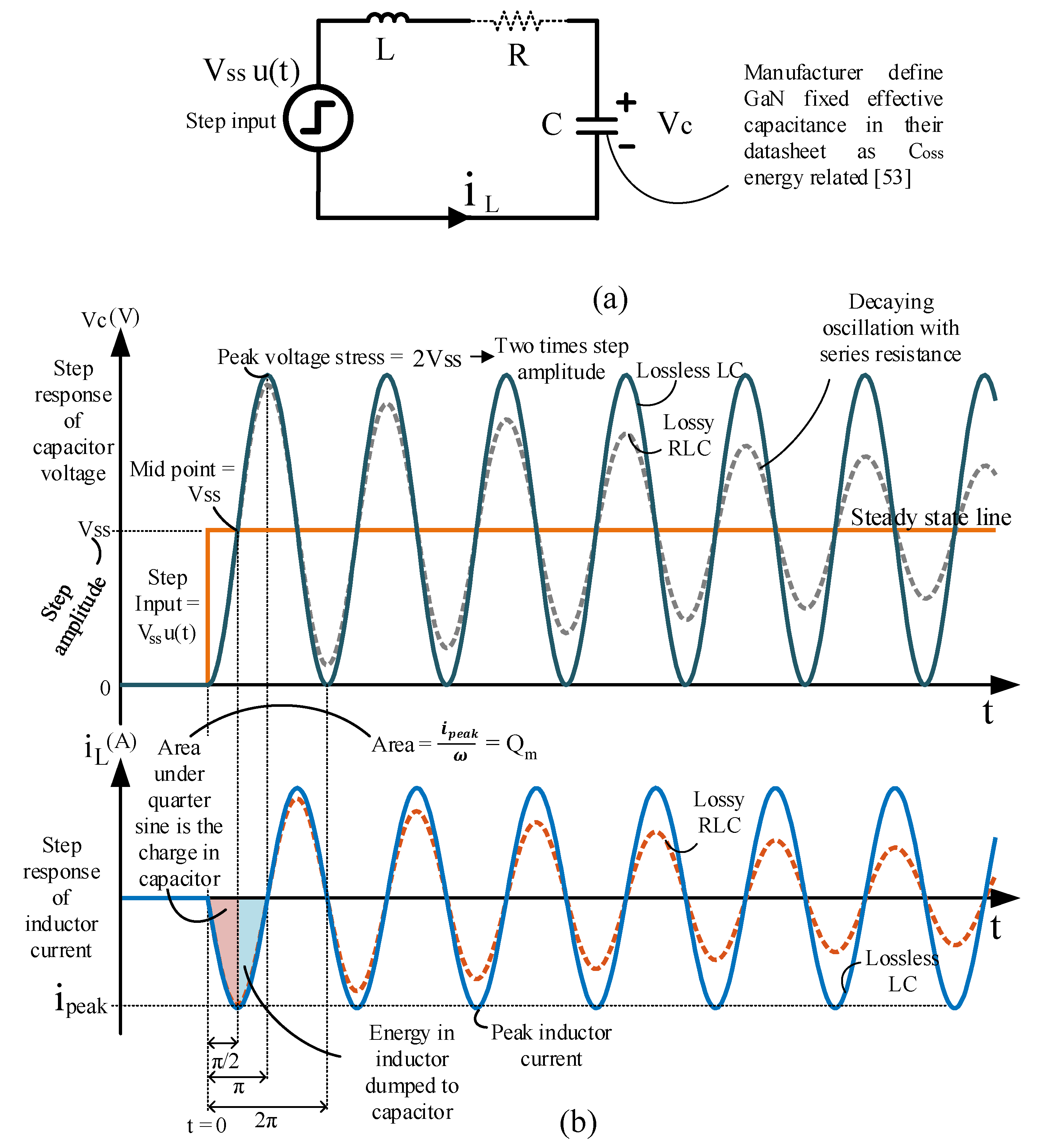
Appendix C. Correlation of the Problem to Series Lossless LC Resonant Circuit
Appendix D. Derivation of Equations (4), (5) and (8)

References
- Shimizu, T.; Wada, K.; Nakamura, N. Flyback-Type Single-Phase Utility Interactive Inverter with Power Pulsation Decoupling on the DC Input for an AC Photovoltaic Module System. IEEE Trans. Power Electron. 2006, 21, 1264–1272. [Google Scholar] [CrossRef]
- Koizumi, H.; Mizuno, T.; Kaito, T.; Noda, Y.; Goshima, N.; Kawasaki, M.; Nagasaka, K.; Kurokawa, K. A Novel Microcontroller for Grid-Connected Photovoltaic Systems. IEEE Trans. Ind. Electron. 2006, 53, 1889–1897. [Google Scholar] [CrossRef]
- Kyritsis, A.C.; Tatakis, E.C.; Papanikolaou, N.P. Optimum Design of the Current-Source Flyback Inverter for Decentralized Grid-Connected Photovoltaic Systems. IEEE Trans. Energy Convers. 2008, 23, 281–293. [Google Scholar] [CrossRef]
- Kasa, N.; Iida, T.; Chen, L. Flyback Inverter Controlled by Sensorless Current MPPT for Photovoltaic Power System. IEEE Trans. Ind. Electron. 2005, 52, 1145–1152. [Google Scholar] [CrossRef]
- Tan, G.H.; Wang, J.Z.; Ji, Y.C. Soft-switching flyback inverter with enhanced power decoupling for photovoltaic applications. IET Electr. Power Appl. 2007, 1, 264–274. [Google Scholar] [CrossRef]
- Zhang, F.; Gong, C. A New Control Strategy of Single-Stage Flyback Inverter. IEEE Trans. Ind. Electron. 2009, 56, 3169–3173. [Google Scholar] [CrossRef]
- Kim, Y.-H.; Jang, J.-W.; Shin, S.-C.; Won, C.-Y. Weighted-Efficiency Enhancement Control for a Photovoltaic AC Module Interleaved Flyback Inverter Using a Synchronous Rectifier. IEEE Trans. Power Electron. 2014, 29, 6481–6493. [Google Scholar] [CrossRef]
- Zhang, Z.; He, X.-F.; Liu, Y.-F. An Optimal Control Method for Photovoltaic Grid-Tied-Interleaved Flyback Microinverters to Achieve High Efficiency in Wide Load Range. IEEE Trans. Power Electron. 2013, 28, 5074–5087. [Google Scholar] [CrossRef]
- Kim, Y.-H.; Ji, Y.-H.; Kim, J.-G.; Jung, Y.-C.; Won, C.-Y. A New Control Strategy for Improving Weighted Efficiency in Photovoltaic AC Module-Type Interleaved Flyback Inverters. IEEE Trans. Power Electron. 2013, 28, 2688–2699. [Google Scholar] [CrossRef]
- Tamyurek, B.; Kirimer, B. An Interleaved High-Power Flyback Inverter for Photovoltaic Applications. IEEE Trans. Power Electron. 2015, 30, 3228–3241. [Google Scholar] [CrossRef]
- Kim, H.; Lee, J.S.; Kim, M. Downsampled Iterative Learning Controller for Flyback CCM Inverter. IEEE Trans. Ind. Electron. 2018, 65, 510–520. [Google Scholar] [CrossRef]
- Solis-Cisneros, H.I.; Sevilla-Camacho, P.Y.; Robles-Ocampo, J.B.; Zuñiga-Reyes, M.A.; Rodríguez-Resendíz, J.; Muñiz-Soria, J.; Hernández-Gutiérrez, C.A. A dynamic reconfiguration method based on neuro-fuzzy control algorithm for partially shaded PV arrays. Sustain. Energy Technol. Assess. 2022, 52 Pt B, 102147. [Google Scholar] [CrossRef]
- Oswald, N.; Anthony, P.; McNeill, N.; Stark, B.H. An Experimental Investigation of the Tradeoff between Switching Losses and EMI Generation with Hard-Switched All-Si, Si-SiC, and All-SiC Device Combinations. IEEE Trans. Power Electron. 2014, 29, 2393–2407. [Google Scholar] [CrossRef]
- Walder, S.; Oswald, N.; Yuan, X. EMI generation characteristics of SiC diodes: Influence of reverse recovery characteristics. IEEE Trans. Power Electron. 2015, 30, 1131–1136. [Google Scholar] [CrossRef]
- Hefner, A.; Singh, R.; Lai, J.-S.; Berning, D.; Bouche, S.; Chapuy, C. SiC power diodes provide breakthrough performance for a wide range of applications. IEEE Trans. Power Electron. 2001, 16, 273–280. [Google Scholar] [CrossRef]
- Fu, R.; Grekov, A.E.; Peng, K.; Santi, E. Parameter Extraction Procedure for a Physics-Based Power SiC Schottky Diode Model. IEEE Trans. Ind. Appl. 2014, 50, 3558–3568. [Google Scholar] [CrossRef]
- Yin, S.; Gu, Y.; Tseng, K.J.; Li, J.; Dai, G.; Zhou, K. A Physics-Based Compact Model of SiC Junction Barrier Schottky Diode for Circuit Simulation. IEEE Trans. Electron Devices 2018, 65, 3095–3103. [Google Scholar] [CrossRef]
- Colino, S.L.; Beach, R.A. Fundamental of Gallium Nitride Power Transistor; Application Note AN002; EPC: El Segundo, CA, USA, 2020; p. 2. [Google Scholar]
- Yan, D.; Hang, L.; He, Y.; He, Z.; Zeng, P. An Accurate Switching Transient Analytical Model for GaN HEMT under the Influence of Nonlinear Parameters. Energies 2022, 15, 2966. [Google Scholar] [CrossRef]
- Sun, B. Does GaN Have a Body Diode? Understanding the Third Quadrant Operation of GaN; Application Report SNOAA36; Texas Instrument: Dallas, TX, USA, 2019; p. 2. [Google Scholar]
- Styles, J. (GaN System) Common misconceptions about the body diode. In Power & Energy Efficiency Handbook; Design World: Cleveland, OH, USA, 2019; pp. 12–17. [Google Scholar]
- Zhang, Y.; Sun, M.; Perozek, J.; Liu, Z.; Zubair, A.; Piedra, D.; Chowdhury, N.; Gao, X.; Shepard, K.; Palacios, T. Large Area 1.2 kV GaN Vertical Power FinFETs with a Record Switching Figure-of-Merit. IEEE Electron Device Lett. 2019, 40, 75–78. [Google Scholar] [CrossRef] [Green Version]
- Mohan, N.; Undeland, T.M.; Robbins, W.P. Power Electronics Converts, Applications and Design, 3rd ed.; Wiley: New York, NY, USA, 2003; pp. 53, 56, 516, 537. [Google Scholar]
- Shang, L.; Xu, B.; Ma, S.; Ouyang, H.; Shan, H.; Hao, X.; Han, B. Enhanced luminescence property of GaN-based LEDs with p-InGaN cap layer grown on p-GaN surface. Mater. Sci. Semicond. Process. 2022, 146, 106666. [Google Scholar] [CrossRef]
- Hu, Y.; Hernández-Gutiérrez, C.A.; Solís-Cisneros, H.; Santana, G.; Kudriatsev, Y.; Camas-Anzueto, J.; López-López, M. Blue luminescence origin and Mg acceptor saturation in highly doped zinc-blende GaN with Mg. J. Alloys Compd. 2021, 897, 163133. [Google Scholar] [CrossRef]
- Anwar, A.R.; Sajjad, M.T.; Johar, M.A.; Hernández-Gutiérrez, C.A.; Usman, M.; Łepkowski, S.P. Recent Progress in Micro-LED-Based Display Technologies. Laser Photonics Rev. 2022, 16, 2100427. [Google Scholar] [CrossRef]
- Sang, L. Diamond as the heat spreader for the thermal dissipation of GaN-based electronic devices. Funct. Diam. 2021, 1, 174–188. [Google Scholar] [CrossRef]
- Hernández-Gutiérrez, C.; Kudriavtsev, Y.; Cardona, D.; Hernández, A.; Camas-Anzueto, J. Optical, electrical, and chemical characterization of nanostructured InxGa1-xN formed by high fluence In+ ion implantation into GaN. Opt. Mater. 2021, 111, 110541. [Google Scholar] [CrossRef]
- Hernández-Gutiérrez, C.A.; Casallas-Moreno, Y.L.; Cardona, D.; Kudriavtsev, Y.; Santana-Rodríguez, G.; Mendoza-Pérez, R.; Contreras-Puente, G.; Mendez-Garcia, V.H.; Gallardo-Hernández, S.; Quevedo-Lopez, M.A.; et al. Characterization of n-GaN/p-GaAs NP heterojunctions. Superlattices Microstruct. 2019, 136, 106298. [Google Scholar] [CrossRef]
- Mohammadi, M.; Adib, E. Lossless passive snubber for half bridge interleaved flyback converter. IET Power Electron. 2014, 7, 1475–1481. [Google Scholar] [CrossRef]
- Soltanzadeh, K.; Yousefi, M.R. Analysis and design of two-switch flyback converter with double passive lossless snubber. IET Power Electron. 2018, 11, 1187–1194. [Google Scholar] [CrossRef]
- Soltanzadeh, K.; Khalilian, H.; Dehghani, M. Analysis, design, and implementation of a zero voltage switching two-switch CCM flyback converter. IET Circuits Devices Syst. 2016, 10, 20–28. [Google Scholar] [CrossRef] [Green Version]
- Hsieh, Y.-C.; Chen, M.-R.; Cheng, H.-L. An Interleaved Flyback Converter Featured with Zero-Voltage Transition. IEEE Trans. Power Electron. 2011, 26, 79–84. [Google Scholar] [CrossRef]
- Mohammadi, M.; Adib, E.; Farzanehfard, H. Lossless passive snubber for double ended flyback converter with passive clamp circuit. IET Power Electron. 2014, 7, 245–250. [Google Scholar] [CrossRef]
- Yanlin, L. Topology Studies and Control of Microinverters for Photovoltaic Applications. Ph.D. Thesis, National University of Singapore, Singapore, January 2003; p. 141. [Google Scholar]
- Zhang, Z.; Chen, M.; Chen, W.; Jiang, C.; Qian, Z. Analysis and Implementation of Phase Synchronization Control Strategies for BCM Interleaved Flyback Microinverters. IEEE Trans. Power Electron. 2014, 29, 5921–5932. [Google Scholar] [CrossRef]
- Spiazzi, G.; Mattavelli, P.; Costabeber, A. High Step-Up Ratio Flyback Converter with Active Clamp and Voltage Multiplier. IEEE Trans. Power Electron. 2011, 26, 3205–3214. [Google Scholar] [CrossRef]
- Kim, K.; Lee, S.; Cha, W.; Kwon, J.; Kwon, B. Bidirectional Single Power-Conversion DC–AC Converter with Noncomplementary Active-Clamp Circuits. IEEE Trans. Ind. Electron. 2016, 63, 4860–4867. [Google Scholar] [CrossRef]
- Vartak, C.; Abramovitz, A.; Smedley, K.M. Analysis and Design of Energy Regenerative Snubber for Transformer Isolated Converters. IEEE Trans. Power Electron. 2014, 29, 6030–6040. [Google Scholar] [CrossRef]
- Shitole, A.B.; Sathyan, S.; Suryawanshi, H.M.; Talapur, G.G.; Chaturvedi, P. Soft-Switched High Voltage Gain Boost-Integrated Flyback Converter Interfaced Single-Phase Grid-Tied Inverter for SPV Integration. IEEE Trans. Ind. Appl. 2018, 54, 482–493. [Google Scholar] [CrossRef]
- Rezaei, M.A.; Lee, K.J.; Huang, A.Q. A High-Efficiency Flyback Micro-inverter With a New Adaptive Snubber for Photovoltaic Applications. IEEE Trans. Power Electron. 2016, 31, 318–327. [Google Scholar] [CrossRef]
- Sukesh, N.; Pahlevaninezhad, M.; Jain, P.K. Analysis and Implementation of a Single-Stage Flyback PV Microinverter With Soft Switching. IEEE Trans. Ind. Electron. 2013, 61, 1819–1833. [Google Scholar] [CrossRef]
- Li, Y.; Oruganti, R. A Low Cost Flyback CCM Inverter for AC Module Application. IEEE Trans. Power Electron. 2011, 27, 1295–1303. [Google Scholar] [CrossRef]
- Lee, S.-H.; Cha, W.-J.; Kwon, B.-H.; Kim, M. Discrete-Time Repetitive Control of Flyback CCM Inverter for PV Power Applications. IEEE Trans. Ind. Electron. 2016, 63, 976–984. [Google Scholar] [CrossRef]
- Edwin, F.F.; Xiao, W.; Khadkikar, V. Dynamic Modeling and Control of Interleaved Flyback Module-Integrated Converter for PV Power Applications. IEEE Trans. Ind. Electron. 2014, 61, 1377–1388. [Google Scholar] [CrossRef]
- Kim, H.; Lee, J.S.; Lai, J.-S.; Kim, M. Iterative Learning Controller with Multiple Phase-Lead Compensation for Dual-Mode Flyback Inverter. IEEE Trans. Power Electron. 2017, 32, 6468–6480. [Google Scholar] [CrossRef]
- Kim, S.; Lee, S.H.; Lee, J.S.; Kim, M. Dual-mode flyback inverters in grid-connected photovoltaic systems. IET Renew. Power Gener. 2016, 10, 1402–1412. [Google Scholar] [CrossRef]
- Kim, H.; Kim, M. Duty-ratio feedforward controller design for single-stage flyback CCM inverter. Electron. Lett. 2016, 52, 2053–2055. [Google Scholar] [CrossRef]
- Za’Im, R.; Jamaludin, J.; Rahim, N.A. Photovoltaic Flyback Microinverter with Tertiary Winding Current Sensing. IEEE Trans. Power Electron. 2019, 34, 7588–7602. [Google Scholar] [CrossRef]
- Funaki, T.; Kimoto, T.; Hikihara, T. Evaluation of High Frequency Switching Capability of SiC Schottky Barrier Diode, Based on Junction Capacitance Model. IEEE Trans. Power Electron. 2008, 23, 2602–2611. [Google Scholar] [CrossRef] [Green Version]
- Chen, K.; Zhao, Z.; Yuan, L.; Lu, T.; He, F. The Impact of Nonlinear Junction Capacitance on Switching Transient and Its Modeling for SiC MOSFET. IEEE Trans. Electron. Devices 2015, 62, 333–338. [Google Scholar] [CrossRef]
- Cree. C4D02120A Silicon Carbide Schottky Diode Datasheet; Cree: Scarborough, ON, Canada, 2016; p. 3. [Google Scholar]
- GaN Systems Inc. GS-065-011-1-L. Bottom-SideCcooled 650 V E-Mode GaN Transistor; Gan Systems: Kanata, ON, Canada, 2020; Volume 5, p. 200423. [Google Scholar]
- Sze, S.M. Semiconductor Devices Physics and Technology, 2nd ed.; Wiley: New York, NY, USA, 2002; p. 100. [Google Scholar]


| Manufacturer Part Number | Manufacturer | Drain Source Voltage (Vdss) | Drain Current | Rds On (Max) | Datasheet Year |
|---|---|---|---|---|---|
| GAN039-650NTBZ | Nexperia | 650 V | 60 A | 33 mΩ | 2021 |
| GAN041-650WSBQ | Nexperia | 650 V | 47.2 A | 41 mΩ | 2021 |
| GAN063-650WSAQ | Nexperia | 650 V | 34.5 A | 60 mΩ | 2020 |
| GS-065-004-1-L | GaN Systems | 650 V | 3.5 A | 500 mΩ | 2020 |
| GS-065-008-1-L | GaN Systems | 650 V | 8 A | 225 mΩ | 2020 |
| GS-065-011-1-L | GaN Systems | 650 V | 11 A | 150 mΩ | 2020 |
| GS-065-030-2-L-TR | GaN Systems | 650 V | 30 A | 50 mΩ | 2021 |
| GS66502B-MR | GaN Systems | 650 V | 7.5 A | 260 mΩ | 2020 |
| GS66504B-MR | GaN Systems | 650 V | 15 A | 130 mΩ | 2016 |
| GS66506T-MR | GaN Systems | 650 V | 22.5 A | 90 mΩ | 2020 |
| GS66508B-MR | GaN Systems | 650 V | 30 A | 63 mΩ | 2019 |
| GS66516B-MR | GaN Systems | 650 V | 60 A | 32 mΩ | 2018 |
| IGLD60R070D1AUMA3 | Infineon | 600 V | 15 A | 70 mΩ | 2021 |
| IGLD60R190D1AUMA1 | Infineon | 600 V | 10 A | 190 mΩ | 2021 |
| IGT40R070D1ATMA1 | Infineon | 400 V | 31 A | 70 mΩ | 2021 |
| IGT60R070D1ATMA4 | Infineon | 600 V | 31 A | 70 mΩ | 2021 |
| IGT60R190D1SATMA1 | Infineon | 600 V | 12.5 A | 190 mΩ | 2020 |
| NTP8G202NG | Onsemi | 600 V | 9 A | 350 mΩ | 2015 |
| NTP8G206NG | Onsemi | 600 V | 17 A | 180 mΩ | 2015 |
| P1H06300D8 | PNJSemi | 650 V | 10 A | 300 mΩ | 2020 |
| TP65H015G5WS | Transphorm | 650 V | 95 A | 18 mΩ | 2021 |
| TP65H035G4WS | Transphorm | 650 V | 46.5 A | 41 mΩ | 2021 |
| TP65H050G4BS | Transphorm | 650 V | 34 A | 60 mΩ | 2021 |
| TP65H070LSG-TR | Transphorm | 650 V | 25 A | 85 mΩ | 2021 |
| TP65H150G4LSG | Transphorm | 650 V | 13 A | 180 mΩ | 2021 |
| TP65H300G4LSG | Transphorm | 650 V | 6.5 A | 312 mΩ | 2022 |
| TP65H480G4JSG-TR | Transphorm | 650 V | 3.6 A | 560 mΩ | 2021 |
| TP90H050WS | Transphorm | 900 V * | 34 A | 63 mΩ | 2020 |
| TP90H180PS | Transphorm | 900 V * | 15 A | 205 mΩ | 2021 |
| TPH3202LD | Transphorm | 600 V | 9 A | 350 mΩ | 2018 |
| TPH3205WSB | Transphorm | 650 V | 36 A | 60 mΩ | 2018 |
| TPH3206LD | Transphorm | 600 V | 17 A | 180 mΩ | 2018 |
| TPH3207WS | Transphorm | 650 V | 50 A | 41 mΩ | 2018 |
| TPH3208LD | Transphorm | 650 V | 20 A | 130 mΩ | 2018 |
| TPH3212PS | Transphorm | 650 V | 27 A | 72 mΩ | 2017 |
| XGP6508B | Xinguan Tech. | 650V | 21 A | 150 mΩ | 2019 |
| Symbol | Quantity | Value |
|---|---|---|
| Vo | Output voltage | 380 V |
| Vpv | PV Input voltage | 18 V |
| Cs | Secondary filter capacitance | 330 nF |
| Cpv | PV capacitance | 2 mF |
| Cps | Primary clamp capacitor (C0G) | 94 nF |
| Css | Secondary clamp capacitor (C0G) | 94 nF |
| Lss | Secondary bypass inductor | 3.8 uH |
| Lm | Magnetizing inductance | 5.43 uH |
| Np | Primary winding (no. of turn) | 4 |
| Ns | Secondary winding (no. of turn) | 48 (ratio 1:12) |
| fsw | Nominal switching frequency | 240 kHz |
| Lp | Leakage (primary referred) | 0.3 uH |
| Ls | Leakage (secondary referred) | 34 uH |
| Symbol | Components | Part Number |
| Qp | Primary GaN switch | EPC2215 |
| - | Flyback transformer core | ETD34 |
| Qps | Primary active clamp GaN switch | EPC2012C |
| Qs | Secondary GAN Rectifier | GS-065-011-1-L |
| Qssb | Secondary bypass GaN switch | GS-065-004-1-L |
| Qss | Secondary snubber GaN switch | GS-065-004-1-L |
| Ds | Bypass SiC diode | C3D1P7060Q |
| Experimental Figure | Device | Series Leakage | Measured Peak Stress Voltage vpeak | Measured Charge at vpeak | Datasheet’s charge at vpeak |
|---|---|---|---|---|---|
| Figure 2d | C4D02120A (SiC) | 10 uH | 1120 V | 18 nC | 14 nC |
| Figure 17a | C4D02120A (SiC) | 34 uH | 1133 V | 18 nC | 14 nC |
| Figure 17b | GS-065-011-1-L (GaN) | 34 uH | 695 V | 28 nC | 29 nC |
| Figure 17c | GS-065-011-1-L (GaN) | 34 uH | 630 V | 26 nC | 27 nC |
| Primary Charge | Secondary Charge | |
|---|---|---|
| Conventional Clamp | 2071.7 nC | 126.95 nC |
| Leakage Bypass | 443.68 nC | 31.24 nC |
| Reduction | 4.67 times smaller | 4.06 times smaller |
Publisher’s Note: MDPI stays neutral with regard to jurisdictional claims in published maps and institutional affiliations. |
© 2022 by the authors. Licensee MDPI, Basel, Switzerland. This article is an open access article distributed under the terms and conditions of the Creative Commons Attribution (CC BY) license (https://creativecommons.org/licenses/by/4.0/).
Share and Cite
Za’im, R.; Jamaludin, J.; Yusof, Y.; Rahim, N.A. High Step-Up Flyback with Low-Overshoot Voltage Stress on Secondary GaN Rectifier. Energies 2022, 15, 5092. https://doi.org/10.3390/en15145092
Za’im R, Jamaludin J, Yusof Y, Rahim NA. High Step-Up Flyback with Low-Overshoot Voltage Stress on Secondary GaN Rectifier. Energies. 2022; 15(14):5092. https://doi.org/10.3390/en15145092
Chicago/Turabian StyleZa’im, Radin, Jafferi Jamaludin, Yushaizad Yusof, and Nasrudin Abd Rahim. 2022. "High Step-Up Flyback with Low-Overshoot Voltage Stress on Secondary GaN Rectifier" Energies 15, no. 14: 5092. https://doi.org/10.3390/en15145092
APA StyleZa’im, R., Jamaludin, J., Yusof, Y., & Rahim, N. A. (2022). High Step-Up Flyback with Low-Overshoot Voltage Stress on Secondary GaN Rectifier. Energies, 15(14), 5092. https://doi.org/10.3390/en15145092