Article

A High-Power-Density Active-Clamp Converter with Integrated Planar Transformer

1
Department of Electrical Engineering, Inha University, Incheon 22212, Korea
2
Department of Electrical Engineering, Incheon National University, Incheon 22012, Korea
*
Author to whom correspondence should be addressed.
Energies 2022, 15(15), 5609; https://doi.org/10.3390/en15155609
Submission received: 28 June 2022 / Revised: 20 July 2022 / Accepted: 27 July 2022 / Published: 2 August 2022
(This article belongs to the Topic Advanced Electric Vehicle Technology)

Abstract

:
This paper proposes an active-clamp forward-flyback (ACFF) converter with an integrated planar transformer for wide-input voltage and high-output current applications, such as low-voltage direct-current (LDC) converters in electric vehicles. An integrated planar transformer that consists of a forward-flyback transformer, single primary winding, and efficient structure of secondary windings is adopted for the proposed converter, and since this transformer is implemented with a common four-layer printed circuit board (PCB) winding, a high power density and low cost of the proposed converter can be achieved. In addition, due to the low leakage inductance induced by the planar transformer, a reduced commutation period can be achieved, and it is possible to increase the switching frequency resulting in low volume of transformer. Although the integrated planar transformer has relatively high conduction loss, the active-clamp topology can significantly reduce the conduction loss on switches compared with widely used full-bridge (FB) converters because it only utilizes two switches and shows the low circulating current. As a result, the proposed converter with an integrated planar transformer has strengths in high power density and cost competitiveness without degraded efficiency, and it is a very attractive topology for LDC converters and other applications that require wide-input voltage and high-output current.

1. Introduction

Increasing demands for reducing CO2 emissions to comply with strict CO2 regulations have dramatically accelerated the development of the high fuel economy or zero CO2 emissions vehicles, such as hybrid and electric vehicles [1,2]. In accordance with this tendency, most vehicle manufacturers have recently invested trillions of dollars in research and development for electric vehicles [3]. These electric vehicles consist of various electrical power conversion systems since not only the conventional fossil-fuel engine and generator systems are replaced by motor, inverter, and low-voltage direct-current (LDC) converter, but also a high-voltage battery, on-board charger (OBC), or fuel-cell systems are used to substitute for the fuel tank [4,5]. This means that high-efficiency power conversion systems must be required to achieve a high fuel economy and extend the driving range. In addition, since these power conversion systems are installed in a limited space inside the vehicles and have a relatively high cost, achieving a high power density as well as being highly cost-competitive is a key design factor for power conversion systems in electric vehicles.
In the electric vehicle system, as shown in Figure 1, an LDC converter is applied not only to charge the low-voltage (LV) battery but also to provide power to electric devices, e.g., ignition (IG) systems, infotainment system, advanced driver assistance system (ADAS), autonomous driving system (ADS), traction control system (TCS), etc., by utilizing the high-voltage (HV) battery as an input source. In order to provide stable electrical power, the LDC is usually developed for 1.8 kW–2.4 kW/130–170 A output specifications. Moreover, LDC converters have to cover wide input and output voltage variations since both input and output consist of batteries. For instance, a hybrid electric vehicle (HEV) usually adopts a 150–350 V range HV battery, a plug-in hybrid electric vehicle (PHEV) uses a 200–400 V range HV battery, and a 200–400 V or 400–800 V HV battery is applied in an electric vehicle (EV). Moreover, although the nominal output voltage specification is 13.9 V, a 7–15.1 V output voltage range must be supported by the LDC converter to ensure stable operation under adverse conditions.
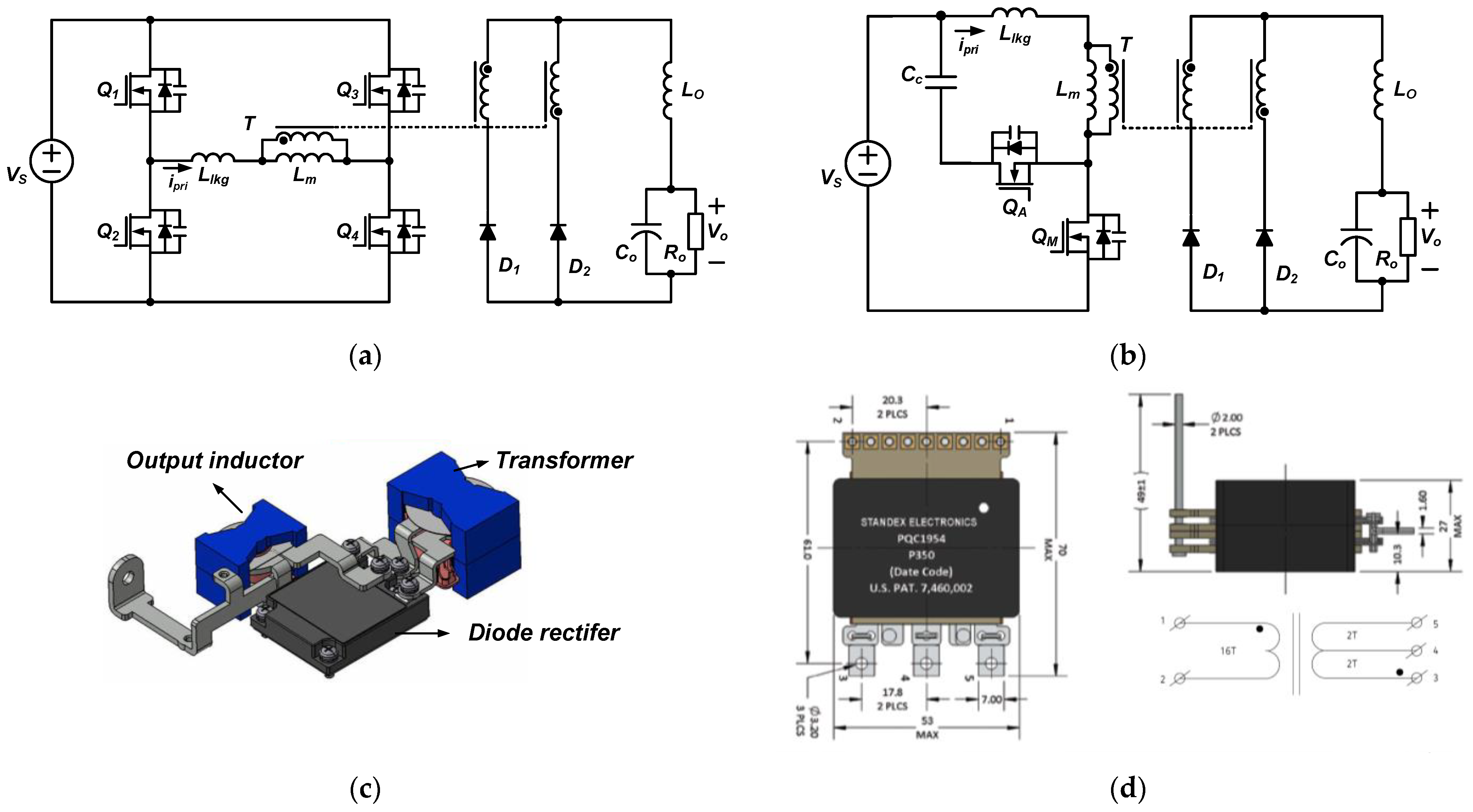
In general, in order to supply electrical power, the conventional phase-shifted full-bridge (PSFB) converter shown in Figure 2a has been widely applied to the LDC converter due to its ZVS characteristic and small output filter size. However, due to the wide input and output voltage specifications, the low nominal operating duty ratio of the PSFB converter causes an expansion of the freewheeling period and a large circulating current. Thus, the PSFB converter has trouble with high conduction loss. In addition, as shown in Figure 2c, the two magnetic components in conventional LDC converters require a complex structure. As a result, there are limitations to reducing the volume of the PSFB LDC converter. In order to compensate for drawbacks of the PSFB converter, many DC/DC converters have been studied for a low circulating current and a small volume of the magnetic components [6,7,8,9,10,11]. However, most of these converters still suffer from an increased volume and cost because of auxiliary components, such as additional switches, drive circuits, and additional inductors.
Besides PSFB converters, the conventional active-clamp forward (ACF) converter shown in Figure 2b is a promising candidate for LDC converters due to its low circulating current and low number of primary switches. However, the conventional ACF converter is also troubled with several disadvantages, such as high-voltage stress on switches and a complex secondary structure caused by the magnetic components. In order to restrain the high-voltage stress on switches, three-switch and three-level ACF converters that can utilize the common 600 V rating silicon (Si) metal–oxide–semiconductor field-effect transistor (MOSFET) are presented [12,13,14]. However, as the high-performance and high-voltage-rating silicon-carbide (SiC) MOSFET has been commercialized and mass-produced, the cost of the SiC MOSFET has gradually declined. As a result, the high price of the SiC MOSFET is no longer a drawback, so the SiC MOSFET has been rapidly applied to vehicle applications, replacing the Si MOSFET.
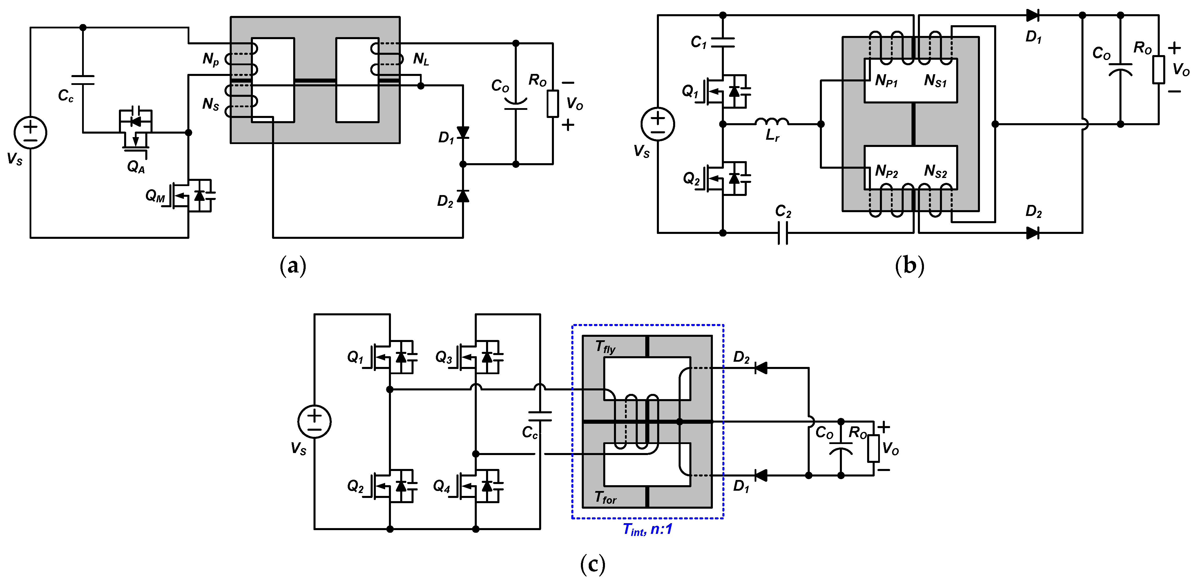
Contrary to the high-voltage stress on switches, the large volume and complex structure of the secondary side make it difficult to increase power density and cost competitiveness. Thus, to improve the power density and simplify the secondary side structure, ACF and active-clamp forward-flyback (ACFF) converters with an integrated transformer are proposed [15,16,17,18,19,20] as shown in Figure 3. However, despite the integrated transformer, such converters as shown in Figure 3a,b utilize a multi-winding structure that increases its complexity. Moreover, the windings of the integrated transformer in these converters are wound outside the core, making it vulnerable to electromagnetic interference (EMI). The full-bridge active-clamp forward-flyback (FBACFF) converter shown in Figure 3c complements theses drawbacks and shows a simple structure. The integrated transformer of this converter has a minimized winding number and turns as well as those that are wound inside the core. Meanwhile, it still uses the conventional winding method adopting litz wire and a busbar. In addition, the full-bridge structure of the primary side shows a relatively lower power density than the active-clamp structure, so it is hard to achieve a high power density, which is one of the most important design factors in vehicle applications.
In order to achieve high power density by reducing the volume of the magnetic component, various types of planar magnetics have been developed and sold on the market [21]. However, the conventional planar magnetics simply alternate enameled copper or litz wires to a complex multi-layer PCB winding and busbar, as shown in Figure 2d, so the cost of the planar magnetics is also expensive, and the secondary rectifier still shows a complex structure. Thus, planar magnetics have been rarely adopted for vehicle converters, and most manufacturers of vehicle converters still utilize a conventional winding transformer rather than adopting planar magnetics.
To maximize power density, high-frequency converters with a planar transformer, e.g., over 500 kHz, have been studied and researched [22,23]. These high-frequency converters are very susceptible to the parasitic components of the planar transformer, switch, and diode, so it is hard to ensure stable operation. In addition, provided that the resonant converter is applied to the high-frequency converter due to low switching loss, it is difficult for this converter to cover a wide input and output voltage range, and an auxiliary converter for output voltage regulation must be required, resulting in low power density and high cost. Furthermore, these converters utilize a high-cost multi-layer PCB for the planar transformer and a metal PCB for heat dissipation. Because of these limitations, conventional high-frequency converters with a planar transformer are not suitable for LDC converters that require cost competitiveness and high reliability.
To produce a highly competitive LDC converter, characteristics of high power density, low cost, and wide voltage range should be required, and in order to develop an attractive converter for manufacture, research should be conducted based on several research hypotheses as follows. (1) The active-clamp structure shows low conduction loss on primary switches and a high-power-density characteristic. (2) Planar magnetics can achieve a high power density, but it results in relatively high conduction loss. (3) To cover a wide input and output voltage range, utilizing two magnetic components, such as a transformer and output inductor, for isolation and output voltage regulation is recommended rather than adopting a single isolation transformer. (4) The integration of two magnetic components is possible by configuring and redesigning the windings and core structure, and it can result in a high power density.
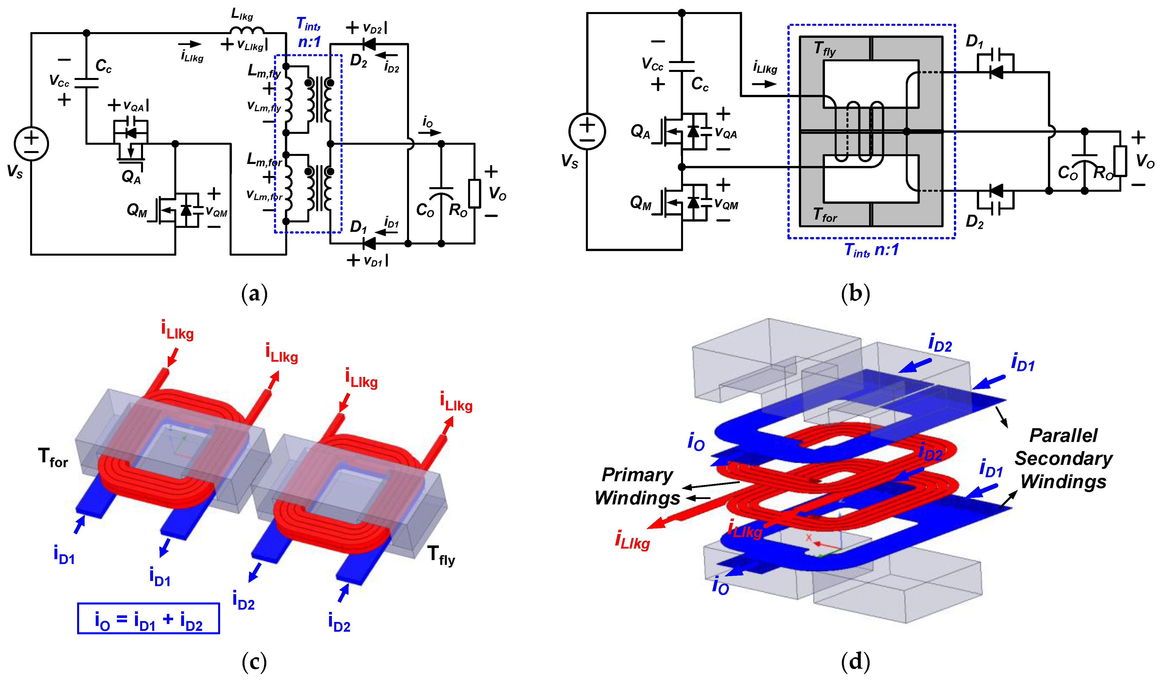
In this paper, considering the above-mentioned hypotheses, an ultrahigh-power-density ACFF converter with an integrated planar transformer for an LDC converter in an electric vehicle is presented, as shown in Figure 4. The proposed converter is derived from the conventional active-clamp forward-flyback converter, and only two SiC MOSFETs are used on the primary side of the converter, inducing a minimized volume on the primary side. In addition, the integrated planar transformer reduces the volume of the magnetics and provides a simple structure of the secondary rectifier by merging the forward and flyback transformers, as shown in Figure 4c, which are similar to the transformer and output inductor of conventional PWM converters. Moreover, although the power density of the converter is maximized by the PCB windings, the PCB winding of the integrated planar transformer, as shown in Figure 4d, can be implemented without any cost because it is composed of a commonly used 3Oz, four-layer PCB, which is used for the power stage of the converter. As a result, the proposed converter can achieve the advantages of both a high-frequency converter and a general PWM converter at the same time, such as a high power density, low cost, and wide input and output voltage range. Therefore, the proposed converter in this paper is a very valuable converter, especially in vehicle applications, since the strict requirements for vehicle applications can be satisfied by the proposed converter.
In order to support the effectiveness of the proposed converter, the detailed design procedure and design considerations are explained, and a prototype with 200–310 V input and 1.8 kW (13.9 V/130 A) output was constructed following the design procedure and considerations. Moreover, the experimental results compared with a conventional FBACFF converter are presented to verify the validity of the proposed LDC converter.

2. Features of the Proposed Converter

2.1. Descriptions of the Proposed Converter

The proposed converter is derived from the conventional active-clamp forward-flyback converter, and as presented in Figure 4, it shows a similar circuit diagram compared with the conventional one except for an integrated planar transformer. The integrated transformer of the proposed converter contains series-connected forward-flyback transformers based on [20], and it is implemented by utilizing two separate UI cores, as shown in Figure 4d. The windings of the integrated transformer are wound inside the cores, so not only low EMI noise but also an optimized PCB layout can be achieved. In addition, since the two UI cores of the integrated transformer share the primary winding, the applied voltage on the magnetizing inductance of each core is much less than that of the conventional converters, e.g., PSFB and ACF converters. As a result, the low turns ratio and low number of primary turns, which are almost half compared with those of conventional converters, can be achieved. In terms of secondary windings, these secondary windings penetrate through each UI core, so those are easily constructed in parallel to reduce the current density and conduction loss. In addition, the low volume of the transformer without a high-operating frequency can be achieved due to the concise structure of the integrated transformer and PCB winding, so the proposed converter is able to maximize power density as much as the 700 kHz switching frequency converter presented in [22]. Moreover, the proposed converter is highly cost-competitive since it can be produced without an auxiliary multi-winding PCB and busbar, or additional fixing equipment used in common planar transformers. Although the PCB windings of the planar transformer cause relatively large conduction loss, it shows an efficiency as high as the efficiency of conventional PSFB converters adopting a general transformer [20], since low conduction losses on the primary switches can compensate the relatively high conduction loss on the PCB windings. Furthermore, unlike the other usual high-frequency resonant converters with a single magnetic component, the proposed ACFF converter with an integrated planar transformer can provide the wide input and output voltage range in spite of using a single magnetic component for high power density. Thus, major features of the proposed converter can be summarized as follows:
(1)
The power density of the proposed converter is similar to that of high-frequency converters, which have over 500 kHz operating frequency.
(2)
Input/output voltage range characteristics of the proposed converter are similar to conventional PWM isolated converters with an output inductor.
(3)
The high price competitiveness and low cost can be achieved by eliminating the output inductor, reducing the winding configuration cost, and simplifying the structure of the rectifier structure.
As a result, the proposed converter has the advantages of both a high-frequency converter and a general PWM converter at the same time, and these features make it very attractive as an LDC converter in HEV and EV applications.

2.2. Operational Principles

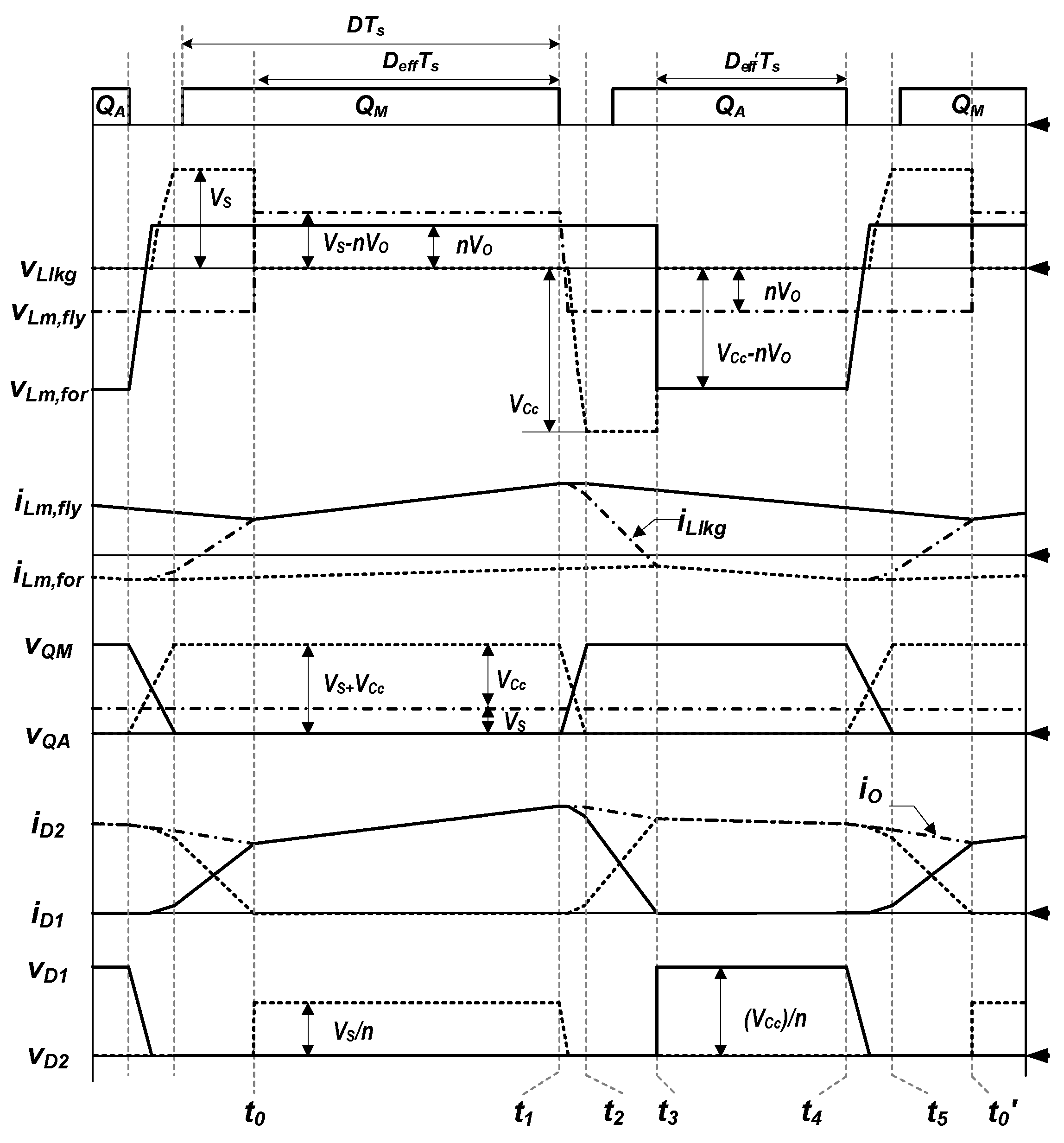
Figure 5 describes the key waveforms of the proposed converter. The operation of the proposed converter is equal to the conventional forward-flyback converter because the only difference between the conventional and the proposed converters is the integrated planar transformer. For the simplicity of the analysis, several assumptions are defined as follows:
(1)
All parasitic components are ignored except for parasitic components in Figure 4;
(2)
A clamp capacitor (CC) is large enough to be considered as a constant voltage source (VCc);
(3)
The output voltage (VO) is constant since the output is connected to the LV battery;
(4)
The transformer turns ratio (n) of the forward and flyback transformers (Tfor and Tfly) is N/1, where N is a number of the primary winding.
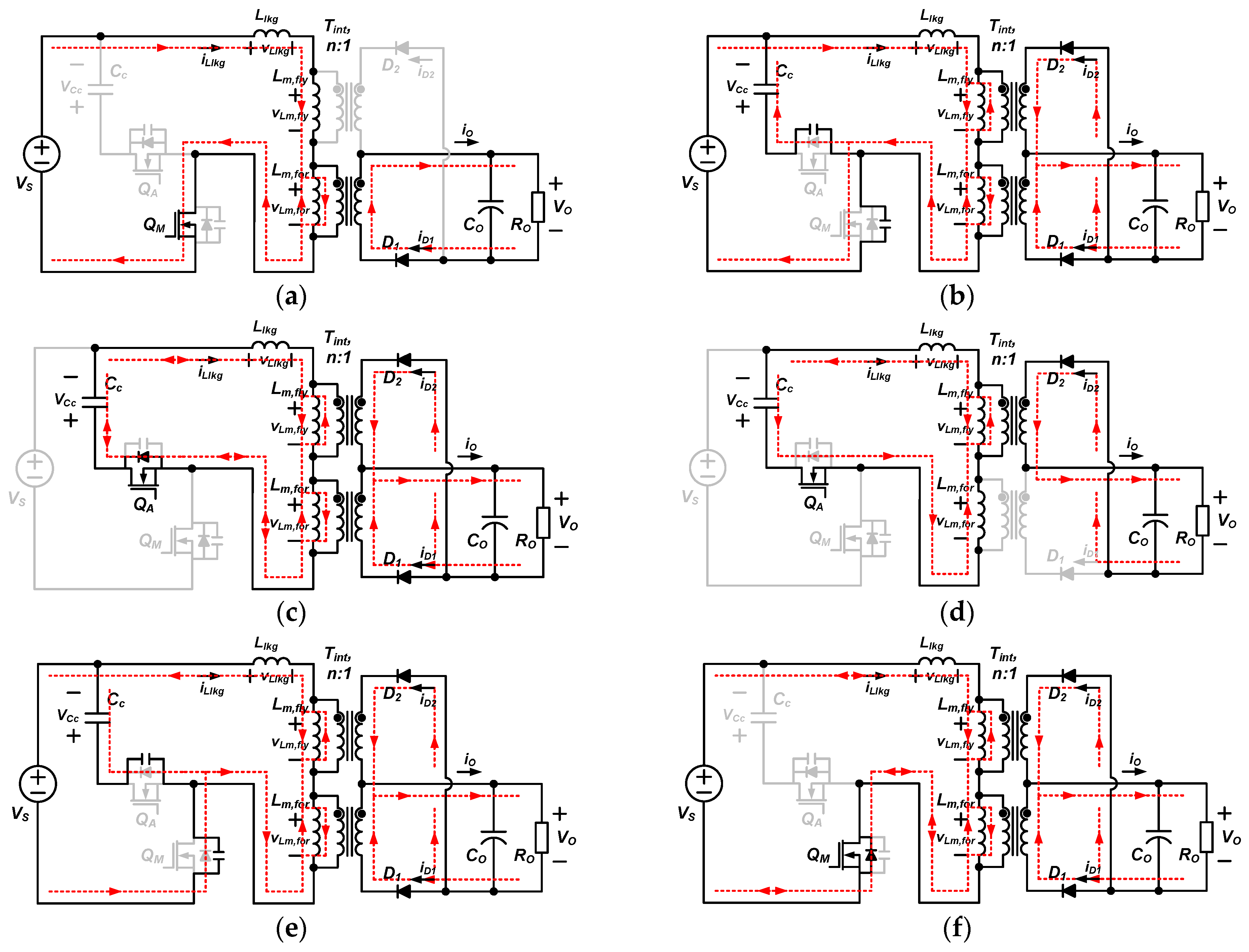
There are six operational modes for one switching period. Through the topological state shown in Figure 6, each operational mode can be explained as follows:
Mode 1 (t0t1): When the commutation of secondary diodes completes, and the leakage inductor current (iLlkg) becomes equal to the magnetizing current of Tfly (iLm,fly) at t0, mode 1 starts. During this mode, nVO is applied to the magnetizing inductance of Tfor (iLm,for). On the other hand, the applied voltage across the magnetizing inductance of Tfly (Lm,fly) is approximately VSnVO. The power is transferred from input to the output through QM and D1. During this period, iLm,for and iLm,fly linearly increase, and the diode1 (D1) current (iD1) can be represented as follows:
i L m , f o r ( t ) = i L m , f o r ( t 0 ) + n V O L m , f o r ( t t 0 ) ,
i L m , f l y ( t ) = i L l k g ( t ) = i L m , f l y ( t 0 ) + V S n V O L m , f l y ( t t 0 ) ,
i D 1 ( t ) = n ( i L m , f l y ( t ) i L m , f o r ( t ) ) .
Mode 2 (t1t2): After QM is turned off, mode 2 starts. During this mode, not only is output current reflected, but the stored energy in Llkg also charges an output capacitance of QM (COSSM) to VS + VCc and discharges an output capacitance of QA (COSSA) to 0 V. The voltage across Lm,fly reaches to −nVO, and the voltage on Llkg then starts to decrease to –VCc, inducing the commutation of secondary diodes.
Mode 3 (t2t3): After vQA decreases to zero, modes 3 begins. In this mode, iLlkg flows through the anti-parallel diode of QA, so it is possible to achieve the zero-voltage switching (ZVS) turn-on of QA. Since the sum of voltages across Lm,for and Lm,fly is zero, −VCc is applied to Llkg. As a result, iLlkg linearly decreases to iLm,for, as presented in (4), while the commutation of D1 and D2 simultaneously occurs.
i L l k g ( t ) = i L l k g ( t 2 ) V C c L l k g ( t t 2 ) .
Mode 4 (t3t4): After the completion of the commutation between D1 and D2, (VCc−nVO) is applied to Lm,for, and the reset of Tfor begins. At the same time, the voltage stress on D1 (vD1) increases to VCc/n. The energy stored in Lm,fly discharges, and it is transferred to the output through D2. Thus, the magnetizing and leakage currents of the transformers and D2 current are expressed as follows:
i L m , f o r ( t ) = i L l k g ( t ) = i L m , f o r ( t 3 ) V C c n V O L l k g ( t t 3 ) ,
i L m , f l y ( t ) = i L m , f l y ( t 3 ) n V O L m , f l y ( t t 3 ) ,
i D 2 ( t ) = n ( i L m , f l y ( t ) i L m , f o r ( t ) ) .
Mode 5 (t4t5): In this mode, QA is turned off, and the stored energies in Lm,for and Llkg charge and discharge COSSM and COSSA, respectively. As a result, vQA increases to VS + VCc while reducing vQM to zero. In addition, since vLm,for gradually increases to nVO, the sum of voltages across Lm,for and Lm,fly becomes zero, and the commutation of D1 and D2 starts.
Mode 6 (t5t0′): After vQM becomes zero, iLlkg flows through the anti-parallel diode of QM, so ZVS of QM can be achieved. Since the sum of voltages across Lm,for and Lm,fly is zero, VS is applied to Llkg. As a result, iLlkg linearly increases, as in (8), and finally matches iLm,fly as below:
i L l k g ( t ) = i L l k g ( t 5 ) + V S L l k g ( t t 5 ) .
During this period, the commutation of D1 and D2 simultaneously occurs, and after the commutation, Mode 1 begins again at t0.

3. Analysis of Proposed Converter

3.1. DC Conversion Ratio

The operation of the proposed converter with an integrated planar transformer is equal to a conventional active-clamp forward-flyback converter. Thus, considering the voltage-second balance of the flyback transformer and duty loss induced by the commutation of the secondary diode, the DC conversion ratio of the proposed converter can be derived as (9):
V O V S = 1 n ( D D L 1 ) L m , f o r L m , f o r + L l k g = 1 n ( D e f f ) L m , f o r L m , f o r + L l k g D n ,
where DL1 is Llkg·IO·fS/(n·VS), which represents duty loss resulting from the commutation period that occurs when QM is turned on, and Deff represents effective duty ratio. For concise analysis, provided that Llkg and DL1 are small enough to be ignored, the DC conversion ratio can be simplified as D/n.
From the voltage-second balance of the forward transformer, the clamp capacitor voltage and maximum voltage stress on the primary switches can be expressed as below:
V C c = D 1 D V S ,   V Q M = V Q A = 1 1 D V S .
Thus, as previously mentioned, the DC conversion of the proposed converter is equal to the conventional ACF and ACFF converters.

3.2. Design Consideration of Transformer

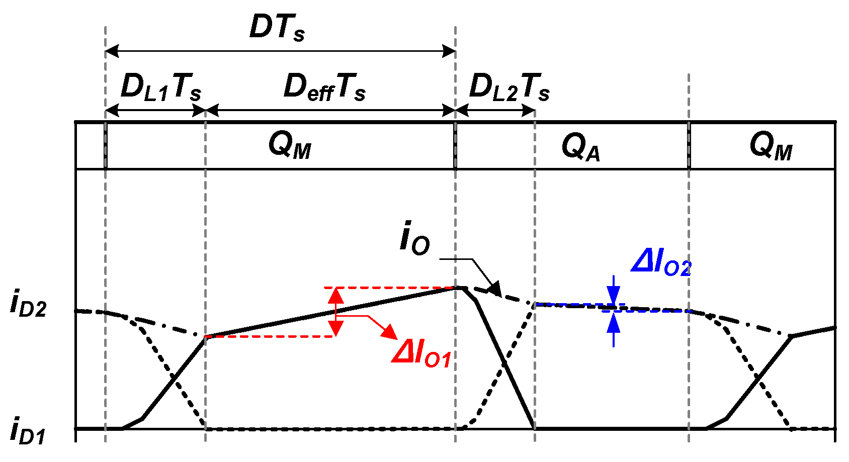
The conventional PSFB and ACF converters utilize two magnetic components, i.e., the transformer and the output inductor, and each magnetic component can be individually designed. For instance, the current ripple of the secondary side is solely determined by the inductance of the output inductor. On the other hand, the ACFF converter with an integrated planar transformer should be designed considering both Lm,for and Lm,fly to meet the current ripple and voltage ripple requirements. Based on the magnetizing inductances, output current variation according to switching states can be derived as below and shown in Figure 7:
Δ I O 1 = | ( k V S 2 n V O L m ) k n 2 V O T S V S | ,   Δ I O 2 = | ( 2 n V O k V C c L m ) k n 2 V O T S V C c | ,
where Δ I O 1 represents the output current variation when QM is turned on, Δ I O 2 is also the current ripple when QA is turned on, and k is Lm,for/(Lm,for + Llkg). Provided that the cores of the transformer are symmetric, Lm is the same as Lm,for and Lm,fly. From (11) and the current ripple conditions, the magnetizing inductance of the integrated planar transformer can be obtained.
The integrated planar transformer, as shown in Figure 4d and Figure 8, utilizes two separate UI cores. These two UI cores share the primary winding, and this primary winding is wound inside the cores to induce low EMI noise. One of UI cores operates like a forward transformer, which is a common transformer, and the other UI core acts as a flyback transformer, which is similar to an output inductor. Since the two UI cores are connected in a series, voltages applied to each magnetizing inductance of the transformers are distributed, enabling a low turn number of the primary side winding. Because of this, the number of primary windings of the integrated transformer is almost half that of conventional PSFB and ACF converters, and with this feature, a relatively low conduction loss can be achieved, making the integrated transformer suitable for a planar transformer. In addition, due to the simple secondary winding structure that passes through each UI core, it is easy to configure secondary windings in parallel, resulting in a reduced current density. Figure 8 shows the layout of the integrated planar transformer, and this integrated planar transformer is constructed with a four-layer PCB that is used for the power stage of the converter. The top and bottom layers consist of secondary windings in parallel, and the primary windings are wound through the second and third layer. In order to design and implement the integrated transformer, the maximum flux density (Bmax) and flux density variation (ΔB) of each core should be analyzed, and those can be derived as below:
Δ B f o r = ( D + D L 2 ) n V O T S N P A e , f o r ,   B f o r , max Δ B f o r 2 ,
Δ B f l y = ( 1 D + D L 1 ) n V O T S N P A e , f l y ,   B f l y , max L m , f l y I O n N P A e , f l y + Δ B f l y 2 ,
where DL2 is Llkg·IO·fS/(n·VCc), which represents the commutation period after QA is turned on. Based on (12) and (13), the core loss of the integrated transformer can be estimated by utilizing the improved generalized Steinmetz equation (IGSE) as shown in (14):
P c o r e = 1 T 0 T k i | d B d t | α ( Δ B ) β α d t ,   k i = k ( 2 π ) α 1 0 2 π | cos θ | α 2 β α d θ ,
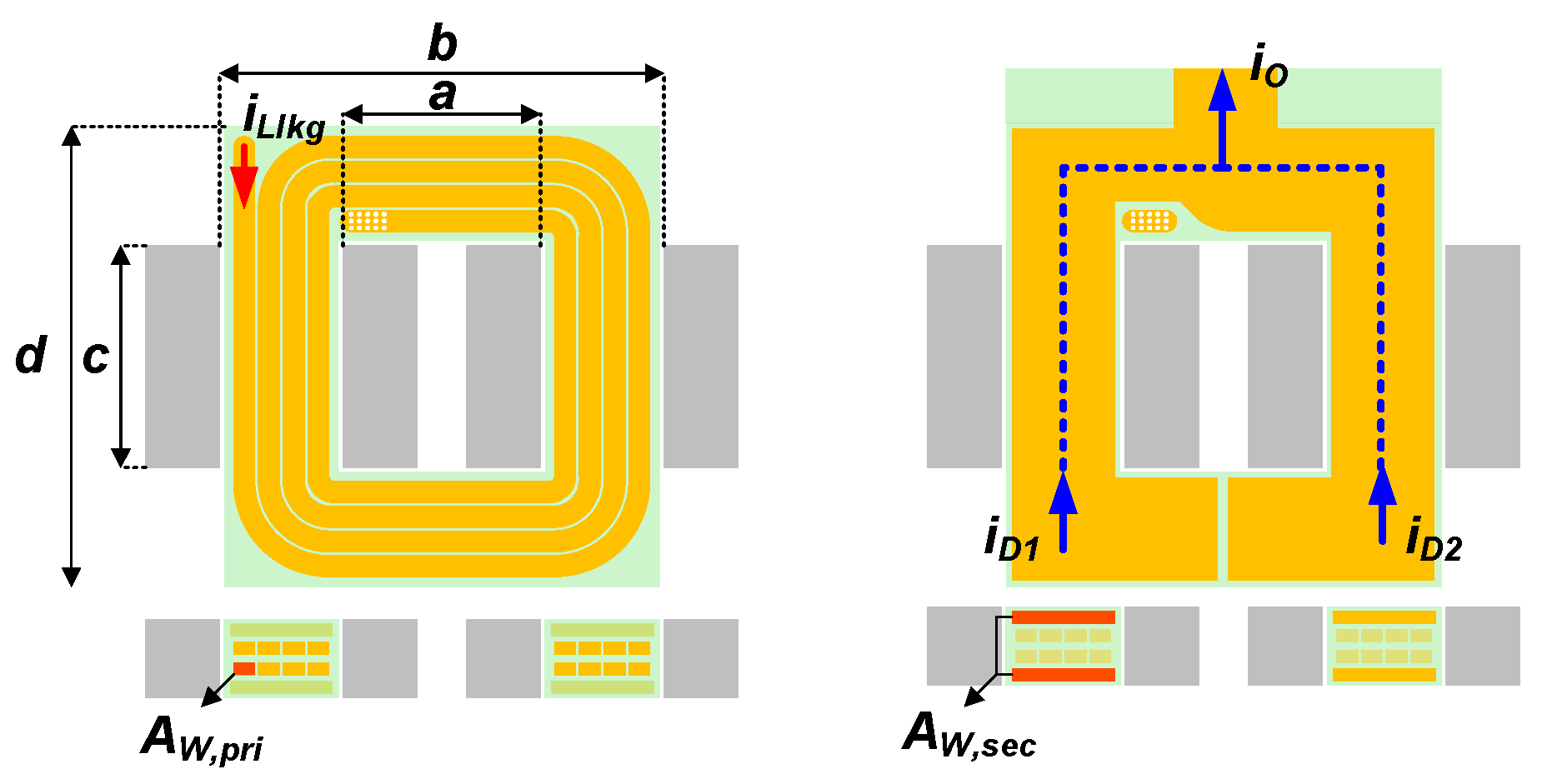
where k, α, and β are the same parameters as in the conventional Steinmetz equation [24]. The core loss of the planar integrated transformer is similar to the conventional integrated transformer with litz wire [20]. Meanwhile, the conduction loss of the planar transformer is considerably different from the conventional transformers because of the high wire resistance and high current density of the PCB windings. Based on Figure 9, the resistance of the primary and secondary windings can be derived as below:
R W , p r i = ρ c o p p e r { 1 + 0.00393 ( T c o p p e r 20 ) } M L T N p A W , p r i ,
R W , sec = ρ c o p p e r { 1 + 0.00393 ( T c o p p e r 20 ) } M L T 2 A W , sec ,
where MLT is the mean length turn, which can be represented as MLT = a + b + c + d. ρcopper is the conductivity of copper, and Tcopper is the temperature of copper. As previously mentioned, due to the reduced turn number of the primary windings, the PCB winding for the integrated planar transformer can be constructed through the second and third layers. In addition, because of the simple structure of the secondary winding, the secondary winding can be designed in parallel by assigning the top and bottom layers. As a result, the PCB windings can reduce the current density and the burden of the secondary wire. Despite the relatively high conduction loss of the planar transformer, the proposed integrated planar transformer provides a better structure without a high-cost metal PCB and increasing PCB layers compared with other planar transformers [21,22,23].
Table 1 shows the design results and loss analysis of the integrated planar transformer. The magnetizing and leakage inductances that are represented in Table 1 were acquired through Finite Element Method (FEM) analysis simulation, and core and conduction losses were derived based on (13)–(16). For the analysis, this converter and transformer were designed for 270 V input and 13.9 V/1.8 kW output specifications. As shown in Table 1, the total equivalent leakage inductance of the planar transformer is approximately 2 μH due to the highly coupled PCB windings, and it is relatively smaller than that of the conventional integrated transformer with litz wire and a busbar [20]. As a result, the integrated planar transformer can be designed with a high switching frequency, which results in a reduced volume of the transformer since the low leakage inductance leads to a small commutation period. Contrary to the volume of the transformer, the current density of the planar transformer, which is closely related to conduction loss, is much higher than that of the conventional transformer. Thus, almost five or six times more conduction loss of the planar transformer occurs. Despite the large conduction loss, the integrated planar transformer shows a significantly high power density and cost reduction; these characteristics have great strengths in mass production and make them very attractive to industrial providers. In order to support the consistency of the design results, additional FEM simulation was also conducted, and the simulation specifications and results are represented in Figure 10.
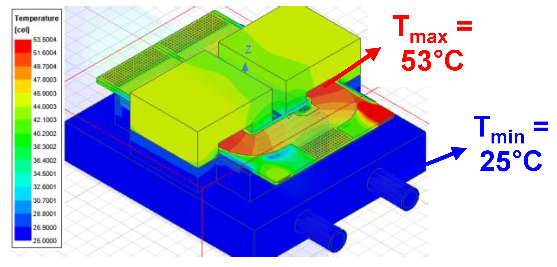
The high conduction loss of the PCB winding increases the PCB temperature, which can lead to the failure of the system. In order to prevent excessive temperature rise on the PCB, the PCB windings must be in direct contact with the heat sink to dissipate heat. Figure 11 illustrates the heat sink design for the PCB winding and presents the simulation result at full load conditions while water cooling at 9 ℓ/min and 25 °C ambient temperature are applied. As shown in Figure 11, although the planar transformer causes approximately 30 W power dissipation, the temperature rise is only below 30 °C. As a result, it can be seen that the PCB winding and integrated planar transformer are stable irrespective of the large conduction loss.
Generally, it is difficult to design planar magnetics when the magnetics require a high number of turns or turns ratio to prevent the flux saturation of the core. Meanwhile, the integrated planar transformer, which consists of the forward-flyback transformer, utilizes a low number of primary turns and turns ratio. This is because the series-connected transformer and the shared primary winding reduce the applied voltage on forward-flyback transformers as much as one-half those of conventional converters. Moreover, the simple structure of the secondary winding, paralleling of secondary windings though the top and bottom layers, possibly reduces the current density. Thus, it is possible to design a planar transformer with only four-layer PCB, which results in the minimized volume and cost of the transformer.

3.3. Loss Analysis of Proposed Converter

The RMS currents and voltage stresses on switches and diodes can be easily derived, as in Table 2, through the following assumptions:
(1)
The magnetizing inductances of the transformer are large enough, so the magnetizing current ripples of the transformer are small enough to be ignorable.
(2)
The leakage inductance of the transformer is small enough to be negligible, and because of that, the commutation periods can be ignorable.
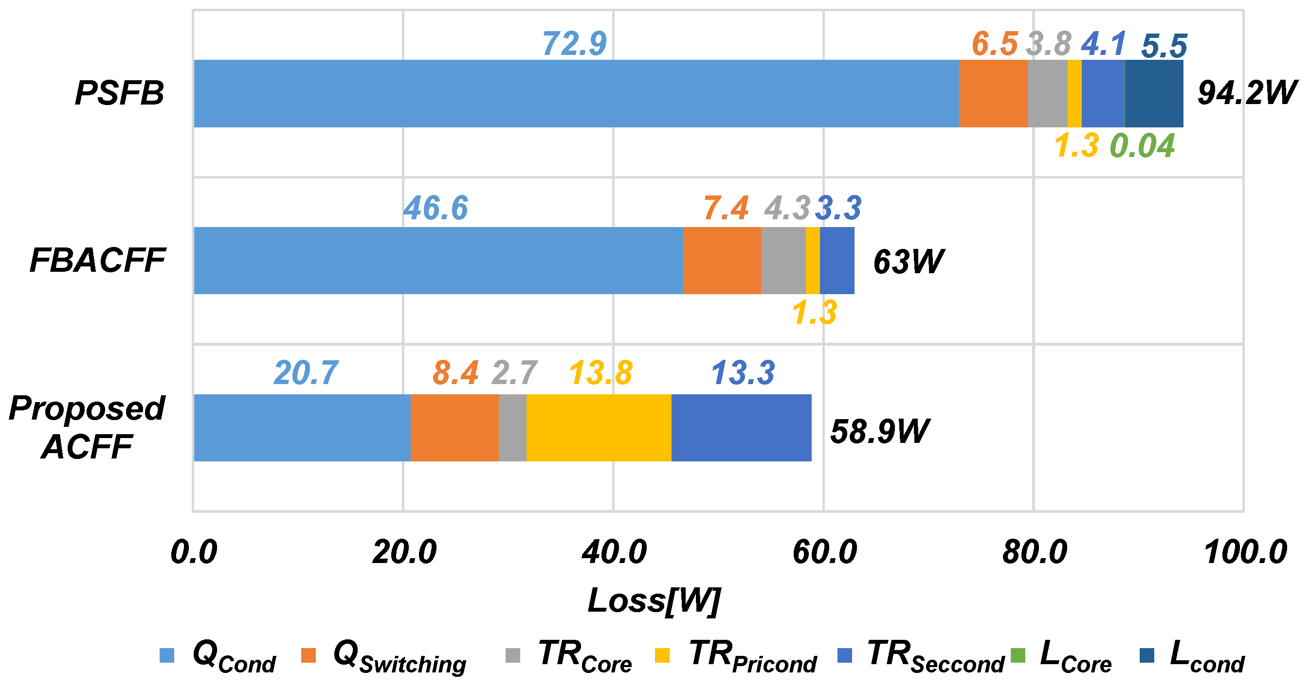
Because of the PCB winding of the integrated planar transformer, the conduction loss of the transformer is much higher than conventional converters. However, the proposed converter with an integrated planar transformer can achieve considerably low conduction loss on switches compared with the conventional PSFB and FBACFF converters because it derived from a conventional two-switch active-clamp structure. Figure 12 presents the loss analysis and comparison of the primary switches and the transformer, and for this analysis, IPW65R080CFDA and IPW65R190CFA were applied to the conventional FBACFF converter, C3M0120090D and C3M0280090D were used for the proposed converter, and the junction temperature was assumed to be 150 °C. As presented in Figure 12, the proposed converter with an integrated planar transformer can achieve similar or slightly higher efficiency compared with conventional converters even though it has a significantly improved power density. In addition, although the proposed LDC converter consists of the high-cost SiC MOSFET, due to the two switches and the planar transformer with four-layer PCB winding, the total cost of the converter is lower than that of other converters, and it is also highly cost competitive, as shown in Table 3. Furthermore, the proposed LDC converter can maximize the power density by eliminating the complex bobbin, reducing the height of the transformer, and obtaining the optimized structure of secondary rectifiers. Consequently, the proposed integrated planar transformer is suitable for mass production, and it is very attractive to manufacturers.

4. Experimental Results

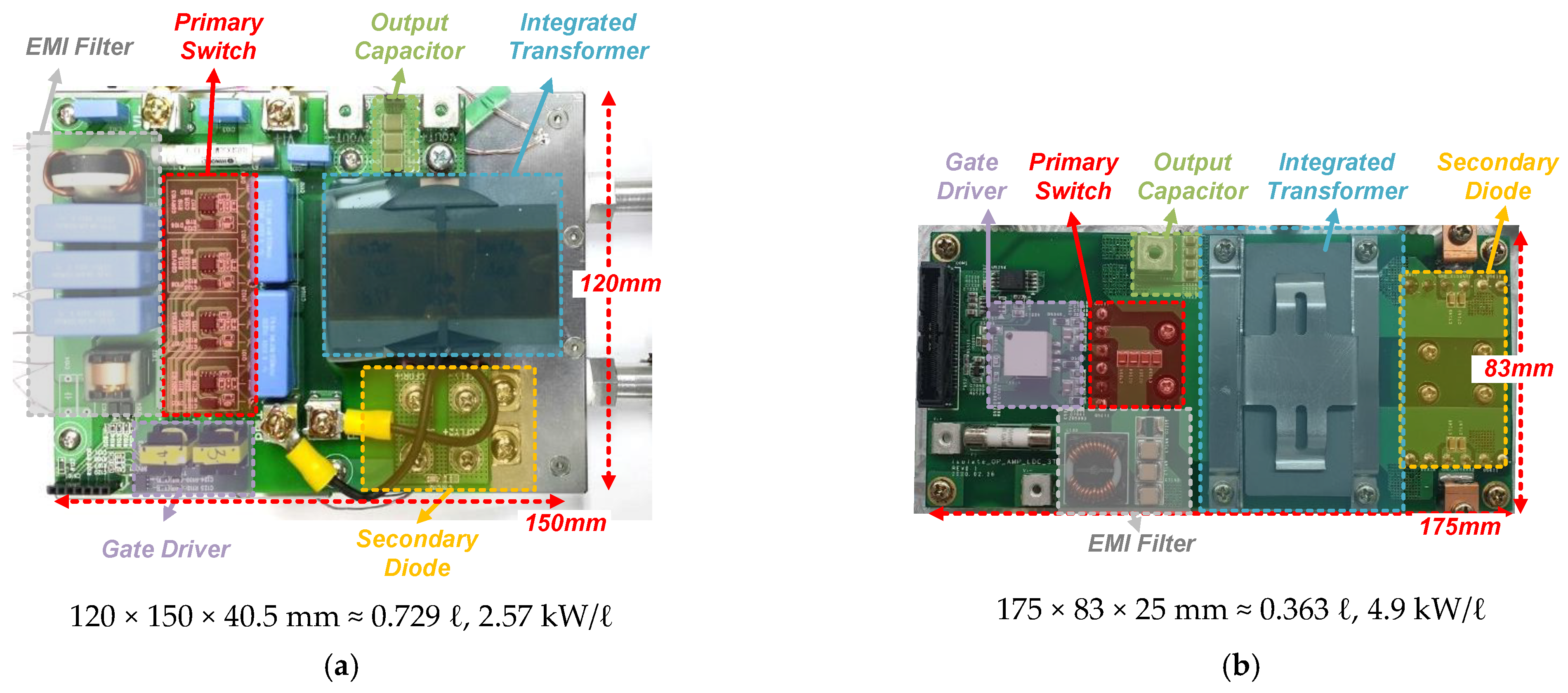
In order to support the effectiveness of the proposed converter with an integrated planar transformer, a prototype converter with the specifications of VS = 200–310 V, VO = 13.9 V, and fS = 200 kHz was designed and implemented. In addition, a conventional FBACFF converter was also constructed to compare efficiency and power density. As shown in Figure 13, the proposed converter showed considerably higher power density, i.e., 4.9 kW/ℓ, compared with that of the conventional converter, and this high power density is similar to the 700 kHz PSFB converter with a planar transformer presented in [22]. The detailed design parameters of the converters are represented and summarized in Table 4.
To confirm the consistency of design and provide high-accuracy measurements, an IDRC DSP1500WS series was used as the input source, and the output electronic load was a Chroma DC Electronic load 63203. In addition, the efficiency was measured by a YOKOGAWA WT5000 series, and a Lecroy Waverunner8000 was utilized to capture experimental waveforms.
Figure 14 shows the experimental waveforms at nominal input voltage conditions. As shown in Figure 14, the experimental waveforms of the proposed ACFF LDC converter were almost equal to the conventional ACF converter. The voltage stresses on the primary switches were up to 500 V, which was higher than the conventional FBACFF converter [20]. Although, the voltages stresses on switches were high, the proposed ACFF only adopts two switches and shows a reduced circulating current, inducing a relatively low conduction loss. Moreover, due to the significantly reduced conduction loss of the primary switches, it is able to achieve a high efficiency regardless of the increased conduction loss from the PCB windings of the planar transformer.
The other key experimental waveforms at the minimum and maximum input voltage and 100% load conditions are represented as shown in Figure 15 and Figure 16. At the minimum input voltage conditions, the high-voltage stresses on the primary switches, which were approximately 580 V, can be shown. This is because the large duty ratio for the output voltage regulation causes a high voltage on the clamp capacitor, which leads to high-voltage stresses on the primary switches. However, this high-voltage stress is far below the rating voltage of the SiC MOFSET, and the stability of the operation can be ensured. Because of the low leakage inductance of the integrated planar transformer, the small commutation period can be achieved, so it is possible to increase the switching frequency up to 200 kHz.
Figure 17 shows the soft-switching waveforms of the proposed converter. In 200 V input conditions, since the commutation period is relatively longer than that under other conditions, ZVS of QM can be achieved. Meanwhile, in high-input voltage conditions, as shown in Figure 17b, due to the small Llkg ≈ 2 µH and commutation periods, ZVS of QM cannot be accomplished. However, since VQM is reduced under 200 V at the instant of switch turn-on, the switching loss of QM is small enough to be ignorable. This is because the proposed converter not only adopts low-switching-loss SiC MOFSETs but also operates under 200 kHz switching frequency, unlike other over 500 kHz high-frequency converters utilizing a planar transformer, which are hugely affected by switching loss.
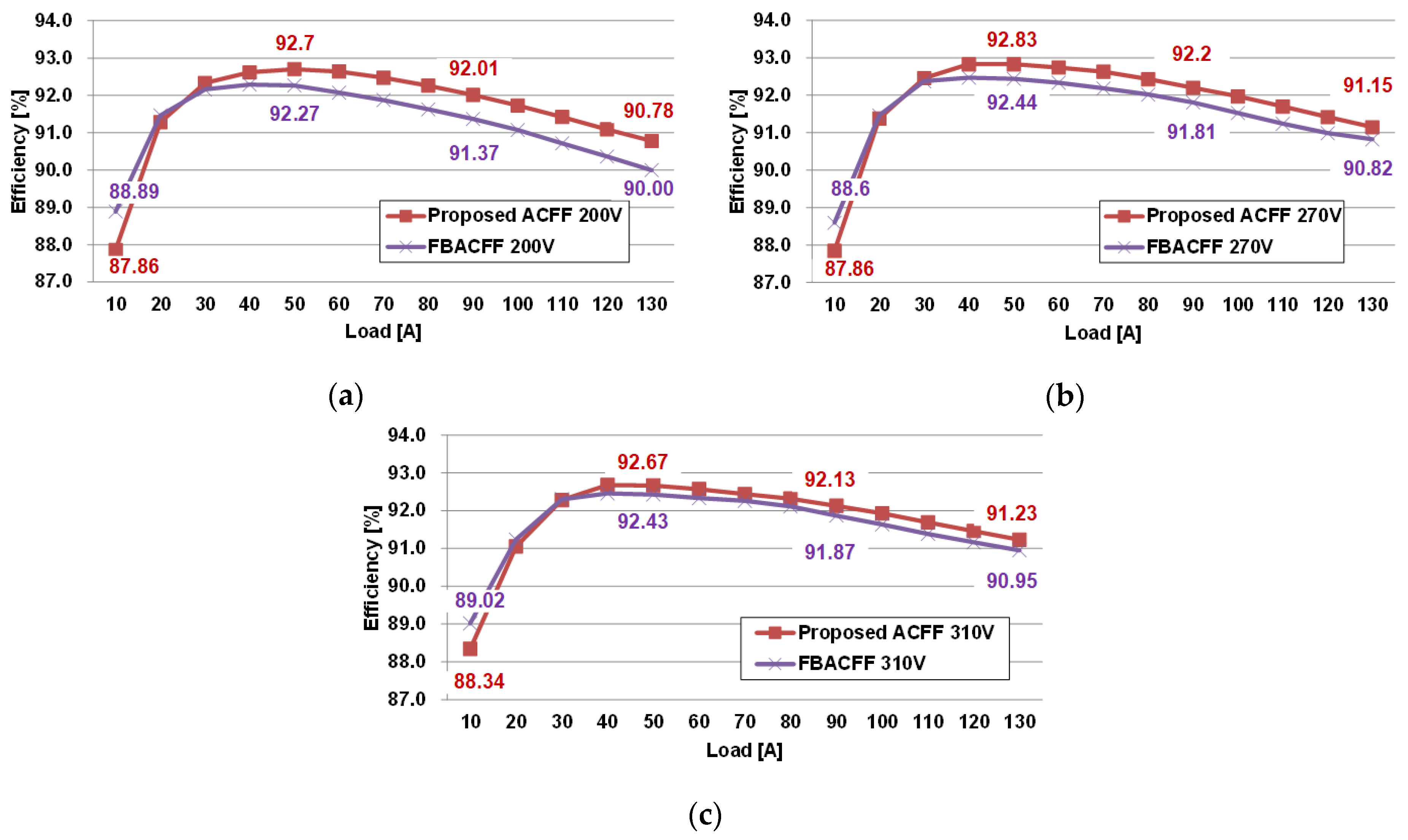
Figure 18 shows the measured efficiency of the proposed ACFF converter and the conventional FBACFF with an integrated transformer. As shown in these Figures, despite the large conduction loss of the integrated transformer, the proposed converter can achieve similar or slightly higher efficiency than the conventional converter. This is because the ACF converter has considerably low conduction loss resulting from the two-switch structure, which can make up for the large conduction loss of the integrated transformer. This is a very important characteristic of the proposed converter because conventional converters using planar magnetics suffer from degraded efficiency and narrow input and output voltage conditions. In addition, the proposed converter with an integrated planar transformer is very competitive in volume and cost. Consequently, the proposed converter adopting an integrated planar transformer is a very attractive solution, especially for LDC converters in automotive applications.

5. Conclusions

In this paper, a high-power-density active-clamp converter with an integrated planar transformer is presented. The integrated planar transformer for this converter makes it possible to achieve the maximized power density by magnetics integration, eliminating additional components for transformer winding, and simplifying the structure of the secondary rectifier. In addition, the proposed integrated planar transformer is considerably, highly cost-competitive because the PCB windings for the integrated planar transformer can be constructed through a 3oz and four-layer power stage PCB without any additional cost. Although there is still relatively high conduction loss of the transformer compared with that of a common copper wire transformer, the low primary conduction loss on the switches resulting from the active-clamp structure can compensate for the high conduction loss of the transformer, as well as lead to almost the same or a slightly higher efficiency than that of full-bridge converters. Furthermore, despite the high power density induced by a single transformer, the proposed converter can provide wide input and output voltage characteristics. Although it is difficult to increase the output power over 2 kW because of the relatively high current density of the PCB windings and high conduction loss of the proposed integrated transformer, under 2 kW output power, the proposed converter is a very promising converter due to the major features, such as its high power density, low cost, and wide voltage range. As a result, the proposed converter is not only suitable as an LDC converter in HEV and EV vehicles but is also a considerably attractive solution for various electric vehicle converter manufacturers, such as Vitesco, Hyundai, LG, and Denso.
In order to extend the applications and enhance the value of the proposed converter, research about increasing the output power up to 4 kW to supply stable power to an autonomous driving system should be conducted, and the bidirectional operation of the proposed converter should be researched for increasing its stability at the instant of ignition of the vehicle.

Author Contributions

Conceptualization, D.-W.L. and H.-S.Y.; methodology, D.-W.L.; validation J.-H.L. and D.-I.L.; formal analysis, D.-W.L.; writing—original draft preparation, D.-W.L. and H.-S.Y.; writing—review and editing, H.-S.Y.; visualization J.-H.L. and D.-I.L.; supervision, and project administration, and funding acquisition, H.-S.Y. All authors have read and agreed to the published version of the manuscript.

Funding

This research was funded by Incheon National University (International Cooperative) Research Grant in 2020. This work was supported by the National Research Foundation of Korea (NRF) grant funded by the Korea government (MSIT) (No. 2020R1C1C1010268).

Acknowledgments

This work was supported by Incheon National University (International Cooperative) Research Grant in 2020. This work was supported by the National Research Foundation of Korea (NRF) grant funded by the Korea government (MSIT) (No. 2020R1C1C1010268).

Conflicts of Interest

The authors declare no conflict of interest.

References

  1. Greenhouse Gas Emissions from a Typical Passenger Vehicle. Available online: https://www.epa.gov/greenvehicles/greenhouse-gas-emissions-typical-passenger-vehicle (accessed on 28 June 2022).
  2. Europe’s CO2 Emission Performance Standards for New Passenger Cars: Lessons from 2020 and Future Prospects. Available online: https://theicct.org/publication/europes-co2-emission-per-formance-standards-for-new-passenger-cars-lessons-from-2020-and-future-prospects (accessed on 28 June 2022).
  3. Global EV Outlook 2021. Available online: https://www.iea.org/reports/global-ev-outlook-2022 (accessed on 28 June 2022).
  4. Evolution of Vehicle Architecture. Available online: https://www.aptiv.com/newsroom/article/evolution-of-vehicle-architecture (accessed on 28 June 2022).
  5. Emadi, A.; Lee, Y.J.; Rajashekara, K. Power Electronics and Motor Drives in Electric, Hybrid Electric, and Plug-In Hybrid Electric Vehicles. IEEE Trans. Ind. Electron. 2008, 55, 2237–2245. [Google Scholar] [CrossRef]
  6. Noh, Y.S.; Hyon, B.J.; Park, J.S.; Kim, J.H.; Choi, J.H. Development of Low Voltage DC/DC Converter for Electric Vehicle using SiC MOSFET. In Proceedings of the 2019 International Symposium on Electrical and Electronics Engineering (ISEE), Ho Chi Minh City, Vietnam, 10–12 October 2019; pp. 237–240. [Google Scholar]
  7. Gu, B.; Lin, C.Y.; Chen, B.; Dominic, J.; Lai, J.S. Zero-Voltage-Switching PWM Resonant Full-Bridge Converter With Minimized Circulating Losses and Minimal Voltage Stresses of Bridge Rectifiers for Electric Vehicle Battery Chargers. IEEE Trans. Power Electron. 2013, 28, 4657–4667. [Google Scholar] [CrossRef]
  8. Kim, Y.D.; Lee, I.O.; Cho, I.H.; Moon, G.W. Hybrid Dual Full-Bridge DC–DC Converter With Reduced Circulating Current, Output Filter, and Conduction Loss of Rectifier Stage for RF Power Generator Application. IEEE Trans. Power Electron. 2014, 29, 1069–1081. [Google Scholar]
  9. Safaee, A.; Jain, P.; Bakhshai, A. A ZVS Pulsewidth Modulation Full-Bridge Converter with a Low-RMS-Current Resonant Auxiliary Circuit. IEEE Trans. Power Electron. 2016, 31, 4031–4047. [Google Scholar] [CrossRef]
  10. Zhao, L.; Li, H.; Wu, X.; Zhang, J. An Improved Phase-Shifted Full-Bridge Converter with Wide-Range ZVS and Reduced Filter Requirement. IEEE Trans. Ind. Electron. 2018, 65, 2167–2176. [Google Scholar] [CrossRef]
  11. Han, J.; Moon, G. High-Efficiency Phase-Shifted Full-Bridge Converter with a New Coupled Inductor Rectifier (CIR). IEEE Trans. Power Electron. 2019, 34, 8468–8480. [Google Scholar] [CrossRef]
  12. Park, K.; Kim, C.; Moon, G.; Youn, M. Three-Switch Active-Clamp Forward Converter with Low Switch Voltage Stress and Wide ZVS Range for High-Input-Voltage Applications. IEEE Trans. Power Electron. 2010, 25, 889–898. [Google Scholar] [CrossRef]
  13. Kim, C.; Baek, J.; Lee, J. Improved Three Switch-Active Clamp Forward Converter with Low Switching and Conduction Losses. IEEE Trans. Power Electron. 2019, 34, 5209–5216. [Google Scholar] [CrossRef]
  14. Li, W.; Li, P.; Yang, H.; He, X. Three-Level Forward–Flyback Phase-Shift ZVS Converter with Integrated Series-Connected Coupled Inductors. IEEE Trans. Power Electron. 2012, 27, 2846–2856. [Google Scholar] [CrossRef]
  15. Moon, S.; Park, K.; Moon, G.; Youn, M. Analysis and design of active clamp forward DC/DC converter with asymmetric two transformers. In Proceedings of the 8th International Conference on Power Electronics—ECCE Asia, Jeju, Korea, 30 May–3 June 2011; pp. 599–606. [Google Scholar]
  16. Lee, J.; Park, J.; Jeon, J.H. Series-Connected Forward–Flyback Converter for High Step-Up Power Conversion. IEEE Trans. Power Electron. 2011, 26, 3629–3641. [Google Scholar] [CrossRef]
  17. Lee, J.H.; Park, J.H.; Jeon, J.H. Series connected forward-flyback converter for high step-up power conversion. In Proceedings of the 8th International Conference on Power Electronics—ECCE Asia, Jeju, Korea, 30 May–3 June 2011; pp. 3037–3040. [Google Scholar]
  18. Chen, Q.; Feng, Y.; Zhou, L.; Wang, J.; Ruan, X. An improved Active Clamp Forward Converter with Integrated Magnetics. In Proceedings of the IEEE Power Electronics Specialists Conference, Orlando, FL, USA, 17–21 June 2007; pp. 377–382. [Google Scholar]
  19. Lin, J.Y.; Lo, Y.K.; Chiu, H.J.; Wang, C.F.; Lin, C.Y. An active-clamping ZVS flyback converter with integrated transformer. In Proceedings of the 2014 International Power Electronics Conference (IPEC-Hiroshima 2014—ECCE ASIA), Hiroshima, Japan, 18–21 May 2014; pp. 172–176. [Google Scholar]
  20. Baek, J.-I.; Youn, H.-S. Full-Bridge Active-Clamp Forward-Flyback Converter with an Integrated Transformer for High-Performance and Low Cost Low-Voltage DC Converter of Vehicle Applications. Energies 2020, 13, 863. [Google Scholar] [CrossRef] [Green Version]
  21. Planar Transformers for EV On-Board Chargers & DC-DC Converter Applications. Available online: https://standexelectronics.com/planar-magnetics/planar-transformers-for-ev-on-board-chargers-dc-dc-converter-applications/ (accessed on 14 July 2022).
  22. Naradhipa, A.M.; Kim, S.; Yang, D.; Choi, S.; Yeo, I.; Lee, Y. Power Density Optimization of 700 kHz GaN-Based Auxiliary Power Module for Electric Vehicles. IEEE Trans. Power Electron. 2022, 36, 5610–5621. [Google Scholar] [CrossRef]
  23. Kim, K.-W.; Jeong, Y.; Kim, J.-S.; Moon, G.-W. Low Common-Mode Noise LLC Resonant Converter With Static-Point-Connected Transformer. IEEE Trans. Power Electron. 2021, 36, 401–408. [Google Scholar] [CrossRef]
  24. Reinert, J.; Brockmeyer, A.; De Doncker, R.W. Calculation of losses in ferro- and ferrimagnetic materials based on the modified Steinmetz equation. IEEE Trans. Ind. Appl. 2001, 37, 1055–1061. [Google Scholar] [CrossRef]
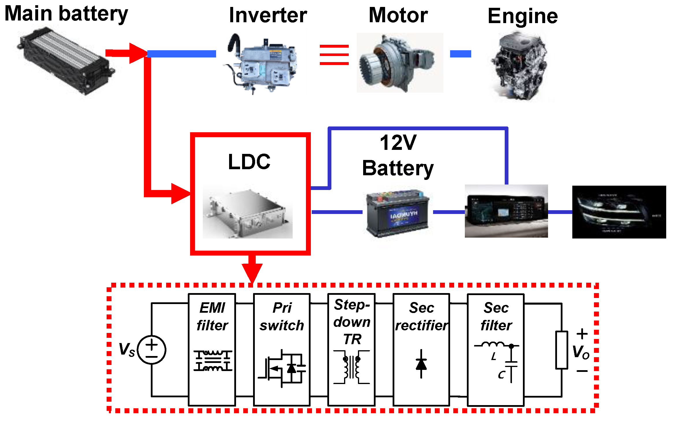
Figure 1. Low-voltage system of xEVs.
Energies 15 05609 g001
Figure 2. Conventional converters: (a) Phase-shifted full-bridge (PSFB) converter. (b) Active-clamp forward (ACF) converter. (c) Complex structure of transformer and secondary rectifier. (d) Conventional commercial planar transformer with about 2 kW output power.
Energies 15 05609 g002
Figure 3. Conventional converters with integrated transformer: (a) Integration of a transformer and an output inductor. (b) Integration of two transformers and windings wound outside the core. (c) Integration of two transformers sharing primary windings.
Energies 15 05609 g003
Figure 4. Proposed ACFF converter with integrated planar transformer: (a) Circuit diagram. (b) Circuit diagram with integrated transformer. (c) Structure of two conventional transformers with wire and busbar. (d) Structure of integrated planar transformer with PCB windings.
Energies 15 05609 g004
Figure 5. Key waveforms of ACFF LDC converter with integrated planar transformer.
Energies 15 05609 g005
Figure 6. Topological states of ACFF converter: (a) Mode1 (t0t1). (b) Mode2 (t1t2). (c) Mode3 (t2t3). (d) Mode4 (t3t4). (e) Mode5 (t4t5). (f) Mode6 (t5t0′).
Energies 15 05609 g006
Figure 7. Primary and secondary current waveforms of the proposed converter without dead-time.
Energies 15 05609 g007
Figure 8. Layout of integrated planar transformer: (a) Top layer. (b) Second layer. (c) Third layer. (d) Bottom layer.
Energies 15 05609 g008
Figure 9. Winding parameters of the integrated planar transformer.
Energies 15 05609 g009
Figure 10. Planar transformer core and conduction loss simulation at 270 V input and full load conditions.
Energies 15 05609 g010
Figure 11. Temperature rise according to the conduction loss of PCB winding at 270 V input and 100% load conditions.
Energies 15 05609 g011
Figure 12. Loss analysis of primary switches and magnetics at 270 V input and full load conditions.
Energies 15 05609 g012
Figure 13. Prototypes of conventional and proposed converters: (a) Conventional FBACFF converter with integrated transformer. (b) Proposed ACF converter with integrated planar transformer.
Energies 15 05609 g013
Figure 14. Key experimental waveforms at 270 V input and 100% load conditions: (a) Primary side key experimental waveforms. (b) Secondary side key experimental waveforms.
Energies 15 05609 g014
Figure 15. Key experimental waveforms at 200 V input and 100% load conditions: (a) Primary side key experimental waveforms. (b) Secondary side key experimental waveforms.
Energies 15 05609 g015
Figure 16. Key experimental waveforms at 310 V input and 100% load conditions: (a) Primary side key experimental waveforms. (b) Secondary side key experimental waveforms.
Energies 15 05609 g016
Figure 17. Soft-switching waveforms at full load conditions: (a) 200 V input. (b) 310 V input.
Energies 15 05609 g017
Figure 18. Measured efficiency according to input voltage: (a) Minimum input (VS = 200 V). (b) Nominal input (VS = 270 V). (c) Maximum input (VS = 310 V).
Energies 15 05609 g018
Table 1. Design results of the integrated planar transformer.
ParameterConventional Integrated TransformerProposed Integrated Planar
Transformer
V/VO, PO270 V/13.9 V, 1.8 kW
Switching frequency150 kHz200 kHz
CorePQ6640 customUI3323 × 2EA
Flux variation (ΔBfor/ΔBfly)0.16 T0.157 T/0.143 T
Core volume71,396 mm442,268 mm4
Primary windings area/current density (A/cm2)0.1Φ 250 strands/559 A/cm20.105 mm × 2.6 mm/4046 A/cm2
Resistance of primary winding0.014 Ω0.1 Ω
Secondary winding area/current density (A/cm2)2 mm × 10 mm/456 A/cm20.105 mm × 11.3 mm × 2/3737 A/cm2
Resistance of primary winding0.1 mΩ0.6 mΩ
Magnetizing inductance (Lm,for/Lm,fly)50 μH/40 μH30 μH/30 μH
Leakage inductance5 μH2 μH
Core loss4.28 W2.66 W
Primary winding loss1.34 W13.76 W
Secondary winding loss3.27 W13.33 W
Total loss of transformer8.89 W29.75 W
Table 2. Stress comparison of primary switches.
ParameterPSFBFBACFFProposed ACFF
RMS currents on switches (A) Q 1 Q 4 : I O n 2 Q 1 ,   Q 4 : I O n D , Q2, Q3 : – Q M :   I O n D , QA : –
Voltage stress on switches (V) Q 1 Q 4 : V S Q 1 ,   Q 2 :   V S ,   Q 3 ,   Q 4 :   D 1 D V S Q M :   1 1 D V S ,   Q A :   1 1 D V S
Voltage stresses on diodes (V) D 1 ,   D 2 : 2 V S n D 1 :   D n ( 1 D ) V S ,   D 2 : V S n D 1 :   D n ( 1 D ) V S ,   D 2 :   V S n
Table 3. Components and cost comparisons.
ParameterPSFBFBACFFProposed ACFF
Primary switch
Part number/Price ($)
Q1–Q4:
IPW65R115/4.636
Q1, Q4: IPW65R115/4.636,
Q2, Q3: IPW65R190/2.69
QM: C3M0120090/7.47
QA: C3M0280090/4.03
Total price of primary switches ($)18.54414.65211.5
Transformer/inductorEER4730
/EER6025
EE6630UI3323 × 2 EA
Price of magnetics($)20125
Total Price ($)38.54426.62516.5
Table 4. Parameters of Prototype Hardware.
ComponentsConventional FBACFF
with Integrated Transformer
Proposed ACF with Integrated
Planar Transformer
Primary switchQ1, Q4: IPW60R080
Q2, Q3: IPW60R190
QM: C3M0120090
QA: C3M0280090
Secondary diodeM80QZ12N, 2 EAVS-63CPQ100, 4 EA
Clamp capFilm: 630 V, 1 uFMLCC: 150 nF, 4 EA
TransformerCore: PQ6640,
Lm,for = 50 μH, Lm,fly = 40 μH
Llkg = 5 μH,
Np:Ns = 8:1
Core: UI3323, 2 EA,
Lm,for = Lm,fly = 30 μH,
Llkg = 2 μH,
Np:Ns = 8:1
Output capMLCC: 22 μF × 6 EAMLCC: 10 μF, 8 EA
Publisher’s Note: MDPI stays neutral with regard to jurisdictional claims in published maps and institutional affiliations.